News Posts matching #55nm

Return to Keyword Browsing

8-inch Wafer Capacity Remains Tight, Shortages Expected to Ease in 2H23, Says TrendForce

From 2020 to 2025, the compound annual growth rate (CAGR) of 12-inch equivalent wafer capacity at the world's top ten foundries will be approximately 10% with the majority of these companies focusing on 12-inch capacity expansion, which will see a CAGR of approximately 13.2%, according to TrendForce's research. In terms of 8-inch wafers, due to factors such as difficult to obtain equipment and whether capacity expansion is cost-effective, most fabs can only expand production slightly by means of capacity optimization, equating to a CAGR of only 3.3%. In terms of demand, the products primarily derived from 8-inch wafers, PMIC and Power Discrete, are driven by demand for electric vehicles, 5G smartphones, and servers. Stocking momentum has not fallen off, resulting in a serious shortage of 8-inch wafer production capacity that has festered since 2H19. Therefore, in order to mitigate competition for 8-inch capacity, a trend of shifting certain products to 12-inch production has gradually emerged. However, if shortages in overall 8-inch capacity is to be effectively alleviated, it is still necessary to wait for a large number of mainstream products to migrate to 12-inch production. The timeframe for this migration is estimated to be close to 2H23 into 2024.

GLOBALFOUNDRIES Offers Enhanced 55 nm CMOS Logic Process

GLOBALFOUNDRIES today announced additional enhancements to the foundry's 55-nanometer (nm) Low-Power Enhanced (LPe) process technology platform - 55nm LPe 1V - with qualified, next-generation memory and logic IP solutions from ARM. The 55nm LPe 1V is the industry's first and only enhanced process node to support ARM's 1.0/1.2V physical IP library, enabling chip designers to use a single process that supports two operating voltages in a single SoC.

"The key advantage of this 55nm LPe 1V offering is that the same design libraries can be used whether you are designing at 1.0 voltage or 1.2 voltage power option," said Bruce Kleinman, Vice President of Product Marketing at GLOBALFOUNDRIES. "What it means is that same set of design rules and models can be adopted, with no extra mask layer or special process required. This translates into cost saving and design flexibility without compromising on the power and optimization features."

SPARKLE Introduces Calibre X250/X250G Graphics Card with Abundant OC Capability

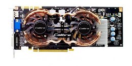
SPARKLE Computer Co., Ltd., the professional VGA card manufacturer and supplier, today announced the Calibre X250 512MB/X250G 1GB GDDR3 Graphics Card with Calibre Dual Fly Fan and SPA Tune OC software, extending the DirectX 10 gaming performance of GeForce GTS 250 GPU to a new level, bringing vivid DX10 gaming graphics on a mainstream consumer computing platform.

Calibre X250/X250G Graphics Card features a 55nm chip process from TSMC. So It has groundbreaking speeds compared with ordinary GeForce GTS 250 graphics cards on market, the core speed is raised from 738MHz to 761MHz, the shader clock is raised from 1836MHz to 1911MHz, making it can deliver unrivaled graphics performance in the hottest games including Far Cry 2, Mirror's Edge, and Call of Duty 5: World at War. The Calibre X250/X250G Graphics Card adopts Calibre non-reference PCB design, providing enhanced power circuitry with more phases of vGPU power circuit and vMem circuit. Also it only uses solid capacitors with lower power loss, providing more stable and longer product lifespan.

Zotac Readying Custom-Design GTX 285 Accelerator

NVIDIA seems to have lifted restrictions over manufacturers coming up with their own designs for the GeForce GTX 285 accelerator, barely a month into its market introduction. Zotac, backed by the engineering prowess of PCPartner seems to have already designed their custom-PCB according to a finding by Expreview. The new PCB employs a decent bit of component rearrangement.

Perhaps the most significant part of that rearrangement comes from moving the vMem circuit that powers the card's 16 memory chips to its anterior end, in between the NVIO2 processor and the SLI connectors. The PCB uses a new MOSFET arrangement that groups them in a DPAK group. The vGPU circuit consists of 6 phases, and the vMem circuit 2. Zotac makes use of an aluminum support-brace around the G200b graphics processor, which serves as a safety measure for the GPU, minimizing the impact of PCB bending on the fragile ball-grid, especially with 55nm GeForce GTX 260 and GTX 285 lacking a back-plate that counters PCB bending. The orange-coloured DVI connectors make it distinctively Zotac. The SKU based on the new PCB may feature reference clock speeds of 648/2484/1476 MHz (core/memory/shader). Its cooler design remains unknown.

Inno3D GeForce GTX 260 P897 PCB Pictured

NVIDIA has come up with a new inexpensive reference PCB design for the GeForce GTX 260 (55nm) codenamed P897. The new PCB does away with the numerous redundant and rudimentary connections, excessive PCB layers and some components. The new PCB design is expected to reduce manufacturing costs by as much as $15.

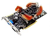
Inno3D will be one of the first companies to come up with a model based on the new PCB. The company is planning an accelerator using the P897 PCB and a cooler of its own. Expreview sourced a few pictures of the card. While the cooler itself isn't pictured, we can make a safe guess that it is going to be something along the lines of its previous Freezer Direct Heatpipe-Touch (DHT) series models, in which the heatpipes of the cooler make direct contact with the GPU to convey heat. Inno3D is expected to start mass-production of this accelerator soon, following which it will assign an SKU and price it. While the new PCB cuts manufacturing costs, it remains to be seen as to what extant NVIDIA's partners pass on the benefit to the consumer.

Palit Launches GeForce GTX 260 SONIC 216SP

Palit Microsystems, leading graphics card manufacturer, introduces the 55nm graphics processor: Palit GeForce GTX260 Sonic 216SP. The overclocked edition Palit GTX260 Sonic 216SP is the first custom designed graphics card that combines the innovative DUAL FAN cooling system with the high performance ad power efficiency of 55nm GPU to deliver the perfect solution for the gaming enthusiast.

Leadtek Launches New WinFast GTX260 55nm EXTREME+

LEADTEK Research Inc., world acclaimed for its extremevisual graphics leading brand technology, proudly announces its latest WinFast GTX 260 EXTREME+ with a new graphics card packaging design. Based on the Best-in-class NVIDIA GTX 260 chipsets, this thoroughbred graphics card delivers advanced performance with the best cooling silent fansink. Its overclocking capability is sure to bring users a fantasy visual effect. Together with the launch of the graphics card, Leadtek debuts a new packaging design. The latter replaces the former robots with a series of top speed cars as the key visual. This original concept aims to vaunt Leadtek's corporate spirit of "high quality & speedy performance" that gives users an altogether new visual impression.

WinFast GTX 260 EXTREME+ is powered up with 2nd Generation NVIDIA Unified Architecture and enables the rendering of multiple, true-to-life characters in complex and dynamic virtual worlds. In addition, the latest parallel computing architecture with massive independent processing cores enables GTX 260 EXTREME+ to execute the most intricate non-gaming applications via CUDA language. This includes acceleration of the art design application - science simulation application or transcoding of video to a personal video player up to 7X faster than the CPU.

NVIDIA GeForce GTX 285 and GeForce GTX 295 Launch Dates Announced

It's time for some new information, provided by our colleagues over at OCWorkBench. As reported by them NVIDIA is preparing to launch its new GeForce GTX 285 card on January 15th, while the dual-GPU GeForce GTX 295 is planned to debute on January 8th, during the first day of CES 2009. These two video cards will be NVIDIA's future top performing products. We're already familiar with the specs of GeForce GTX 285. It will be based on a 55nm production node with 183W TDP, and will have reference clock speeds of 648MHz for the core, 1476MHz for the shaders, and 1100MHz (x2) for the memory. On the other side, NVIDIA GeForce GTX 295 is a dual PCB, dual GPU card, that will beat the mighty ATI Radeon 4870 X2. Some of the facts that we already know include: 2x GPUs with a total of 480 shader processors, 1792MB memory (896MB per GPU), 576MHz core frequency, 1242MHz shader frequency, 999MHz DDR3 memory frequency, and Quad-SLI support. That's all folks, put aside some $ for next week.

GeForce GTX 285 from Gigabyte Appears in Hong Kong

Though no official information from NVIDIA has been released on the GeForce GTX 285, through leaks over the past month we know that this is a 55nm version of the GTX280. Although the 55nm GTX 260 has kept its name, it seems that the same cannot be said of the GTX 280. This Gigabyte card is said to use the same reference clock speeds as seen in the review from Computerbase.de which we covered just a few days ago. With a product code of GV-N285-1GH-B, it has 1GB of GDDR3 at 2484 MHz, 240SP's at 1476 MHz and a core at 648 MHz. According to TechConnect the Gigabyte GeForce GTX 285 has been found with prices as low as $412.8 (€296.3).

EVGA Makes its 55nm GeForce GTX 260 Lineup Official, Intros SSC Variant

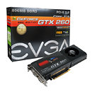
About a week into its market introduction, EVGA today made its 55nm GeForce GTX 260 graphics cards lineup official. The company also introduced a premium Super-Superclocked (SSC) variant of the said card. While having identical reference clock speeds to those of the 65nm GeForce GTX 260 Core-216 lineup, the new lineup offers higher energy efficiency and improved thermal characteristics.

The SSC variant introduced has clock speeds of 675 MHz (core), 1,458 MHz (shader) and 2,304 MHz (memory). It is backed by the EVGA limited lifetime warranty. EVGA also disclosed the suggested retail prices for the entire lineup (North American region) in its press-release, so you know which prices to buy them at: US $259.99 for the base model (896-P3-1255-AR), $269.99 for the Superclocked model (896-P3-1257-AR) and $289.99 for the SSC model (896-P3-1258-AR).

G92-Based GeForce 9 Series Products to be Renamed GeForce GTS 200 Series

The NVIDIA G92 graphics processor has had the reputation of spanning across two generations of GeForce graphics accelerators, which could well become three with talk about NVIDIA executing another re-branding to products based on the GPU. The re-branding will use the B1 revision of the G92 GPU (aka G92b), which is known to have been manufactured on the 55nm fabrication process, along with the 65nm A1 revision.

The new series created will include two SKUs based on the G92, the GeForce GTS 240 and GeForce GTS 250. These are the 112 SP and 128 SP variants of the G92 core, presently branded under 8800/9800 GT and 8800 GTS 512, 9800 GTX/GTX+ respectively. NVIDIA looks to capitalise on the sales improvement the GTX 200 series has seen for the past two or so months now, by giving it a present-generation branding. The re-branding, or rather, releasing products with the new naming scheme is said to be operationalised by February 2009.

RV740 Successfully Taped Out, Other 40nm GPUs Follow

The RV740 graphics processor by AMD could well be the first GPU in production, to be built on the newer 40nm manufacturing process, giving its makers something to brag about. The RV740 design and specifications are largely derived from the RV770LE (covered here), while bringing the GDDR5 memory standard to the mainstream.

Chinese industrial journals tell DigiTimes that the company has completed taping-out the RV740, and that the GPU is awaiting mass-production by AMD's foundry partner, Taiwan Semiconductor Manufacturing Company (TSMC). Mass production of products based on this GPU could commence by the end of Q1 2009.

EVGA 55nm GeForce GTX 260 Ready for Launch

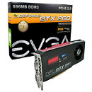
With NVIDIA being ready with variants of the G200 graphics processors based on the 55nm manufacturing process, a fleet of new graphics cards are in the line for launches. The range starts with a sub-$300 offering, the GeForce GTX 260 55nm. You now have three SKUs that share the name "GeForce GTX 260". The GeForce GTX 260 comes with the 216 SP configuration with 896 MB of GDDR3 memory. EVGA for one, is aiming to be one of the first NVIDIA partners to be out with the new GeForce GTX 260, with a standard and Superclocked models ready for launch, already listed in European and North American online stores.

The EVGA 896-P3-1255-AR comes with NVIDIA reference clock speeds of 576 MHz (core), 1242 MHz (shader) and 999 MHz (memory), while the Superclocked EVGA 896-P3-1257-AR model is factory-overclocked with 626 MHz (core), 1350 MHz (shader) and 1053 MHz (memory). EVGA is further planning a SSC variant that could come with a core clock speed of 666 MHz. For now, American retailer ZipZoomFly has listed the reference speed card for $289.99 and the Superclocked variant for just $4 more. Both cards are listed as "pre-order".

55nm GeForce GTX260 by Inno3D Found on Sale in Japan

It seems that the first graphics card using NVIDIA's latest 55nm fabrication process has in fact reached retail earlier than the January 2009 release date we had previously anticipated. A Japanese technology website has photos of an Inno3D GeForce GTX260 Gold featuring a factory overclocked, 216 SP chip, made by the 55nm process. What is interesting is that Inno3D have clearly advertised this fact by displaying 55nm on the product and in the product description. The core clock is set at 620Mhz with a memory clock of 1050Mhz, there is no information as yet on the shader clock. It can also be seen that there are no memory chips on the rear of the PCB, this means that all the memory chips are cooled by the stock cooler and there is no longer a need for backplates, as seen on many 65nm GT200 based cards. The pricing however does seem a little steep, with today's exchange rate, this would set you back around $390 USD, with online stores selling the 65nm equivalent for over $100 less, one would hope that the price will drop before it reaches the rest of the world's shores.
Return to Keyword Browsing
Jan 22nd, 2025 14:57 EST change timezone

New Forum Posts

Popular Reviews

Controversial News Posts