Apr 16th, 2025 08:52 EDT
change timezone
Latest GPU Drivers
New Forum Posts
- Last game you purchased? (771)
- GPU Memory Temprature is always high (16)
- Windows 11 fresh install to do list (20)
- 5070ti overclock...what are your settings? (3)
- Help For XFX RX 590 GME Chinese - Vbios (4)
- PCGH: "hidden site" to see total money spend on steam (3)
- Share your AIDA 64 cache and memory benchmark here (3053)
- NVFlash for RTX 50 Series (Blackwell) (0)
- intel 1700 with high speed ram,memory (63)
- The TPU UK Clubhouse (26115)
Popular Reviews
- G.SKILL Trident Z5 NEO RGB DDR5-6000 32 GB CL26 Review - AMD EXPO
- ASUS GeForce RTX 5080 TUF OC Review
- DAREU A950 Wing Review
- The Last Of Us Part 2 Performance Benchmark Review - 30 GPUs Compared
- Sapphire Radeon RX 9070 XT Pulse Review
- Sapphire Radeon RX 9070 XT Nitro+ Review - Beating NVIDIA
- Upcoming Hardware Launches 2025 (Updated Apr 2025)
- Thermaltake TR100 Review
- Zotac GeForce RTX 5070 Ti Amp Extreme Review
- TerraMaster F8 SSD Plus Review - Compact and quiet
Controversial News Posts
- NVIDIA GeForce RTX 5060 Ti 16 GB SKU Likely Launching at $499, According to Supply Chain Leak (182)
- NVIDIA Sends MSRP Numbers to Partners: GeForce RTX 5060 Ti 8 GB at $379, RTX 5060 Ti 16 GB at $429 (124)
- Nintendo Confirms That Switch 2 Joy-Cons Will Not Utilize Hall Effect Stick Technology (105)
- Over 200,000 Sold Radeon RX 9070 and RX 9070 XT GPUs? AMD Says No Number was Given (100)
- Nintendo Switch 2 Launches June 5 at $449.99 with New Hardware and Games (99)
- Sony Increases the PS5 Pricing in EMEA and ANZ by Around 25 Percent (85)
- NVIDIA PhysX and Flow Made Fully Open-Source (77)
- NVIDIA Pushes GeForce RTX 5060 Ti Launch to Mid-April, RTX 5060 to May (77)
News Posts matching #6nm
Return to Keyword Browsing
Phison Shows Off 6nm E28 NVMe Gen 5 Controller; E31T with Micron G9, and a Massive Enterprise SSD
At CES 2025, we found the SSD controller that will spur high-end NVMe Gen 5 SSD adoption. Until now, high-end Gen 5 SSDs were driven by Phison's E26 series controller that the company built on TSMC's 12 nm process. The company on Monday launched the new E28 series controller (full name PS5028-E28). This chip is built on the much more advanced TSMC 6 nm process. The new process lets Phison to significantly lower the electrical cost of its NAND flash interface serializer-deserializer, and step up performance closer to the interface limits of PCI-Express 5.0 x4. The controller offers sequential speeds of up to 14.5 GB/s, which is an increase from last year's E26 Max14um variant.
The company showed us the bare E28 controller chip, and a reference-design SSD based on it. Not much to report, except that the drive lacked any cooling solution. Production SSDs powered by the E28 will still need heatsinks to achieve optimal performance, although they won't run as hot as drives powered by the E26. The company didn't have any performance demo stations set up with this drive.


The company showed us the bare E28 controller chip, and a reference-design SSD based on it. Not much to report, except that the drive lacked any cooling solution. Production SSDs powered by the E28 will still need heatsinks to achieve optimal performance, although they won't run as hot as drives powered by the E26. The company didn't have any performance demo stations set up with this drive.


Silicon Motion Unveils 6nm UFS 4.0 Controller for AI Smartphones, Edge Computing and Automotive Applications
Silicon Motion Technology Corporation ("Silicon Motion"), a global leader in designing and marketing NAND flash controllers for solid state storage devices, today introduced its UFS (Universal Flash Storage) 4.0 controller, the SM2756, as the flagship of the industry's broadest merchant portfolio of UFS controller solutions for the growing requirements of AI-powered smartphones as well as other high-performance applications including automotive and edge computing. The company also added a new, second generation SM2753 UFS 3.1 controller to broaden its portfolio of controllers now supporting UFS 4.0 to UFS 2.2 standards. Silicon Motion's UFS portfolio delivers high-performance and low power embedded storage for flagship to mainstream and value mobile and computing devices, supporting the broadest range of NAND flash, including next-generation high speed 3D TLC and QLC NAND.
The new SM2756 UFS 4.0 controller solution is the world's most advanced controller, built on leading 6 nm EUV technology and using MIPI M-PHY low-power architecture, providing the right balance of high performance and power efficiency to enable the all day computing needs of today's premium and AI mobile devices. The SM2756 achieves sequential read performance exceeding 4,300 MB/s and sequential write speeds of over 4,000 MB/s and supports the broadest range of 3D TLC and QLC NAND flash with densities of up to 2 TB.
The new SM2756 UFS 4.0 controller solution is the world's most advanced controller, built on leading 6 nm EUV technology and using MIPI M-PHY low-power architecture, providing the right balance of high performance and power efficiency to enable the all day computing needs of today's premium and AI mobile devices. The SM2756 achieves sequential read performance exceeding 4,300 MB/s and sequential write speeds of over 4,000 MB/s and supports the broadest range of 3D TLC and QLC NAND flash with densities of up to 2 TB.


AMD Makes Radeon Pro W7900 & W7800 Workstation GPUs Official
AMD unveils the most powerful AMD Radeon Pro graphics cards, Offering unique features and leadership performance to tackle heavy to Extreme Professional Workloads - AMD today announced the AMD Radeon PRO W7000 Series graphics, its most-powerful workstation graphics cards to date. The AMD Radeon PRO W7900 and AMD Radeon PRO W7800 graphics cards are built on groundbreaking AMD RDNA 3 architecture, delivering significantly higher performance than the previous generation and exceptional performance-per-dollar compared to the competitive offering. The new graphics cards are designed for professionals to create and work with high-polygon count models seamlessly, deliver incredible image fidelity and color accuracy, and run graphics and compute-based applications concurrently without disruption to workflows.
AMD Radeon PRO W7000 Series graphics cards feature the world's first workstation GPU architecture based on AMD's advanced chiplet design, providing real-world multi-tasking performance and incredible power efficiency. The new graphics cards are also the first professional workstation GPUs to offer the new AMD Radiance Display Engine featuring DisplayPort 2.1 that delivers a superior visual experience, higher resolutions and more available colors than ever before.


AMD Radeon PRO W7000 Series graphics cards feature the world's first workstation GPU architecture based on AMD's advanced chiplet design, providing real-world multi-tasking performance and incredible power efficiency. The new graphics cards are also the first professional workstation GPUs to offer the new AMD Radiance Display Engine featuring DisplayPort 2.1 that delivers a superior visual experience, higher resolutions and more available colors than ever before.


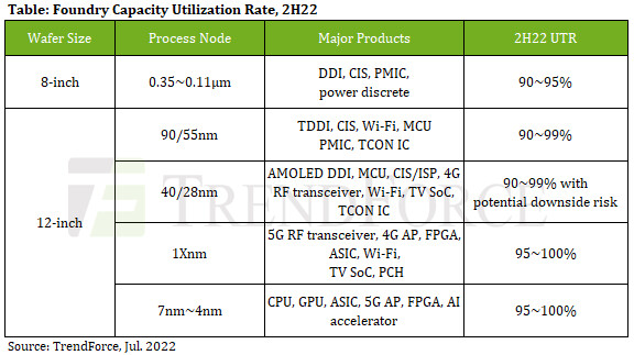
Semiconductor Fab Order Cancellations Expected to Result in Reduced Capacity Utilization Rate in 2H22
According to TrendForce investigations, foundries have seen a wave of order cancellations with the first of these revisions originating from large-size Driver IC and TDDI, which rely on mainstream 0.1X μm and 55 nm processes, respectively. Although products such as MCU and PMIC were previously in short supply, foundries' capacity utilization rate remained roughly at full capacity through their adjustment of product mix. However, a recent wave cancellations have emerged for PMIC, CIS, and certain MCU and SoC orders. Although still dominated by consumer applications, foundries are beginning to feel the strain of the copious order cancellations from customers and capacity utilization rate has officially declined.
Looking at trends in 2H22, TrendForce indicates, in addition to no relief from the sustained downgrade of driver IC demand, inventory adjustment has begun for smartphones, PCs, and TV-related peripheral components such as SoCs, CIS, and PMICs, and companies are beginning to curtail their wafer input plans with foundries. This phenomenon of order cancellations is occurring simultaneously in 8-inch and 12-inch fabs at nodes including 0.1X μm, 90/55 nm, and 40/28 nm. Not even the advanced 7/6 nm processes are immune.
Looking at trends in 2H22, TrendForce indicates, in addition to no relief from the sustained downgrade of driver IC demand, inventory adjustment has begun for smartphones, PCs, and TV-related peripheral components such as SoCs, CIS, and PMICs, and companies are beginning to curtail their wafer input plans with foundries. This phenomenon of order cancellations is occurring simultaneously in 8-inch and 12-inch fabs at nodes including 0.1X μm, 90/55 nm, and 40/28 nm. Not even the advanced 7/6 nm processes are immune.
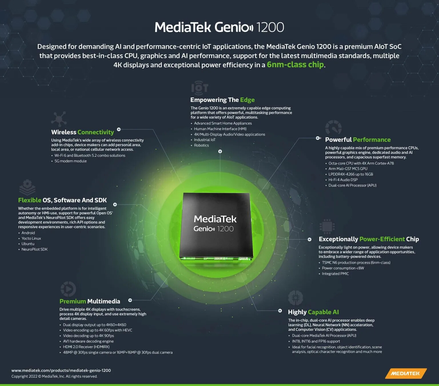
MediaTek Unveils New AIoT Platform Stack and Introduces the Genio 1200 AIoT Chip
MediaTek today unveiled its new Genio platform for AIoT devices and introduced the first chip in the Genio family, the Genio 1200 designed for premium AIoT products. MediaTek Genio is a complete platform stack for the AIoT with powerful and ultra- efficient chipsets, open platform software development kits (SDKs) and a developer portal with comprehensive resources and tools. This all-in-one platform makes it easy for brands to develop innovative consumer, enterprise and industrial smart applications at the premium, mid-range and entry levels, and bring these devices to market faster. With MediaTek Genio, customers have access to all the hardware, software and resources needed to go from concept to design and manufacturing.
Customers can choose from a range of Genio chips to suit their product needs, and then use MediaTek's developer resources and the Yocto Linux open platform SDK to customize their designs. MediaTek also makes it easy for customers to access its partners' system hardware and software, and leverage partners' networks and sales channels. By offering an integrated, easy-to-use platform, MediaTek Genio reduces development costs and speeds up time to market, while providing long-term support for operating system updates and security patches that extend the product lifecycle. "Today MediaTek powers the most popular AIoT devices on the market. As the industry enters the next era of innovation, MediaTek's Genio platform delivers flexibility, scalability and development support brands need to cater to the latest market demands," said Jerry Yu, MediaTek Corporate Senior Vice President and General Manager of MediaTek's Computing, Connectivity and Metaverse Business Group. "We look forward to seeing the new user experiences brands bring to life with the Genio 1200 and its powerful AI capability, support for 4K displays and advanced imaging features."

Customers can choose from a range of Genio chips to suit their product needs, and then use MediaTek's developer resources and the Yocto Linux open platform SDK to customize their designs. MediaTek also makes it easy for customers to access its partners' system hardware and software, and leverage partners' networks and sales channels. By offering an integrated, easy-to-use platform, MediaTek Genio reduces development costs and speeds up time to market, while providing long-term support for operating system updates and security patches that extend the product lifecycle. "Today MediaTek powers the most popular AIoT devices on the market. As the industry enters the next era of innovation, MediaTek's Genio platform delivers flexibility, scalability and development support brands need to cater to the latest market demands," said Jerry Yu, MediaTek Corporate Senior Vice President and General Manager of MediaTek's Computing, Connectivity and Metaverse Business Group. "We look forward to seeing the new user experiences brands bring to life with the Genio 1200 and its powerful AI capability, support for 4K displays and advanced imaging features."

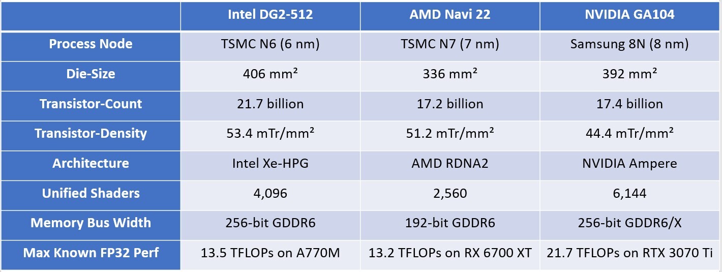
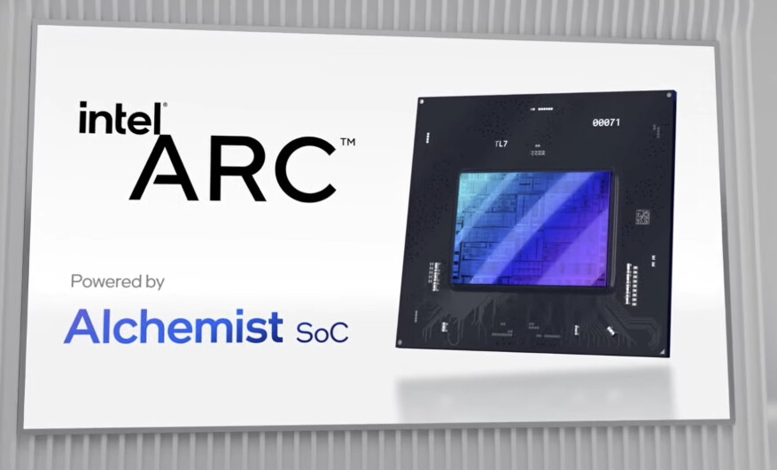
Intel Arc DG2-512 Built on TSMC 6nm, Has More Transistors than GA104 and Navi 22
Some interesting technical specifications of the elusive two GPUs behind the Intel Arc "Alchemist" series surfaced. The larger DG2-512 silicon in particular, which forms the base for the Arc 5 and Arc 7 series, is interesting, in that it is larger in every way than the performance-segment ASICs from both NVIDIA and AMD. The table below compares the physical specs of the DG2-512, with the NVIDIA GA104, and the AMD Navi 22. This segment of GPUs has fairly powerful use-cases, including native 1440p gameplay, or playing at 4K with a performance enhancement—something Intel has, in the form of the XeSS.
The DG2-512 is built on the 6 nm TSMC N6 foundry node, the most advanced node among the three GPUs in this class. It has the highest transistor density of 53.4 mTr/mm², and the largest die-area of 406 mm², and the highest transistor-count of 21.7 billion. The Xe-HPG graphics architecture is designed for full DirectX 12 Ultimate feature support, and the DG2-512 dedicated hardware for ray tracing, as well as AI acceleration. The Arc A770M is the fastest product based on this silicon, however, it is a mobile GPU with aggressive power-management characteristic to the form-factor it serves. Here, the DG2-512 has an FP32 throughput of 13.5 TFLOPs, compared to 13.2 TFLOPs of the Navi 22 on the Radeon RX 6700 XT desktop graphics card, and the 21.7 TFLOPs of the GA104 that's maxed out on the GeForce RTX 3070 Ti desktop graphics card.
The DG2-512 is built on the 6 nm TSMC N6 foundry node, the most advanced node among the three GPUs in this class. It has the highest transistor density of 53.4 mTr/mm², and the largest die-area of 406 mm², and the highest transistor-count of 21.7 billion. The Xe-HPG graphics architecture is designed for full DirectX 12 Ultimate feature support, and the DG2-512 dedicated hardware for ray tracing, as well as AI acceleration. The Arc A770M is the fastest product based on this silicon, however, it is a mobile GPU with aggressive power-management characteristic to the form-factor it serves. Here, the DG2-512 has an FP32 throughput of 13.5 TFLOPs, compared to 13.2 TFLOPs of the Navi 22 on the Radeon RX 6700 XT desktop graphics card, and the 21.7 TFLOPs of the GA104 that's maxed out on the GeForce RTX 3070 Ti desktop graphics card.

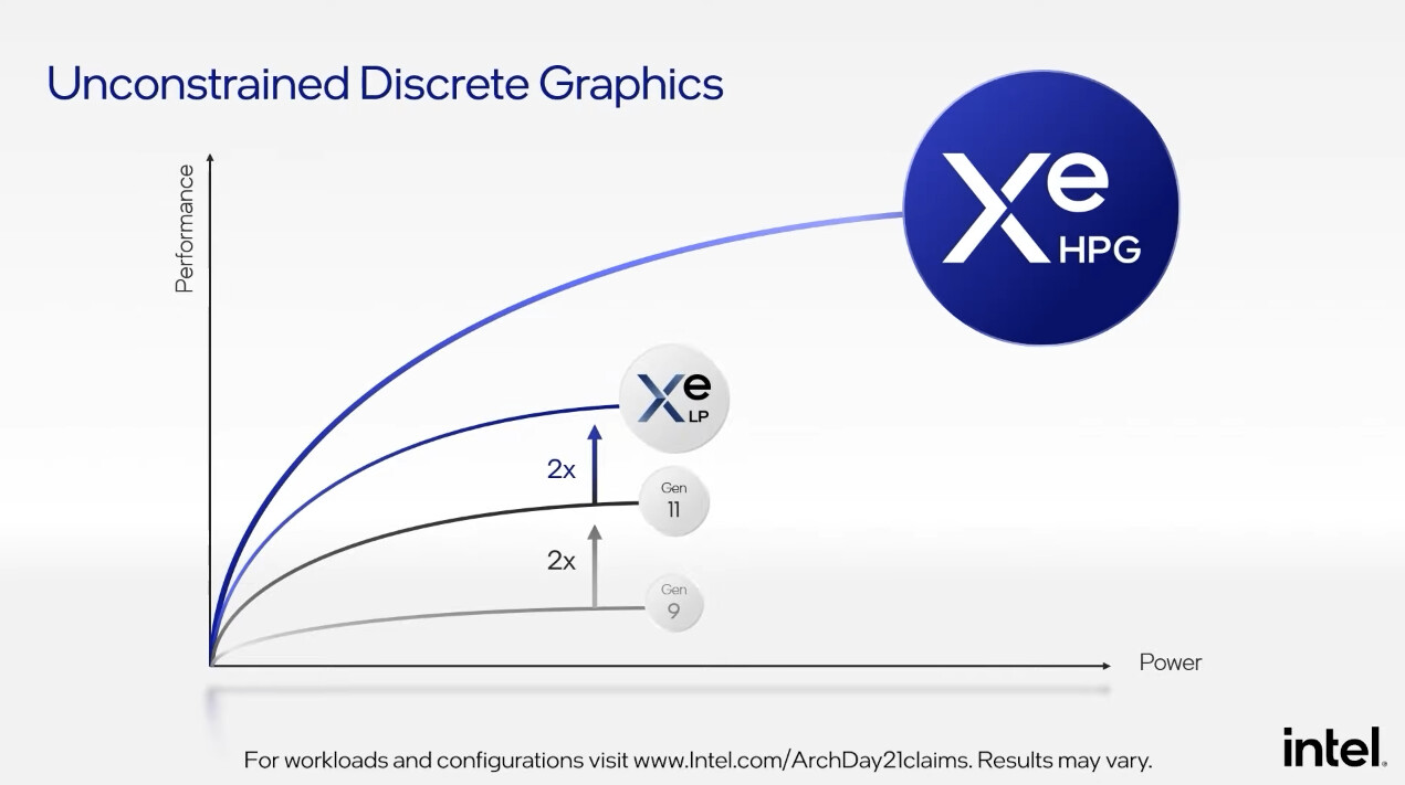
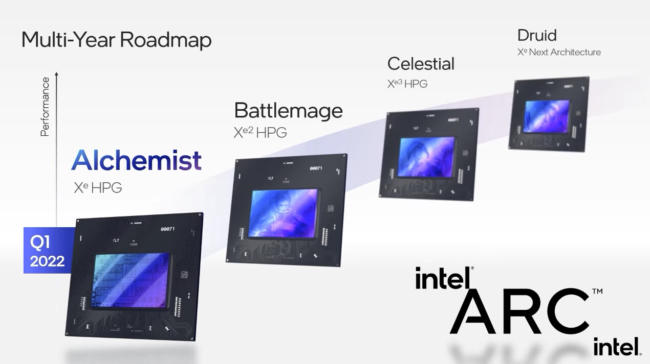
Intel Beats AMD to 6nm GPUs, Arc "Alchemist" Built on TSMC N6 Process
In its 2021 Architecture Day presentation, Intel revealed that its first performance gaming GPU, the Arc "Alchemist," is built on the TSMC N6 silicon fabrication node (6 nm). A more advanced node than the N7 (7 nm) used by AMD for its current RDNA2 GPUs, TSMC N6 leverages EUV (extreme ultraviolet) lithography, and offers 18% higher transistor density, besides power improvements. "With N6, TSMC provides an optimal balance of performance, density, and power-efficiency that are ideal for modern GPUs," said Dr Kevin Zhang, SVP of Business Development at TSMC.
With working prototypes of "Alchemist" already internally circulating as the "DG2," Intel has beaten AMD to 6 nm. Team Red is reportedly planning optical-shrinks of its RDNA2-based "Navi 22" and "Navi 23" chips to TSMC N6, and assigning them mid-range SKUs in the Radeon RX 7000 series. The company will build two higher-segment RDNA3 GPUs on the more advanced TSMC N5 (5 nm) process, which will release in 2022, and power successors to the RX 6700 series and RX 6800/6900 series.


With working prototypes of "Alchemist" already internally circulating as the "DG2," Intel has beaten AMD to 6 nm. Team Red is reportedly planning optical-shrinks of its RDNA2-based "Navi 22" and "Navi 23" chips to TSMC N6, and assigning them mid-range SKUs in the Radeon RX 7000 series. The company will build two higher-segment RDNA3 GPUs on the more advanced TSMC N5 (5 nm) process, which will release in 2022, and power successors to the RX 6700 series and RX 6800/6900 series.

MediaTek Announces Dimensity 920 and Dimensity 810 Chips for 5G Smartphones
MediaTek today announced the new Dimensity 920 and Dimensity 810 chipsets, the latest additions to its Dimensity 5G family. This debut gives smartphone makers the ability to provide boosted performance, brilliant imaging and smarter displays to their customers.
Designed for powerful 5G smartphones, the Dimensity 920 balances performance, power and cost to provide an incredible mobile experience. Built using the 6nm high-performance manufacturing node, it supports intelligent displays and hardware-based 4K HDR video capture, while also offering a 9% boost in gaming performance compared to its predecessor, the Dimensity 900.
Designed for powerful 5G smartphones, the Dimensity 920 balances performance, power and cost to provide an incredible mobile experience. Built using the 6nm high-performance manufacturing node, it supports intelligent displays and hardware-based 4K HDR video capture, while also offering a 9% boost in gaming performance compared to its predecessor, the Dimensity 900.

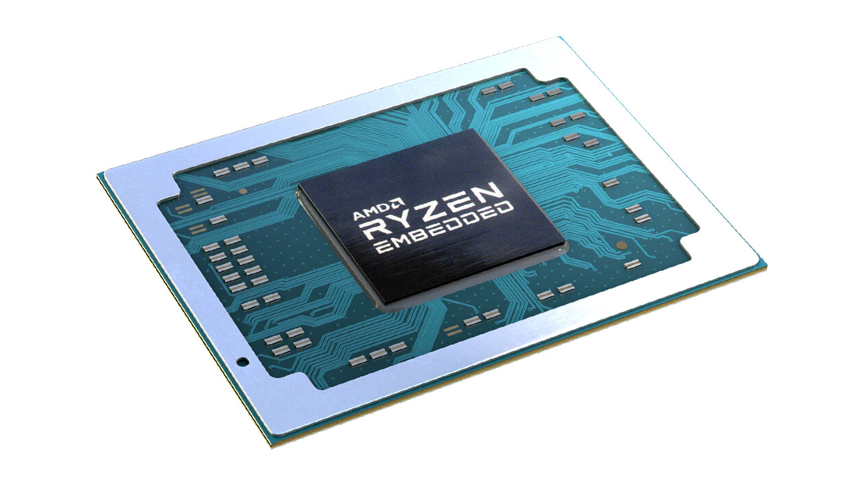
AMD Ryzen Embedded V3000 SoCs Based on 6nm Node, Zen 3 Microarchitecture
AMD's next generation Ryzen Embedded V3000 system-on-chips aren't simply "Cezanne" dies sitting on BGA packages, but rather based on a brand new silicon, according to Patrick Schur, a reliable source with leaks. The die will be built on the more advanced 6 nm silicon fabrication node, whilst still being based on the current "Zen 3" microarchitecture. There are several things that set it apart from the APU silicon of the current-generation, making it more relevant for the applications the Ryzen Embedded processor family is originally built for.
Built in the FP7r2 BGA package, the V3000 silicon features an 8-core/16-thread CPU based on the "Zen 3" microarchitecture. There are also an integrated GPU based on the RDNA2 graphics architecture, with up to 12 CUs, a dual-channel DDR5 memory interface, a 20-lane PCI-Express 4.0 root complex, with up to 8 lanes put out for PEG; two USB4 ports, and two 10 GbE PHYs. AMD could design at least three SKUs based on this silicon, spanning TDP bands of 15-30 W and 35-54 W.
Built in the FP7r2 BGA package, the V3000 silicon features an 8-core/16-thread CPU based on the "Zen 3" microarchitecture. There are also an integrated GPU based on the RDNA2 graphics architecture, with up to 12 CUs, a dual-channel DDR5 memory interface, a 20-lane PCI-Express 4.0 root complex, with up to 8 lanes put out for PEG; two USB4 ports, and two 10 GbE PHYs. AMD could design at least three SKUs based on this silicon, spanning TDP bands of 15-30 W and 35-54 W.
MediaTek Announces New 6nm Dimensity 900 5G Chipset
MediaTek today announced the new Dimensity 900 5G chipset, the latest addition to its Dimensity 5G family. The Dimensity 900 chipset, built on the 6nm high-performance manufacturing node, supports Wi-Fi 6 connectivity, ultra-fast FHD+ 120Hz displays and a 108MP main camera for an all-around incredible experience. "Dimensity 900 brings a suite of connectivity, display and 4K HDR visual enhancements to high-tier 5G smartphones and gives brands great design flexibility for their 5G portfolios," said Dr. JC Hsu, Corporate VP and GM of MediaTek's Wireless Communications Business Unit. "The chipset's support for 5G and Wi-Fi 6 ensures users get the most of out their devices with super-fast and reliable connectivity."
The Dimensity 900 chipset is integrated with a 5G New Radio (NR) sub-6GHz modem with carrier aggregation and support for bandwidth up to 120 MHz. The chipset is equipped with an 8-core central processing unit (CPU) consisting of two Arm Cortex-A78 processors with a clock speed of up to 2.4 GHz and six Arm Cortex-A55 cores operating at up to 2.00 GHz. Dimensity 900 supports flagship LPDDR5 memory and UFS 3.1 storage, and can adapt to a 120 Hz screen refresh rate, bringing excellent performance improvements and a seamless experience to 5G mobile devices.
The Dimensity 900 chipset is integrated with a 5G New Radio (NR) sub-6GHz modem with carrier aggregation and support for bandwidth up to 120 MHz. The chipset is equipped with an 8-core central processing unit (CPU) consisting of two Arm Cortex-A78 processors with a clock speed of up to 2.4 GHz and six Arm Cortex-A55 cores operating at up to 2.00 GHz. Dimensity 900 supports flagship LPDDR5 memory and UFS 3.1 storage, and can adapt to a 120 Hz screen refresh rate, bringing excellent performance improvements and a seamless experience to 5G mobile devices.

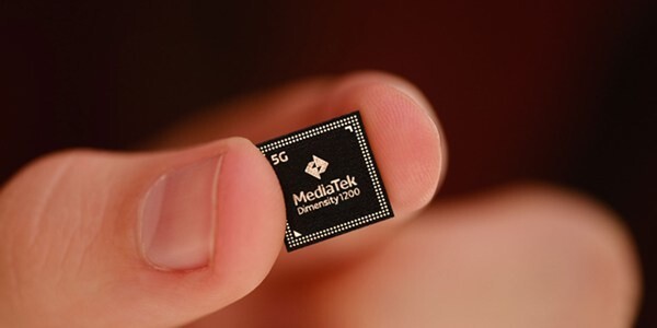
MediaTek Launches 6nm Dimensity 1200 Premium 5G SoC
MediaTek today unveiled its new Dimensity 1200 and Dimensity 1100 5G smartphone chipsets with unrivaled AI, camera and multimedia features for powerful 5G experiences. The addition of the 6 nm Dimensity 1200 and 1100 chipsets to MediaTek's 5G portfolio gives device makers a growing suite of options to design highly capable 5G smartphones with top of the line camera features, graphics, connectivity enhancements and more.
"MediaTek continues to expand its 5G portfolio with highly integrated solutions for a range of devices from the high-end to the mid-tier," said JC Hsu, Corporate Vice President and General Manager of MediaTek's Wireless Communications Business Unit. "Our new Dimensity 1200 stands out with its impressive 200MP camera support and advanced AI capabilities, in addition to its innovative connectivity, display, audio and gaming enhancements."
"MediaTek continues to expand its 5G portfolio with highly integrated solutions for a range of devices from the high-end to the mid-tier," said JC Hsu, Corporate Vice President and General Manager of MediaTek's Wireless Communications Business Unit. "Our new Dimensity 1200 stands out with its impressive 200MP camera support and advanced AI capabilities, in addition to its innovative connectivity, display, audio and gaming enhancements."
Intel Courts TSMC 6nm and 3nm Nodes for Future Xe GPU Generations
Intel is rumored to be aligning its future-generation Xe GPU development with TSMC's node development cycle, with the company reportedly negotiating with the Taiwanese foundry for 6 nm and 3 nm allocation for its large Xe GPUs. Intel's first Xe discrete GPUs for the market, however, are reportedly built on the company's own 10 nm+ silicon fabrication process.
While Intel's fascination with TSMC 3 nm is understandable, seeking out TSMC's 6 nm node raises eyebrows. Internally referred to as "N6," the 6 nm silicon fabrication node at TSMC is expected to go live either towards the end of 2020 or early 2021, which is when Intel's 10 nm+ node is expected to pick up volume production, beginning with the company's "Tiger Lake" processors. Perhaps a decision has been made internally to ensure that Xe doesn't eat too much into Intel's own foundry capacities meant for processor manufacturing, and to instead outsource Xe manufacturing to third-party foundries like TSMC and Samsung eventually. Way back in April 2019 it was rumored that Intel was evaluating Samsung as a foundry partner for Xe.
While Intel's fascination with TSMC 3 nm is understandable, seeking out TSMC's 6 nm node raises eyebrows. Internally referred to as "N6," the 6 nm silicon fabrication node at TSMC is expected to go live either towards the end of 2020 or early 2021, which is when Intel's 10 nm+ node is expected to pick up volume production, beginning with the company's "Tiger Lake" processors. Perhaps a decision has been made internally to ensure that Xe doesn't eat too much into Intel's own foundry capacities meant for processor manufacturing, and to instead outsource Xe manufacturing to third-party foundries like TSMC and Samsung eventually. Way back in April 2019 it was rumored that Intel was evaluating Samsung as a foundry partner for Xe.

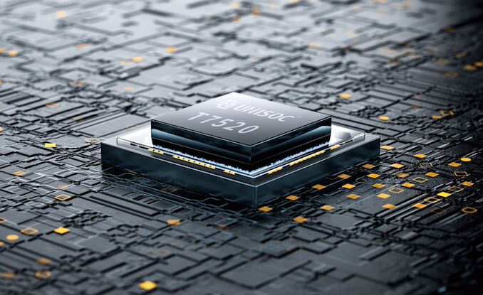
UNISOC Launches Next-Gen 5G SoC T7520 on 6 nm EUV Manufacturing Node
UNISOC, a leading global supplier of mobile communication and IoT chipsets, today officially launched its new-generation 5G SoC mobile platform - T7520. Using cutting-edge process technology, T7520 enables an optimized 5G experience with substantially enhanced AI computing and multimedia imaging processing capabilities while lowering power consumption.
T7520 is UNISOC's second-generation 5G smartphone platform. Built on a 6 nm EUV process technology and empowered by some of the latest design techniques, it offers substantially enhanced performance at a lower level of power consumption than ever.
T7520 is UNISOC's second-generation 5G smartphone platform. Built on a 6 nm EUV process technology and empowered by some of the latest design techniques, it offers substantially enhanced performance at a lower level of power consumption than ever.

TSMC Starts Shipping its 7nm+ Node Based on EUV Technology
TSMC today announced that its seven-nanometer plus (N7+), the industry's first commercially available Extreme Ultraviolet (EUV) lithography technology, is delivering customer products to market in high volume. The N7+ process with EUV technology is built on TSMC's successful 7 nm node and paves the way for 6 nm and more advanced technologies.
The N7+ volume production is one of the fastest on record. N7+, which began volume production in the second quarter of 2019, is matching yields similar to the original N7 process that has been in volume production for more than one year.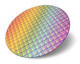
The N7+ volume production is one of the fastest on record. N7+, which began volume production in the second quarter of 2019, is matching yields similar to the original N7 process that has been in volume production for more than one year.

AMD Designing Zen 4 for 2021, Zen 3 Completes Design Phase, out in 2020
AMD in its 2nd generation EPYC processor launch event announced that it has completed the design phase of its next-generation "Zen 3" CPU microarchitecture, and is currently working on its successor, the "Zen 4." AMD debuted its "Zen 2" microarchitecture with the client-segment 3rd generation Ryzen desktop processor family, it made its enterprise debut with the 2nd generation EPYC. This is the first x86 CPU microarchitecture designed for the 7 nanometer silicon fabrication process, and is being built on a 7 nm DUV (deep ultraviolet) node at TSMC. It brings about double-digit percentage IPC improvements over "Zen+."
The "Zen 3" microarchitecture is designed for the next big process technology change within 7 nm, EUV (extreme ultraviolet), which allows significant increases in transistor densities, and could facilitate big improvements in energy-efficiency that could be leveraged to increase clock-speeds and performance. It could also feature new ISA instruction-sets. With "Zen 3" passing design phase, AMD will work on prototyping and testing it. The first "Zen 3" products could debut in 2020. "Zen 4" is being designed for a different era.
The "Zen 3" microarchitecture is designed for the next big process technology change within 7 nm, EUV (extreme ultraviolet), which allows significant increases in transistor densities, and could facilitate big improvements in energy-efficiency that could be leveraged to increase clock-speeds and performance. It could also feature new ISA instruction-sets. With "Zen 3" passing design phase, AMD will work on prototyping and testing it. The first "Zen 3" products could debut in 2020. "Zen 4" is being designed for a different era.


Samsung Announces Breakthrough in Building Blocks of 3nm Circuits, Updates Roadmap
Samsung Electronics Co., Ltd., a world leader in advanced semiconductor technology, today announced its ongoing commitment to foundry innovation and service at the Samsung Foundry Forum 2019 USA, providing the silicon community with wide-ranging updates on technology advances that support the most demanding applications of today and tomorrow.
The event, held today in Santa Clara, California, features top Samsung executives and industry experts reviewing progress on semiconductor technologies and foundry platform solutions that enable developments in artificial intelligence (AI), machine learning, 5G networking, automotive, the Internet of Things (IoT), advanced data centers and many other domains.
The event, held today in Santa Clara, California, features top Samsung executives and industry experts reviewing progress on semiconductor technologies and foundry platform solutions that enable developments in artificial intelligence (AI), machine learning, 5G networking, automotive, the Internet of Things (IoT), advanced data centers and many other domains.

TSMC Unveils 6-nanometer Process
TSMC today announced its 6-nanometer (N6) process, which provides a significant enhancement of its industry-leading N7 technology and offers customers a highly competitive performance-to-cost advantage as well as fast time-to-market with direct migration from N7-based designs. By leveraging the new capabilities in extreme ultraviolet (EUV) lithography gained from the N7+ technology currently in risk production, TSMC's N6 process delivers 18% higher logic density over the N7 process. At the same time, its design rules are fully compatible with TSMC's proven N7 technology, allowing its comprehensive design ecosystem to be reused. As a result, it offers a seamless migration path with a fast design cycle time with very limited engineering resources for customers to achieve the product benefits from the new technology offering.
Scheduled for risk production in the first quarter of 2020, TSMC's N6 technology provides customers with additional cost-effective benefits while extending the industry-leading power and performance from the 7nm family for a broad array of applications, ranging from high-to-mid end mobile, consumer applications, AI, networking, 5G infrastructure, GPU, and high-performance computing.
Scheduled for risk production in the first quarter of 2020, TSMC's N6 technology provides customers with additional cost-effective benefits while extending the industry-leading power and performance from the 7nm family for a broad array of applications, ranging from high-to-mid end mobile, consumer applications, AI, networking, 5G infrastructure, GPU, and high-performance computing.
Apr 16th, 2025 08:52 EDT
change timezone
Latest GPU Drivers
New Forum Posts
- Last game you purchased? (771)
- GPU Memory Temprature is always high (16)
- Windows 11 fresh install to do list (20)
- 5070ti overclock...what are your settings? (3)
- Help For XFX RX 590 GME Chinese - Vbios (4)
- PCGH: "hidden site" to see total money spend on steam (3)
- Share your AIDA 64 cache and memory benchmark here (3053)
- NVFlash for RTX 50 Series (Blackwell) (0)
- intel 1700 with high speed ram,memory (63)
- The TPU UK Clubhouse (26115)
Popular Reviews
- G.SKILL Trident Z5 NEO RGB DDR5-6000 32 GB CL26 Review - AMD EXPO
- ASUS GeForce RTX 5080 TUF OC Review
- DAREU A950 Wing Review
- The Last Of Us Part 2 Performance Benchmark Review - 30 GPUs Compared
- Sapphire Radeon RX 9070 XT Pulse Review
- Sapphire Radeon RX 9070 XT Nitro+ Review - Beating NVIDIA
- Upcoming Hardware Launches 2025 (Updated Apr 2025)
- Thermaltake TR100 Review
- Zotac GeForce RTX 5070 Ti Amp Extreme Review
- TerraMaster F8 SSD Plus Review - Compact and quiet
Controversial News Posts
- NVIDIA GeForce RTX 5060 Ti 16 GB SKU Likely Launching at $499, According to Supply Chain Leak (182)
- NVIDIA Sends MSRP Numbers to Partners: GeForce RTX 5060 Ti 8 GB at $379, RTX 5060 Ti 16 GB at $429 (124)
- Nintendo Confirms That Switch 2 Joy-Cons Will Not Utilize Hall Effect Stick Technology (105)
- Over 200,000 Sold Radeon RX 9070 and RX 9070 XT GPUs? AMD Says No Number was Given (100)
- Nintendo Switch 2 Launches June 5 at $449.99 with New Hardware and Games (99)
- Sony Increases the PS5 Pricing in EMEA and ANZ by Around 25 Percent (85)
- NVIDIA PhysX and Flow Made Fully Open-Source (77)
- NVIDIA Pushes GeForce RTX 5060 Ti Launch to Mid-April, RTX 5060 to May (77)