News Posts matching #Arctic Islands

Return to Keyword Browsing

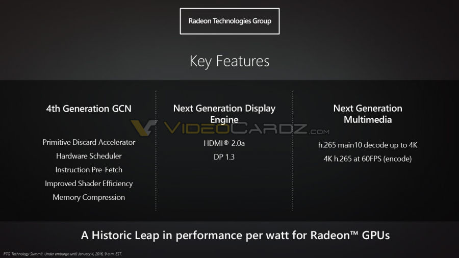
4th Generation Graphics CoreNext Architecture Codenamed "Polaris"

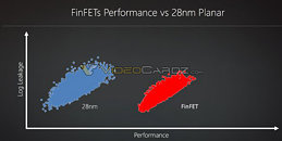
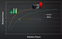
The fourth generation of AMD Graphics CoreNext GPU architecture has been reportedly codenamed "Polaris" by the company. It makes its debut later this year in the company's "Arctic Islands" GPUs, built on Samsung's 14 nm FinFET node. According to the company, Polaris will provide a "historic leap in performance/Watt" for Radeon GPUs. Chips based on Polaris will feature improvements to not just the compute units, but will also come with generational improvements to pretty much every other component, including a new front-end, display controllers, and a new memory controller supporting HBM2.

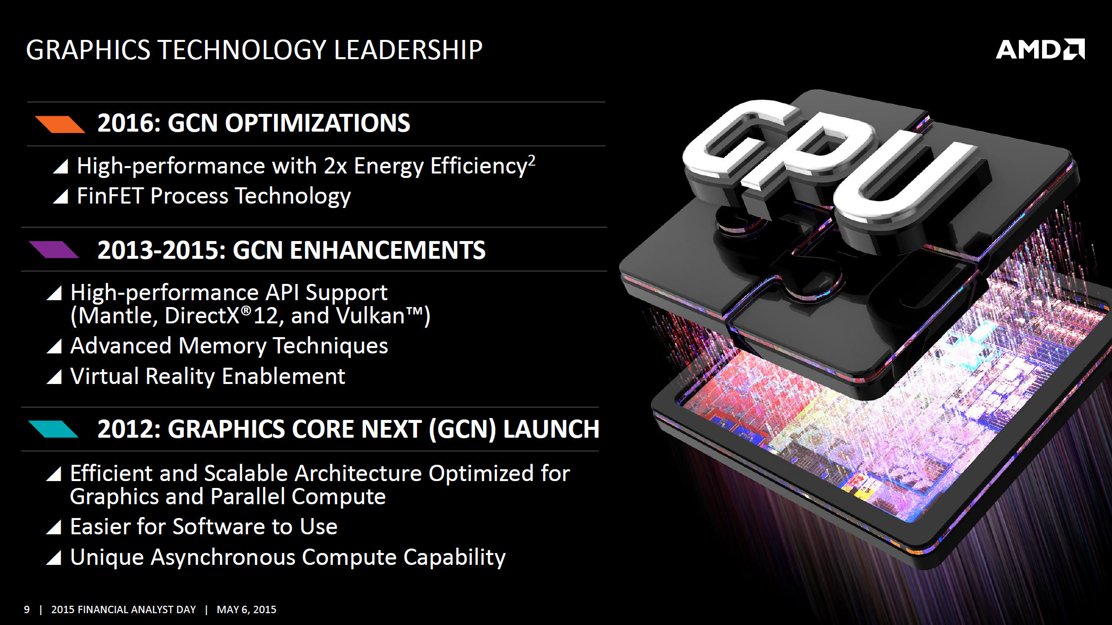
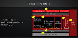
AMD debuted its first generation GCN architecture with the Radeon HD 7000 series, notably the "Tahiti" silicon. Its second-generation, GCN 2.0, (reported in the press as GCN 1.1), debuted with the R9 290 series, notably the "Hawaii" silicon. The third-generation, GCN 3.0 (reported in the press as GCN 1.2), debuted with the R9 285, notably the "Tonga" silicon; making "Polaris" the fourth-generation. GCN 4.0 will form the core micro-architecture of the "Arctic Islands" family of GPUs, which make their debut in mid-2016.

Samsung to Fab AMD "Zen" and "Arctic Islands" on its 14 nm FinFET Node

It has been confirmed that Samsung will be AMD's foundry partner for its next generation GPUs. It has been reported that AMD's upcoming "Arctic Islands" family of GPUs could be built on the 14 nanometer FinFET LPP (low-power Plus) process. AMD's rival NVIDIA, meanwhile, is building its next-gen "Pascal" GPU family on 16 nanometer FinFET node, likely at its traditional foundry partner TSMC.

It gets better - not only will Samsung manufacture AMD's next-gen GPUs, but also its upcoming "Zen" family of CPUs, at least a portion of it. AMD is looking to distribute manufacturing loads between two foundries, Samsung and GlobalFoundries, perhaps to ensure that foundry-level teething trouble doesn't throw its product launch cycle off the rails. One of the most talked about "Arctic Islands" GPUs is codenamed "Greenland," likely a successor to "Fiji." Sales of some of the first chips - GPUs or CPUs - made at Samsung, will begin some time in Q3 2016. Some of the other clients for Samsung's 14 nm FinFET node are Apple and Qualcomm. The company plans to speed up development of its more advanced 10 nm node to some time in 2017.

Next Gen AMD GPUs to Get a Massive Energy Efficiency Design Focus

AMD's upcoming generations of GPUs will get a massive design focus on energy-efficiency and increases in performance-per-Watt, according to a WCCFTech report. The first of these chips, codenamed "Arctic Islands," will leverage cutting edge 10 nm-class FinFET silicon fab technology, coupled with bare-metal and software optimization to step up performance-per-Watt in a big way. The last time AMD achieved an energy efficiency leap was with the Radeon HD 5000 series (helped in part by abysmal energy efficiency of the rivaling GeForce GTX 400 series).

GlobalFoundries 14 nm LPP FinFET Node Taped Out, Yields Good

GlobalFoundries' move to leapfrog several silicon fab steps to get straight to 14 nanometer (nm) is on the verge of paying off, with the company taping out its 14 nm LPP (low-power plus) FinFET node, and claiming good yields on its test/QA chips. This takes the node one step closer to accepting orders for manufacturing of extremely complex chips, such as CPUs and GPUs.

AMD is expected to remain the company's biggest client, with plans to build its next-generation "Zen" processor on this node. The company's "Arctic Islands" graphics chips are also rumored to be built on the 14 nm node, although which foundry will handle its mass production remains unclear. A big chunk of AMD's R&D budget is allocated to getting the "Zen" architecture right, with key stages of its development being handled by Jim Keller, the brains behind some of AMD's most commercially successful CPU cores.

AMD to Skip 20 nm, Jump Straight to 14 nm with "Arctic Islands" GPU Family

AMD's next-generation GPU family, which it plans to launch some time in 2016, codenamed "Arctic Islands," will see the company skip the 20 nanometer silicon fab process from 28 nm, and jump straight to 14 nm FinFET. Whether the company will stick with TSMC, which is seeing crippling hurdles to implement its 20 nm node for GPU vendors; or hire a new fab, remains to be seen. Intel and Samsung are currently the only fabs with 14 nm nodes that have attained production capacity. Intel is manufacturing its Core "Broadwell" CPUs, while Samsung is manufacturing its Exynos 7 (refresh) SoCs. Intel's joint-venture with Micron Technology, IMFlash, is manufacturing NAND flash chips on 14 nm.

Named after islands in the Arctic circle, and a possible hint at the low TDP of the chips, benefiting from 14 nm, "Arctic Islands" will be led by "Greenland," a large GPU that will implement the company's most advanced stream processor design, and implement HBM2 memory, which offers 57% higher memory bandwidth at just 48% the power consumption of GDDR5. Korean memory manufacturer SK Hynix is ready with its HBM2 chip designs.
Return to Keyword Browsing
Jul 15th, 2024 23:25 EDT change timezone

New Forum Posts

Popular Reviews

Controversial News Posts