HBM Industry Revenue Could Double by 2025 - Growth Driven by Next-gen AI GPUs Cited
Samsung, SK hynix, and Micron are considered to be the top manufacturing sources of High Bandwidth Memory (HBM)—the HBM3 and HBM3E standards are becoming increasingly in demand, due to a widespread deployment of GPUs and accelerators by generative AI companies. Taiwan's Commercial Times proposes that there is an ongoing shortage of HBM components—but this presents a growth opportunity for smaller manufacturers in the region. Naturally, the big name producers are expected to dive in head first with the development of next generation models. The aforementioned financial news article cites research conducted by the Gartner group—they predict that the HBM market will hit an all-time high of $4.976 billion (USD) by 2025.
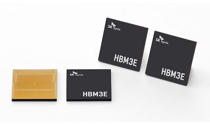
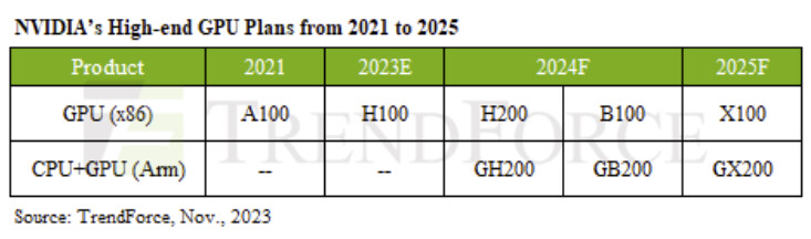
This estimate is almost double that of projected revenues (just over $2 billion) generated by the HBM market in 2023—the explosive growth of generative AI applications has "boosted" demand for the most performant memory standards. The Commercial Times report states that SK Hynix is the current HBM3E leader, with Micron and Samsung trailing behind—industry experts believe that stragglers will need to "expand HBM production capacity" in order to stay competitive. SK Hynix has shacked up with NVIDIA—the GH200 Grace Hopper platform was unveiled last summer; outfitted with the South Korean firm's HBM3e parts. In a similar timeframe, Samsung was named as AMD's preferred supplier of HBM3 packages—as featured within the recently launched Instinct MI300X accelerator. NVIDIA's HBM3E deal with SK Hynix is believed to extend to the internal makeup of Blackwell GB100 data-center GPUs. The HBM4 memory standard is expected to be the next major battleground for the industry's hardest hitters.


This estimate is almost double that of projected revenues (just over $2 billion) generated by the HBM market in 2023—the explosive growth of generative AI applications has "boosted" demand for the most performant memory standards. The Commercial Times report states that SK Hynix is the current HBM3E leader, with Micron and Samsung trailing behind—industry experts believe that stragglers will need to "expand HBM production capacity" in order to stay competitive. SK Hynix has shacked up with NVIDIA—the GH200 Grace Hopper platform was unveiled last summer; outfitted with the South Korean firm's HBM3e parts. In a similar timeframe, Samsung was named as AMD's preferred supplier of HBM3 packages—as featured within the recently launched Instinct MI300X accelerator. NVIDIA's HBM3E deal with SK Hynix is believed to extend to the internal makeup of Blackwell GB100 data-center GPUs. The HBM4 memory standard is expected to be the next major battleground for the industry's hardest hitters.