News Posts matching #Imec

Return to Keyword Browsing

Imec Demonstrates Logic and DRAM Structures Using High NA EUV Lithography

Imec, a world-leading research and innovation hub in nanoelectronics and digital technologies, presents patterned structures obtained after exposure with the 0.55NA EUV scanner in the joint ASML-imec High NA EUV Lithography Lab in Veldhoven, the Netherlands. Random logic structures down to 9,5 nm (19 nm pitch), random vias with 30 nm center-to-center distance, 2D features at 22 nm pitch, and a DRAM specific lay out at P32nm were printed after single exposure, using materials and baseline processes that were optimized for High NA EUV by imec and its partners in the framework of imec's Advanced Patterning Program. With these results, imec confirms the readiness of the ecosystem to enable single exposure high-resolution High NA EUV Lithography.

Following the recent opening of the joint ASML-imec High NA EUV Lithography Lab in Veldhoven, the Netherlands, customers now have access to the (TWINSCAN EXE:5000) High NA EUV scanner to develop private High NA EUV use cases leveraging the customer's own design rules and lay outs.

Imec Develops Ultra-Low Noise Si MOS Quantum Dots Using 300mm CMOS Technology

Imec, a world-leading research and innovation hub in nanoelectronics and digital technologies, today announced the demonstration of high quality 300 mm-Si-based quantum dot spin qubit processing with devices resulting in a statistically relevant, average charge noise of 0.6µeV/√ Hz at 1 Hz. In view of noise performance, the values obtained are the lowest charge noise values achieved on a 300 mm fab-compatible platform.

Such low noise values enable high-fidelity qubit control, as reducing the noise is critical for maintaining quantum coherence and high fidelity control. By demonstrating those values, repeatedly and reproducibly, on a 300 mm Si MOS quantum dot process, this work makes large-scale quantum computers based on Si quantum dots a realistic possibility.

ASML CTO Expects Post High-NA Lithography to be Prohibitively Costly

In an interview with Bits & Chips, ASML's CTO Martin van den Brink said that he believes that we might be reaching the end of the road for current semiconductor lithography technology in the not so distant future. However, for the time being, ASML is executing on its roadmap and after EUV, the next step is high-NA or high-numerical aperture and ASML is currently planning to have its first research high-NA scanner ready for a joint R&D venture with Imec in 2023. Assuming everything goes to plan, ASML is then planning on delivering the first R&D machines to its customers in 2024, followed by deliver of the first volume production machines using high-NA sometime in 2025. Van den Brink points out that due to the current supply chain uncertainties could affect the timing, in combination with the fact that ASML has a high demand for its EUV machines and the two technologies share a lot of components.

As such, current orders are the priority and high-NA development might be put on the back burner if need be, or as Van den Brink puts it "today's meal takes priority over tomorrow's." High-NA scanners are expected to be even more power hungry than EUV machines and are as such expected to pull around two Megawatts for the various stages. The next step in the evolution of semiconductor lithography is where ASML is expecting things to get problematic, as what the company is currently calling hyper-NA is expected to be prohibitively costly to manufacture and use. If the cost of hyper-NA grows as fast as we've seen in high-NA, it will pretty much be economically unfeasible," Van den Brink said. ASML is hoping to overcome the cost issues, but for now, the company has a plan for the next decade and things could very well change during that time and remove some of the obstacles that are currently being seen.

Imec and GLOBALFOUNDRIES Announce Breakthrough in AI Chip on IoT Edge Devices

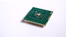
Imec, a world-leading research and innovation hub in nanoelectronics and digital technologies, and GLOBALFOUNDRIES (GF ), the world's leading specialty foundry, today announced a hardware demonstration of a new artificial intelligence chip. Based on imec's Analog in Memory Computing (AiMC) architecture utilizing GF's 22FDX solution, the new chip is optimized to perform deep neural network calculations on in-memory computing hardware in the analog domain. Achieving record-high energy efficiency up to 2,900 TOPS/W, the accelerator is a key enabler for inference-on-the-edge for low-power devices. The privacy, security and latency benefits of this new technology will have an impact on AI applications in a wide range of edge devices, from smart speakers to self-driving vehicles.
Return to Keyword Browsing
Dec 30th, 2024 12:16 EST change timezone

New Forum Posts

Popular Reviews

Controversial News Posts