Apr 16th, 2025 08:53 EDT
change timezone
Latest GPU Drivers
New Forum Posts
- Last game you purchased? (771)
- GPU Memory Temprature is always high (16)
- Windows 11 fresh install to do list (20)
- 5070ti overclock...what are your settings? (3)
- Help For XFX RX 590 GME Chinese - Vbios (4)
- PCGH: "hidden site" to see total money spend on steam (3)
- Share your AIDA 64 cache and memory benchmark here (3053)
- NVFlash for RTX 50 Series (Blackwell) (0)
- intel 1700 with high speed ram,memory (63)
- The TPU UK Clubhouse (26115)
Popular Reviews
- G.SKILL Trident Z5 NEO RGB DDR5-6000 32 GB CL26 Review - AMD EXPO
- ASUS GeForce RTX 5080 TUF OC Review
- DAREU A950 Wing Review
- The Last Of Us Part 2 Performance Benchmark Review - 30 GPUs Compared
- Sapphire Radeon RX 9070 XT Pulse Review
- Sapphire Radeon RX 9070 XT Nitro+ Review - Beating NVIDIA
- Upcoming Hardware Launches 2025 (Updated Apr 2025)
- Thermaltake TR100 Review
- Zotac GeForce RTX 5070 Ti Amp Extreme Review
- TerraMaster F8 SSD Plus Review - Compact and quiet
Controversial News Posts
- NVIDIA GeForce RTX 5060 Ti 16 GB SKU Likely Launching at $499, According to Supply Chain Leak (182)
- NVIDIA Sends MSRP Numbers to Partners: GeForce RTX 5060 Ti 8 GB at $379, RTX 5060 Ti 16 GB at $429 (124)
- Nintendo Confirms That Switch 2 Joy-Cons Will Not Utilize Hall Effect Stick Technology (105)
- Over 200,000 Sold Radeon RX 9070 and RX 9070 XT GPUs? AMD Says No Number was Given (100)
- Nintendo Switch 2 Launches June 5 at $449.99 with New Hardware and Games (99)
- Sony Increases the PS5 Pricing in EMEA and ANZ by Around 25 Percent (85)
- NVIDIA PhysX and Flow Made Fully Open-Source (77)
- NVIDIA Pushes GeForce RTX 5060 Ti Launch to Mid-April, RTX 5060 to May (77)
News Posts matching #N1
Return to Keyword BrowsingUltra-compact Morefine M6S Plus Mini PC Set to Launch with Intel Twin Lake Processor
The world of mini PCs keeps on growing, thanks to a boost in popularity made possible by the impressive efficiency and performance improvements brought to the table by the silicon giants, allowing compact systems to function just as well as full-fledged towers. The Morefine M6S Plus is yet another addition to the list of mini PCs, and it appears that the system prioritizes portability and compactness over raw performance. For a sizeable chunk of casual desktop users, even entry-level processors pack enough computing grunt to ease through their workloads, and that demographic is exactly what the M6S Plus targets.
With dimensions of 7.2 x 7.2 x 4.2 cm, the Morefine M6S Plus is commendably compact indeed. As mentioned, the computing horsepower offered is very limited, thanks to the quad-core Intel N150 processor that lacks Hyper-Threading. The memory is, unfortunately, not user upgradeable, so customers are will have to stick the 12 GB of LPDDR5-4800 memory on offer. The storage however, is upgradeable, thanks to the M.2 2242 slot which can accommodate up to 4 TB of storage. In terms of connectivity, the options are acceptable, including dual Type-C ports with DP, gigabit ethernet, triple USB 3.2 Gen 1Type-A ports (two on the front), HDMI 2.1, as well as a headphone jack.

With dimensions of 7.2 x 7.2 x 4.2 cm, the Morefine M6S Plus is commendably compact indeed. As mentioned, the computing horsepower offered is very limited, thanks to the quad-core Intel N150 processor that lacks Hyper-Threading. The memory is, unfortunately, not user upgradeable, so customers are will have to stick the 12 GB of LPDDR5-4800 memory on offer. The storage however, is upgradeable, thanks to the M.2 2242 slot which can accommodate up to 4 TB of storage. In terms of connectivity, the options are acceptable, including dual Type-C ports with DP, gigabit ethernet, triple USB 3.2 Gen 1Type-A ports (two on the front), HDMI 2.1, as well as a headphone jack.


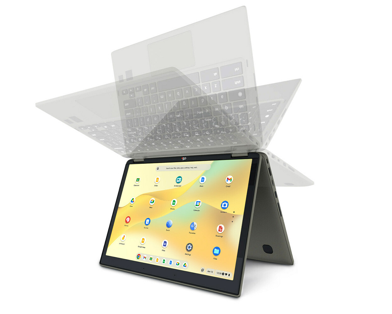
CTL Announces the Chromebook NL73 Series
CTL, a global cloud-computing solution leader for education, announced today the introduction of the new CTL Chromebook NL73 Series. The new Chromebook, incorporating the Intel Processor N100 and Intel Processor N200, enables IT professionals to equip schools with the cloud-computing performance they need today and with the sustainability required for tomorrow.
"Since Chromebooks were widely deployed during the pandemic to remote students, new applications have come into use, requiring more processing power and cybersecurity measures than ever before," noted Erik Stromquist, CEO of CTL. "Chromebook users will need to level up their technology in 2024. Our new NL73 Series delivers not only the power to meet these new requirements but also CTL's flexible configuration options, purchase options, and whole lifecycle management services for the ultimate in sustainability."
"Since Chromebooks were widely deployed during the pandemic to remote students, new applications have come into use, requiring more processing power and cybersecurity measures than ever before," noted Erik Stromquist, CEO of CTL. "Chromebook users will need to level up their technology in 2024. Our new NL73 Series delivers not only the power to meet these new requirements but also CTL's flexible configuration options, purchase options, and whole lifecycle management services for the ultimate in sustainability."

TSMC Plans to Put a Trillion Transistors on a Single Package by 2030
During the recent IEDM conference, TSMC previewed its process roadmap for delivering next-generation chip packages packing over one trillion transistors by 2030. This aligns with similar long-term visions from Intel. Such enormous transistor counts will come through advanced 3D packaging of multiple chipsets. But TSMC also aims to push monolithic chip complexity higher, ultimately enabling 200 billion transistor designs on a single die. This requires steady enhancement of TSMC's planned N2, N2P, N1.4, and N1 nodes, which are slated to arrive between now and the end of the decade. While multi-chipset architectures are currently gaining favor, TSMC asserts both packaging density and raw transistor density must scale up in tandem. Some perspective on the magnitude of TSMC's goals include NVIDIA's 80 billion transistor GH100 GPU—among today's largest chips, excluding wafer-scale designs from Cerebras.
Yet TSMC's roadmap calls for more than doubling that, first with over 100 billion transistor monolithic designs, then eventually 200 billion. Of course, yields become more challenging as die sizes grow, which is where advanced packaging of smaller chiplets becomes crucial. Multi-chip module offerings like AMD's MI300X and Intel's Ponte Vecchio already integrate dozens of tiles, with PVC having 47 tiles. TSMC envisions this expansion to chip packages housing more than a trillion transistors via its CoWoS, InFO, 3D stacking, and many other technologies. While the scaling cadence has recently slowed, TSMC remains confident in achieving both packaging and process breakthroughs to meet future density demands. The foundry's continuous investment ensures progress in unlocking next-generation semiconductor capabilities. But physics ultimately dictates timelines, no matter how aggressive the roadmap.
Yet TSMC's roadmap calls for more than doubling that, first with over 100 billion transistor monolithic designs, then eventually 200 billion. Of course, yields become more challenging as die sizes grow, which is where advanced packaging of smaller chiplets becomes crucial. Multi-chip module offerings like AMD's MI300X and Intel's Ponte Vecchio already integrate dozens of tiles, with PVC having 47 tiles. TSMC envisions this expansion to chip packages housing more than a trillion transistors via its CoWoS, InFO, 3D stacking, and many other technologies. While the scaling cadence has recently slowed, TSMC remains confident in achieving both packaging and process breakthroughs to meet future density demands. The foundry's continuous investment ensures progress in unlocking next-generation semiconductor capabilities. But physics ultimately dictates timelines, no matter how aggressive the roadmap.


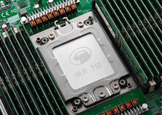
Export Regulations Hinder China's Plans for Custom Arm-Based Processors
The United States has recently imposed several sanctions on technology exports to China. These sanctions are designed to restrict the transfer of specific technologies and sensitive information to Chinese entities, particularly those with ties to the Chinese military or government. The primary motivation behind these sanctions is to protect American national security interests, as well as to protect American companies from unfair competition. According to Financial Times, we have information that Chinese tech Giant, Alibaba, can not access Arm licenses for Neoverse V1 technology. Generally, the technology group where Neoverse V-series falls in is called Wassenaar -- multilateral export control regime (MECR) with 42 participating states. This agreement prohibits the sale of technology that could be used for military purposes.
The US argues that Arm's Neoverse V1 IP is not only a product from UK's Arm but a design made in the US as well, meaning that it is a US technology. Since Alibaba's T-Head group responsible for designing processors that go into Alibaba's cloud services can not use Neoverse V1, it has to look for alternative solutions. The Neoverse V1 and V2 can not be sold in China, while Neoverse N1 and N2 can. Alibaba's T-Head engineer argued, "We feel that the western world sees us as second-class people. They won't sell good products to us even if we have money."
The US argues that Arm's Neoverse V1 IP is not only a product from UK's Arm but a design made in the US as well, meaning that it is a US technology. Since Alibaba's T-Head group responsible for designing processors that go into Alibaba's cloud services can not use Neoverse V1, it has to look for alternative solutions. The Neoverse V1 and V2 can not be sold in China, while Neoverse N1 and N2 can. Alibaba's T-Head engineer argued, "We feel that the western world sees us as second-class people. They won't sell good products to us even if we have money."
TSMC N1 Node Chip Plant Said to be Under Planning
Based on news out of Taiwan, TSMC is said to be in the early planning stages of yet another chip plant, this time for its first N1 node. The new plant will reportedly be built in a science park in Taoyuan, less than an hour south west of Taipei, according to the Commercial Times. TSMC already has a pair of chip packaging and testing facilities in the science park, making it a suitable location for a chip plant. This will be TSMC's most northern chip manufacturing plant in Taiwan, although it's not expected to start pilot production until sometime in 2027. TSMC hasn't confirmed any of the details, but the company didn't outright deny the report either.
Despite the potential global downturn in the economy, TSMC appears to be fully committed to continue to build new fabs for increasingly smaller nodes. The company is set to start its first commercial production on its N3 node this quarter and is expecting the N3 node to contribute as much as four to six percent of its overall revenue in 2023. Its N2 node should enter commercial production in 2025, but not much is known about the state of the N2 node at this point in time. The N1 node might end up being a 1.4 nm node, based on TSMC's measurements, but the company is still in the very beginning of the R&D phase for this node.
Despite the potential global downturn in the economy, TSMC appears to be fully committed to continue to build new fabs for increasingly smaller nodes. The company is set to start its first commercial production on its N3 node this quarter and is expecting the N3 node to contribute as much as four to six percent of its overall revenue in 2023. Its N2 node should enter commercial production in 2025, but not much is known about the state of the N2 node at this point in time. The N1 node might end up being a 1.4 nm node, based on TSMC's measurements, but the company is still in the very beginning of the R&D phase for this node.

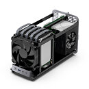
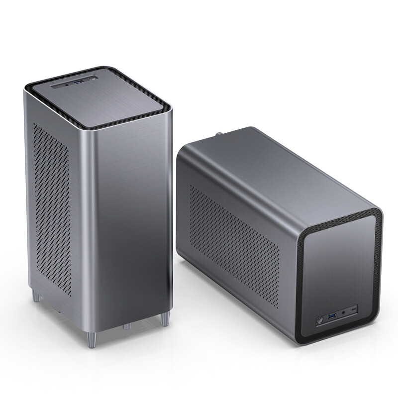
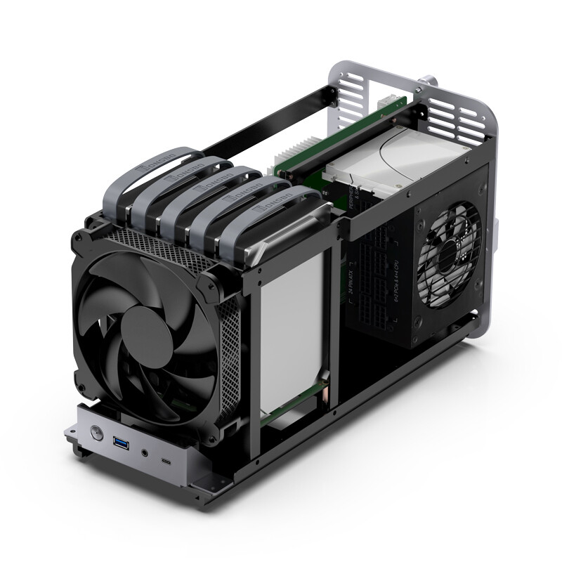
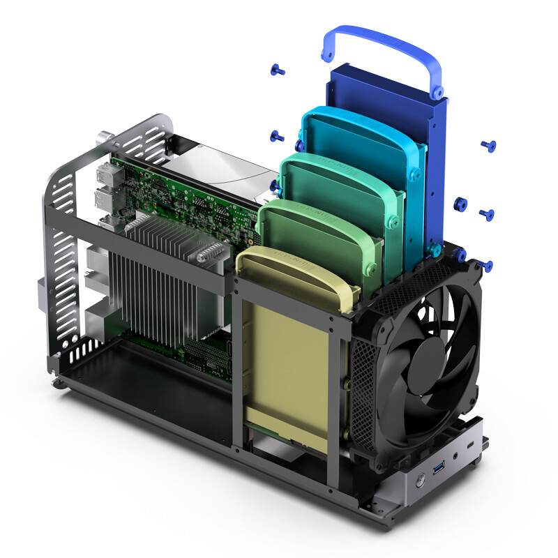
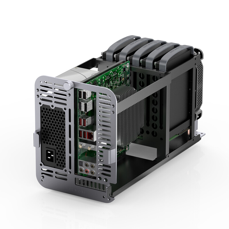
Jonsbo Introduces the N1 Mini-ITX Chassis
Jonsbo has added to their PC case lineup with the introduction of the N1 Mini-ITX chassis. The N1 features a minimalist, industrial design thanks to its external brushed aluminium enclosure (3 mm) and steel innards (1 mm thick), and includes four feet so the tower can be put in vertical position, in addition to its apparently stock, horizontal one. The Jonsbo N1 features 5x 3.5" expansion bays, and 1x low-profile PCIe expansion port.
A single 140 mm fan on the front of the unit helps keep temperatures in check (particularly for the HDDs), and there's naturally support for a SFF power supply (up to 150 mm in length). The CPU cooler has clearance for up to 70 mm, and the graphics card support is limited to 185 mm. The front panel offers 1x USB 3.0, 1x USB Type-C, and 1x audio port. No word on pricing was available at time of writing.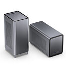

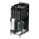

A single 140 mm fan on the front of the unit helps keep temperatures in check (particularly for the HDDs), and there's naturally support for a SFF power supply (up to 150 mm in length). The CPU cooler has clearance for up to 70 mm, and the graphics card support is limited to 185 mm. The front panel offers 1x USB 3.0, 1x USB Type-C, and 1x audio port. No word on pricing was available at time of writing.

Apr 16th, 2025 08:53 EDT
change timezone
Latest GPU Drivers
New Forum Posts
- Last game you purchased? (771)
- GPU Memory Temprature is always high (16)
- Windows 11 fresh install to do list (20)
- 5070ti overclock...what are your settings? (3)
- Help For XFX RX 590 GME Chinese - Vbios (4)
- PCGH: "hidden site" to see total money spend on steam (3)
- Share your AIDA 64 cache and memory benchmark here (3053)
- NVFlash for RTX 50 Series (Blackwell) (0)
- intel 1700 with high speed ram,memory (63)
- The TPU UK Clubhouse (26115)
Popular Reviews
- G.SKILL Trident Z5 NEO RGB DDR5-6000 32 GB CL26 Review - AMD EXPO
- ASUS GeForce RTX 5080 TUF OC Review
- DAREU A950 Wing Review
- The Last Of Us Part 2 Performance Benchmark Review - 30 GPUs Compared
- Sapphire Radeon RX 9070 XT Pulse Review
- Sapphire Radeon RX 9070 XT Nitro+ Review - Beating NVIDIA
- Upcoming Hardware Launches 2025 (Updated Apr 2025)
- Thermaltake TR100 Review
- Zotac GeForce RTX 5070 Ti Amp Extreme Review
- TerraMaster F8 SSD Plus Review - Compact and quiet
Controversial News Posts
- NVIDIA GeForce RTX 5060 Ti 16 GB SKU Likely Launching at $499, According to Supply Chain Leak (182)
- NVIDIA Sends MSRP Numbers to Partners: GeForce RTX 5060 Ti 8 GB at $379, RTX 5060 Ti 16 GB at $429 (124)
- Nintendo Confirms That Switch 2 Joy-Cons Will Not Utilize Hall Effect Stick Technology (105)
- Over 200,000 Sold Radeon RX 9070 and RX 9070 XT GPUs? AMD Says No Number was Given (100)
- Nintendo Switch 2 Launches June 5 at $449.99 with New Hardware and Games (99)
- Sony Increases the PS5 Pricing in EMEA and ANZ by Around 25 Percent (85)
- NVIDIA PhysX and Flow Made Fully Open-Source (77)
- NVIDIA Pushes GeForce RTX 5060 Ti Launch to Mid-April, RTX 5060 to May (77)