Toshiba Launches Highest Density Embedded NAND Flash Memory Devices
Toshiba Corp. (Toshiba) and Toshiba America Electronic Components, Inc. (TAEC), its subsidiary in the Americas, today announced the launch of a 64 gigabyte (GB) embedded NAND flash memory module, the highest capacity yet achieved in the industry. The chip is the flagship device in a line-up of six new embedded NAND flash memory modules that offer full compliance with the latest e-MMC standard, and that are designed for application in a wide range of digital consumer products, including Smartphones, mobile phones, netbooks and digital video cameras. Samples of the 64GB module are available from today, and mass production will start in the first quarter of 2010.
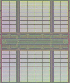
The new 64GB embedded device combines sixteen pieces of 32Gbit (equal to 4GB) NAND chips fabricated with Toshiba's cutting-edge 32nm process technology, and also integrates a dedicated controller. Toshiba is the first company to succeed in combining 16 pieces of 32Gbit NAND chips, and applied advanced chip thinning and layering technologies to realize individual chips that are only 30 micrometers thick. Full compliance with the JEDEC/MMCA Version 4.4(V4.4) standard for embedded MultiMediaCards supports standard interfacing and simplifies embedding in products, reducing development burdens on product manufacturers. Toshiba offers a comprehensive line-up of single-package embedded NAND Flash memories in densities ranging from 2GB to 64GB. All integrate a controller to manage basic control functions for NAND applications, and are compatible with the latest e-MMC standard and its new features, including defining multiple storage areas and enhanced security features.
The new 64GB embedded device combines sixteen pieces of 32Gbit (equal to 4GB) NAND chips fabricated with Toshiba's cutting-edge 32nm process technology, and also integrates a dedicated controller. Toshiba is the first company to succeed in combining 16 pieces of 32Gbit NAND chips, and applied advanced chip thinning and layering technologies to realize individual chips that are only 30 micrometers thick. Full compliance with the JEDEC/MMCA Version 4.4(V4.4) standard for embedded MultiMediaCards supports standard interfacing and simplifies embedding in products, reducing development burdens on product manufacturers. Toshiba offers a comprehensive line-up of single-package embedded NAND Flash memories in densities ranging from 2GB to 64GB. All integrate a controller to manage basic control functions for NAND applications, and are compatible with the latest e-MMC standard and its new features, including defining multiple storage areas and enhanced security features.