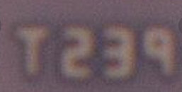
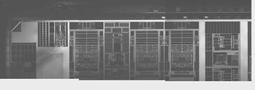
Nintendo Switch 2's Chipset Reportedly Confirmed as Tegra "T239" Unit
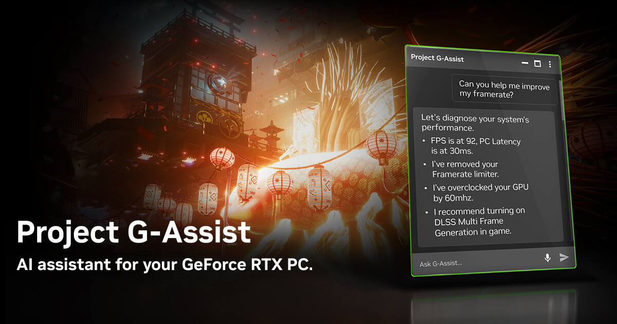
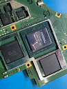
An alleged partial close-up capture of the Nintendo Switch 2's chipset has leaked out; courtesy of Kurnal (@Kurnalsalts). This fresh leak is being hyped up as putting an end to all online debate regarding the upcoming hybrid console's technological underpinnings. Despite late 2024/early 2025 reports pointing to a custom NVIDIA "T239" SoC design, certain voices continued to produce conjecture about a more "cutting edge" solution. Surprisingly, Team Green's PR department did issue a statement about the Switch 2 being powered by: "a custom processor featuring an NVIDIA GPU with dedicated RT Cores and Tensor Cores for stunning visuals and AI-driven enhancements."
As expected, Nintendo staffers remained guarded during recent press junkets—in-depth tech talk was deferred in NVIDIA's general direction. Kurnal's sharing of a speculative "T239" partial die shot does not provide any major new revelations or insights—as discussed on the Nintendo Switch 2 Subreddit, tech enthusiasts continue to rely on specification details from the big hack of NVIDIA repositories (three years ago). Newer speculation has focused on Nintendo's choice of foundry—Digital Foundry's Richard Leadbetter continues to express his personal belief that Nintendo has selected a Samsung 8 nm DUV foundry node. In opposition, certain critics have persisted with a 5 nm EUV node process theory.
As expected, Nintendo staffers remained guarded during recent press junkets—in-depth tech talk was deferred in NVIDIA's general direction. Kurnal's sharing of a speculative "T239" partial die shot does not provide any major new revelations or insights—as discussed on the Nintendo Switch 2 Subreddit, tech enthusiasts continue to rely on specification details from the big hack of NVIDIA repositories (three years ago). Newer speculation has focused on Nintendo's choice of foundry—Digital Foundry's Richard Leadbetter continues to express his personal belief that Nintendo has selected a Samsung 8 nm DUV foundry node. In opposition, certain critics have persisted with a 5 nm EUV node process theory.