"GFX1153" Target Spotted in AMDGPU Library Amendment, RDNA 3.5 Again Linked to "Medusa Point" APU
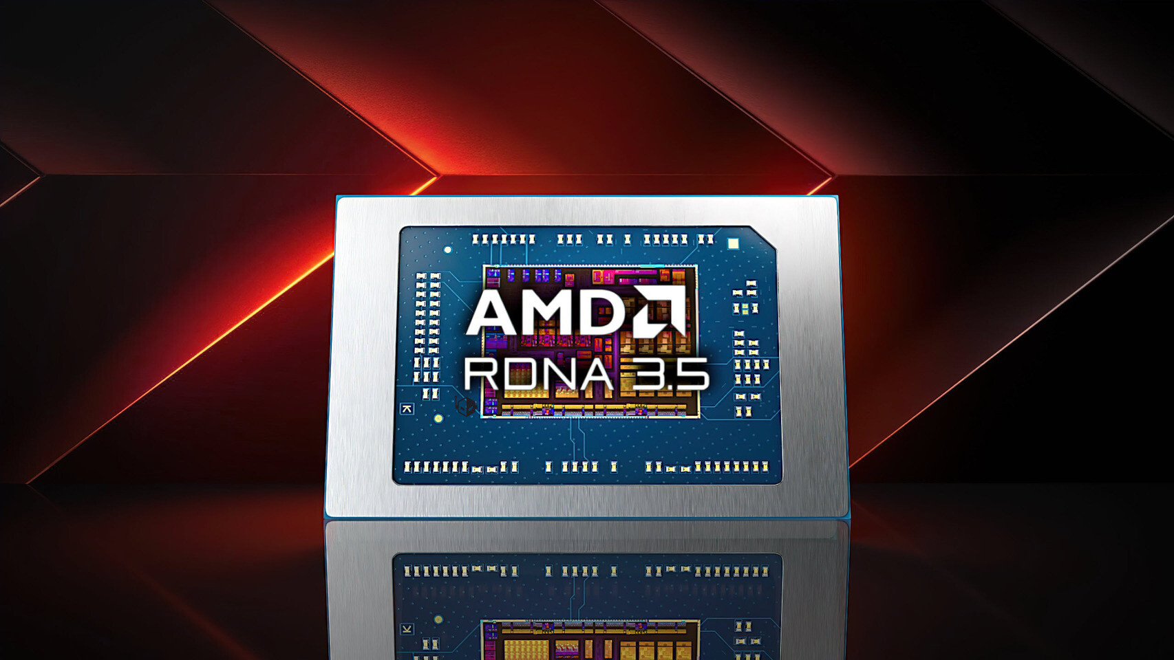
At the tail end of 2024, AMD technical staffers added the "GFX1153" target to their first-party GPU supported chip list. Almost three months later, PC hardware news outlets and online enthusiasts have just picked up on this development. "GFX1150" family IPs were previously linked to Team Red's RDNA 3.5 architecture. This graphics technology debuted with the launch of Ryzen AI "Strix Halo," "Strix Point" and "Krackan Point" mobile processors. Recent leaks have suggested that Team Red is satisfied with the performance of RDNA 3.5-based Radeon iGPUs; warranting a rumored repeat rollout with next-gen "Medusa Point" APU designs.
Both "Medusa Point" and "Gorgon Point" mobile CPU families are expected to launch next year, with leaks pointing to the utilization of "Zen 6" and "Zen 5" processor cores (respectively) and RDNA 3.5 graphics architecture. RDNA 4 seems to be a strictly desktop-oriented generation. AMD could be reserving the "further out" UDNA tech for truly next-generation integrated graphics solutions. In the interim, Team Red's "GFX1153" IP will likely serve as "Medusa Point's" onboard GPU, according to the latest logical theories. Last year, the "GFX1152" target was associated with Ryzen AI 7 300-series "Krackan Point" APUs.


Both "Medusa Point" and "Gorgon Point" mobile CPU families are expected to launch next year, with leaks pointing to the utilization of "Zen 6" and "Zen 5" processor cores (respectively) and RDNA 3.5 graphics architecture. RDNA 4 seems to be a strictly desktop-oriented generation. AMD could be reserving the "further out" UDNA tech for truly next-generation integrated graphics solutions. In the interim, Team Red's "GFX1153" IP will likely serve as "Medusa Point's" onboard GPU, according to the latest logical theories. Last year, the "GFX1152" target was associated with Ryzen AI 7 300-series "Krackan Point" APUs.