 163
163
AMD Radeon RX 5700 XT Review
(163 Comments) »Introduction
AMD today takes a swing at the lucrative performance segment of PC graphics with the Radeon RX 5700 series. This price band, ranging from $350 to $500, has graphics cards you'd want for serious gaming at resolutions of 1440p and above, or 1080p with high refresh rates. The lack of much serious competition from AMD for the past couple of years has given NVIDIA an unchallenged dominance with which it could sell the 6 GB GeForce RTX 2060 for as high as $400 on some partner models, and the RTX 2070 starting at $500, with some partner models even touching $600.
NVIDIA's generally high pricing for its RTX 20-series has been supported by the GPU's new real-time raytracing and AI acceleration capabilities, which do seem to take up billions of transistors on the silicon. NVIDIA was also the first adopter of the GDDR6 memory, which may have been pricey initially. AMD's official position on real-time raytracing for the client segment is that while it is one of the new innovations, it's not a killer feature that should influence your buying decisions. Today's 3D games are still rasterized and will be for the foreseeable future. You should hence base your buying on classic parameters, such as gaming performance, energy-efficiency, noise, future-proofing, and overclocking-headroom, or so believes AMD.

The AMD Radeon RX 5700 lineup consists of two models at this time: the RX 5700 XT and the RX 5700. Both cards are based on the swanky new "Navi 10" silicon built on the 7 nanometer silicon fabrication process at TSMC. This is AMD's second 7 nm GPU after "Vega 20." Unlike Vega, which used HBM2 memory, Navi is more purpose-built for the client segment and retains the conventional single-die package and external memory chips. This is AMD's first GPU to implement GDDR6, the new high-performance memory standard with a data rate as high as 14 Gbps, which translates to 448 GB/s of memory bandwidth across the 256-bit wide memory bus, which is similar to the bandwidth the "Vega 10" silicon achieved with 2048-bit HBM2 memory.
Navi also implements PCI-Express gen 4.0, a new bus standard that doubles host interface bandwidth over PCI-Express gen 3.0. AMD is also launching its "Valhalla" desktop platform today, which combines a 3rd generation Ryzen processor with a motherboard based on the AMD X570 chipset. This is the only platform with PCIe gen 4.0 support until Intel "Ice Lake" comes along. Of course, Navi Radeon RX 5700 fully supports older PCIe standards and should run at gen 3.0 or lower just fine. The blurbs "7 nm" and "PCIe gen 4.0" are extensively used in AMD's packaging of these products, as if to say that "Navi" is a generation ahead of the competition that's stuck with 12 nm and PCIe gen 3.
"Navi" isn't an optical shrink and upscaling of AMD's existing GPU IP to 7 nm (which is what "Vega 20" was). Instead, it introduces the first major update to the core number-crunching machinery of the GPU since 2013, when AMD introduced Graphics Core Next (GCN). In its place, AMD is debuting the new RDNA SIMD architecture, which has numerous innovations that increase IPC over GCN without losing the kind of parallelism that made GCN rock at general compute applications. On the following pages, we will dive deep into the nuts and bolts of RDNA.
AMD also used the opportunity to update its display engine, adding support for more display formats and 8K over a single cable due to DSC 1.2a, or 4K at higher refresh rates. Radeon RX 5700 also has updated multimedia hardware acceleration to support some of the newer consumer video formats, such as H.265 HEVC and VP9 at various 4K and 8K resolutions.
The Radeon RX 5700 XT we are examining in this review today leads the pack at $399, a whole $100 cheaper than the GeForce RTX 2070 and recently announced RTX 2070 Super. There is a slightly faster AMD 50th Anniversary Edition of this card at $449, but it is a very limited launch and won't be considered standard for this SKU. The RX 5700 XT maxes out the 7 nm "Navi 10" silicon featuring 2,560 stream processors, 160 TMUs, and 64 ROPs. That's right, AMD has finally broadened its render-backends to improve raster performance. Until now, only the larger Vega GPUs and their high-end predecessors had such a high ROP count. NVIDIA implemented 64 ROPs on its performance-segment GPUs since "Maxwell". The RX 5700 we are reviewing in a second review today is a slightly cut down sibling that's $50 cheaper at $349.
Our exhaustive coverage of AMD's 7/7 Launch Day includes the following content:
AMD Ryzen 9 3900X 12-core processor | AMD Ryzen 7 3700X 8-core processor | AMD Radeon RX 5700 XT graphics card | AMD Radeon RX 5700 graphics card | AMD Zen 2 Memory Performance Scaling | Ryzen 3900X and 3700 on X470 vs X570 platforms | Radeon RX 5700 XT Navi PCI-Express 4.0 Performance Scaling | ASRock X570 Taichi motherboard | ASUS Prime X570-Pro motherboard
| Price | Shader Units | ROPs | Core Clock | Boost Clock | Memory Clock | GPU | Transistors | Memory | |
|---|---|---|---|---|---|---|---|---|---|
| RX Vega 56 | $300 | 3584 | 64 | 1156 MHz | 1471 MHz | 800 MHz | Vega 10 | 12500M | 8 GB, HBM2, 2048-bit |
| GTX 1660 Ti | $280 | 1536 | 48 | 1500 MHz | 1770 MHz | 1500 MHz | TU116 | 6600M | 6 GB, GDDR6, 192-bit |
| GTX 1070 Ti | $450 | 2432 | 64 | 1607 MHz | 1683 MHz | 2000 MHz | GP104 | 7200M | 8 GB, GDDR5, 256-bit |
| RTX 2060 | $340 | 1920 | 48 | 1365 MHz | 1680 MHz | 1750 MHz | TU106 | 10800M | 6 GB, GDDR6, 192-bit |
| RX 5700 | $350 | 2304 | 64 | 1465 MHz | 1625 MHz | 1750 MHz | Navi 10 | 10300M | 8 GB, GDDR6, 256-bit |
| GTX 1080 | $500 | 2560 | 64 | 1607 MHz | 1733 MHz | 1251 MHz | GP104 | 7200M | 8 GB, GDDR5X, 256-bit |
| RTX 2060 Super | $400 | 2176 | 64 | 1470 MHz | 1650 MHz | 1750 MHz | TU106 | 10800M | 8 GB, GDDR6, 256-bit |
| RX Vega 64 | $500 | 4096 | 64 | 1247 MHz | 1546 MHz | 953 MHz | Vega 10 | 12500M | 8 GB, HBM2, 2048-bit |
| GTX 1080 Ti | $700 | 3584 | 88 | 1481 MHz | 1582 MHz | 1376 MHz | GP102 | 12000M | 11 GB, GDDR5X, 352-bit |
| RX 5700 XT | $400 | 2560 | 64 | 1605 MHz | 1755 MHz | 1750 MHz | Navi 10 | 10300M | 8 GB, GDDR6, 256-bit |
| RTX 2070 | $480 | 2304 | 64 | 1410 MHz | 1620 MHz | 1750 MHz | TU106 | 10800M | 8 GB, GDDR6, 256-bit |
| RTX 2070 Super | $500 | 2560 | 64 | 1605 MHz | 1770 MHz | 1750 MHz | TU104 | 13600M | 8 GB, GDDR6, 256-bit |
| Radeon VII | $680 | 3840 | 64 | 1802 MHz | N/A | 1000 MHz | Vega 20 | 13230M | 16 GB, HBM2, 4096-bit |
| RTX 2080 | $700 | 2944 | 64 | 1515 MHz | 1710 MHz | 1750 MHz | TU104 | 13600M | 8 GB, GDDR6, 256-bit |
| RTX 2080 Super | $700 | 3072 | 64 | 1650 MHz | 1815 MHz | 1940 MHz | TU104 | 13600M | 8 GB, GDDR6, 256-bit |
| RTX 2080 Ti | $1100 | 4352 | 64 | 1350 MHz | 1545 MHz | 1750 MHz | TU102 | 18600M | 11 GB, GDDR6, 352-bit |
Architecture: Navi and RDNA


We've been hearing the moniker "Navi" for years now, and AMD threw another one at us this Computex, "RDNA", so let us demystify the two first. "Navi" is the codename for the family of silicon the GPU is based on. RDNA is a new architecture introduced by AMD to succeed Graphics Core Next (GCN). It prescribes the GPU's component hierarchy and, more importantly, its main number-crunching machinery, the compute units.
Another example of this distinction would be "Vega". Vega 10, Vega 20, and Vega 12 are pieces of silicon from the same family, while the GPU follows the 5th generation Graphics Core Next architecture governing even its compute units. Over many years, AMD made incremental updates to GCN, but this time, it claims that RDNA is sufficiently different from GCN to not be considered a new version, but rather a new hardware component that brings with it massive IPC gains over the previous generation.


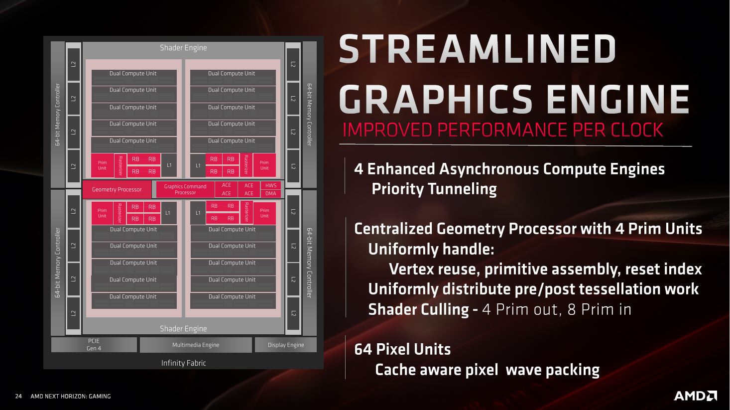
The Radeon RX 5700 series is built around "Navi 10," an elegant little piece of silicon engineered on the 7 nm process at TSMC, with 10.3 billion transistors crammed into a die measuring just 251 mm². The chip features a PCI-Express 4.0 x16 bus interface and a 256-bit wide GDDR6 memory interface. Infinity Fabric, which debuted on AMD's Ryzen CPUs, is extensively used as an on-die interconnect linking the various major components.
The bulk of AMD's engineering effort with RDNA has been to increase the number of dedicated resources to avoid starvation by fewer components waiting for access to a resource. The "Navi 10" silicon has two Shader Engines sharing a centralized Command Processor that distributes workloads, a Geometry Processor, and ACEs (asynchronous compute engines).


Each Shader Engine is further divided into two Graphics Engines. A graphics engine shares render backends, a Rasterizer, and a Prim Unit among five Workgroup Processors. This is where the core of RDNA begins. AMD figured it could merge two compute units (CUs) to share schedulers, scalar units, a data-share, instruction and data caches, and TMUs. The Workgroup Processor, or "dual-compute unit" as shown in the architecture block diagram, is for all intents and purposes indivisible, in that individual CUs cannot be disabled.

An RDNA compute unit packs 64 stream processors for vector operations and double the number of scalar units for localized serial processing. The stream processors in a CU are split into groups of two, each equipped with a scalar unit. According to AMD, this greatly reduces latency and improves the overall IPC of the compute unit. It also more efficiently utilizes local caches.

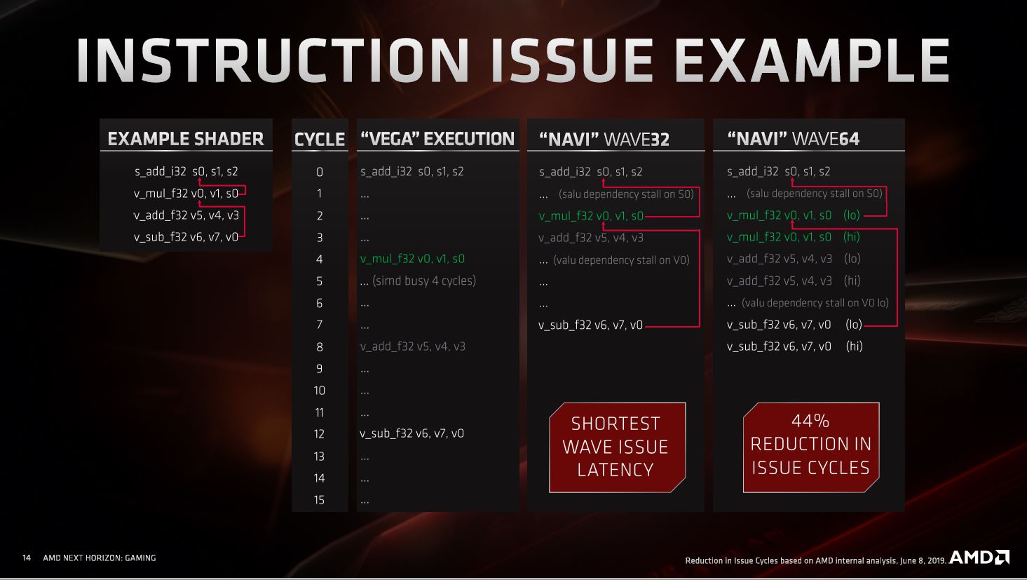
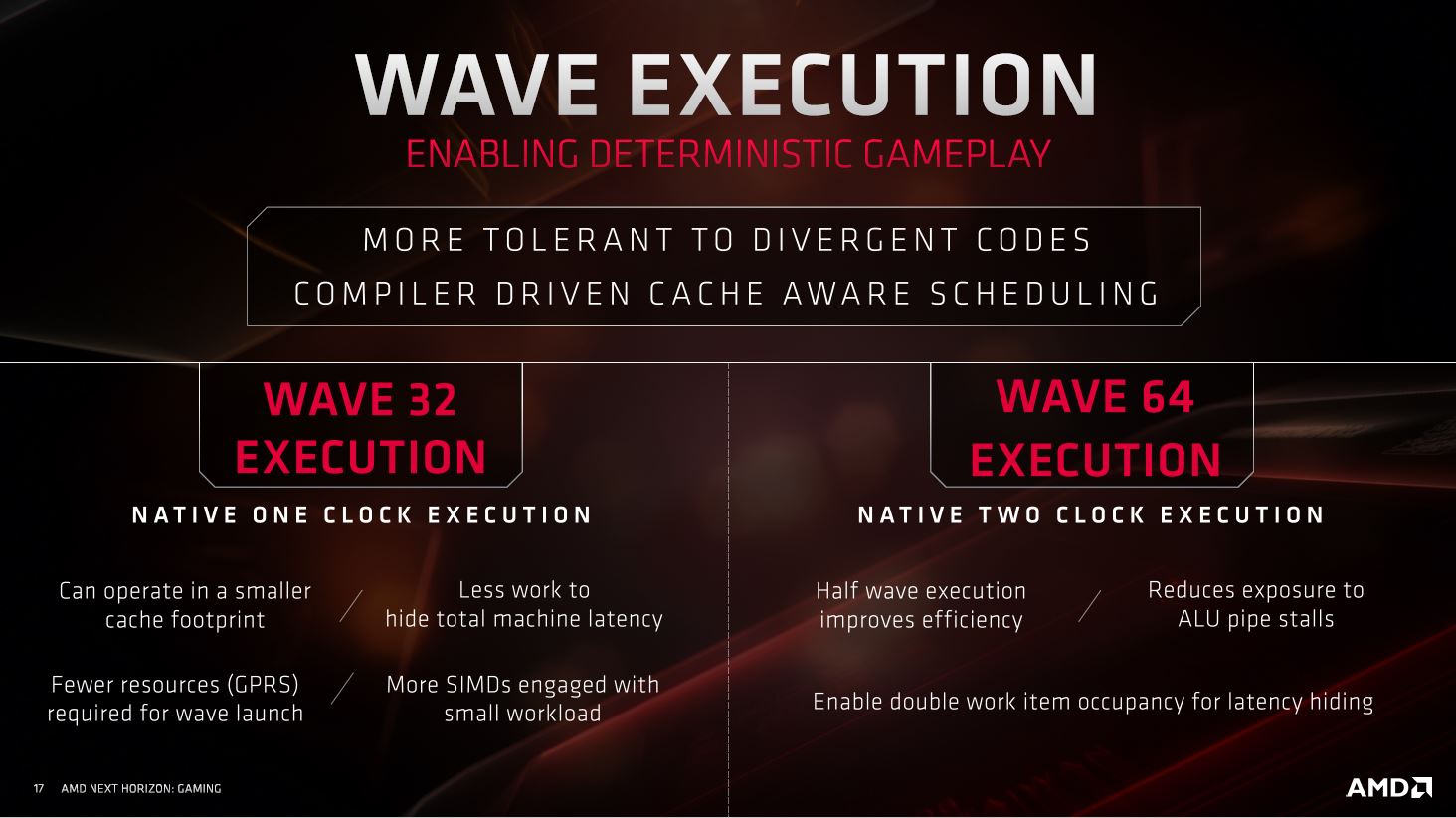
The vector execution units, or stream processors, is where much of the GPU's parallel processing happens. Due to the redesigned compute unit, two scalar processors pull two SIMD32 vector units made up of 32 stream processors, each, instead of a single scalar processor pulling four SIMD16 vector units. How is this important? On GCN, the way SIMD units are laid out, all items in a Wave64 operation get to do work once every four clocks due to hardware interleaving. With RDNA, Wave32 work items can do work every clock cycle. In all, RDNA minimizes wasted clock cycles by more efficiently and uniformly utilizing the hardware resources.

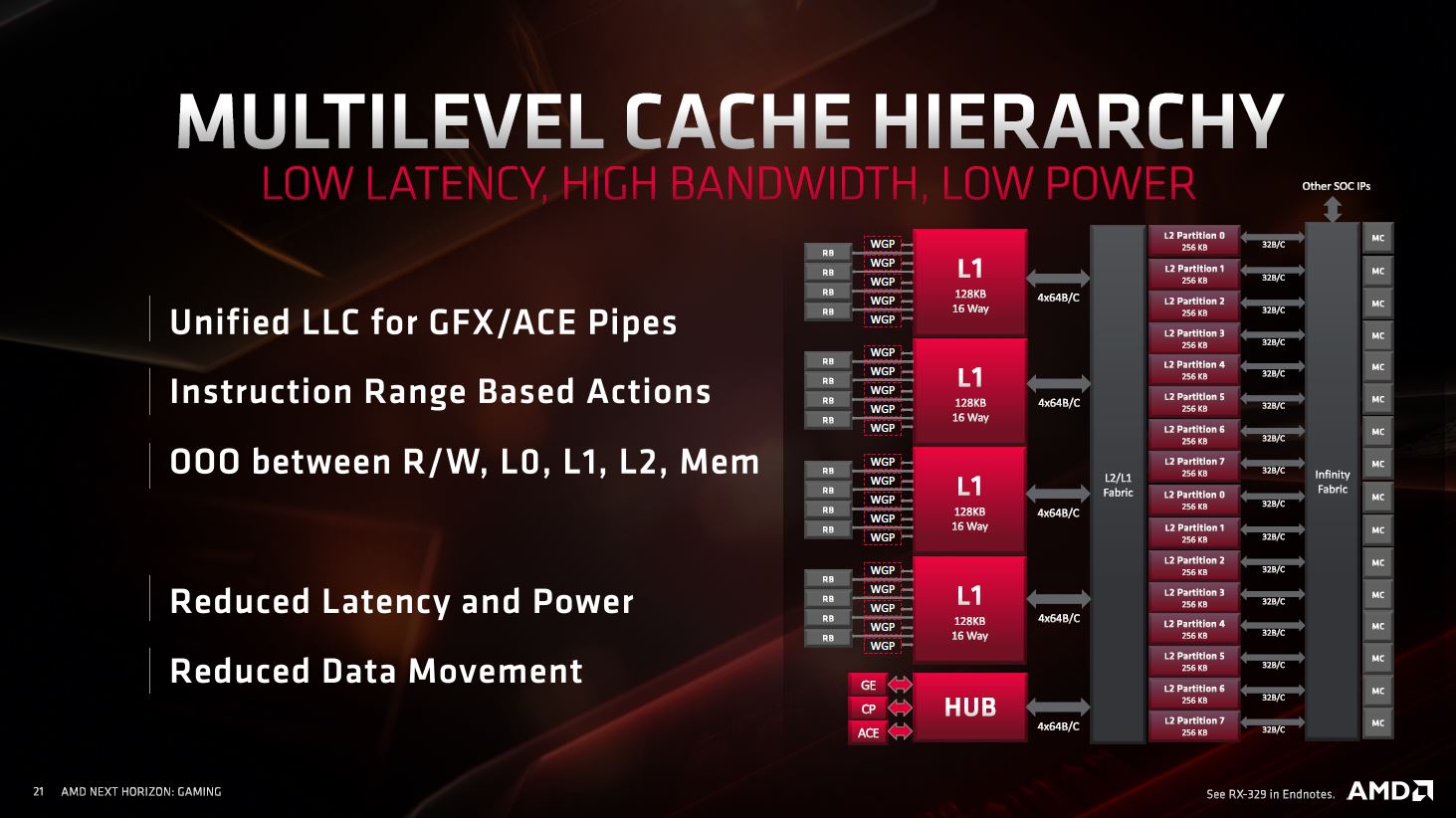
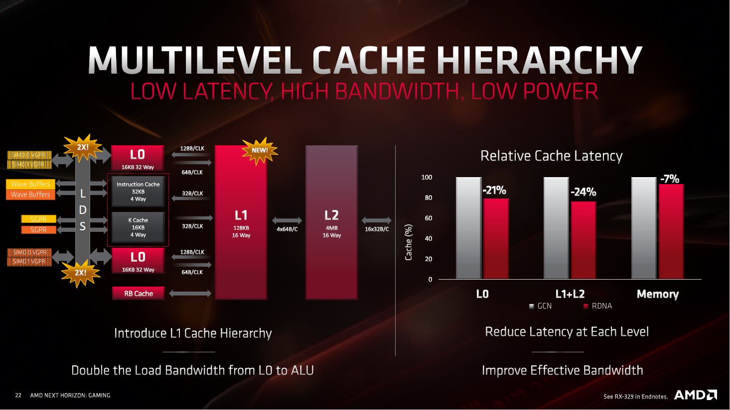
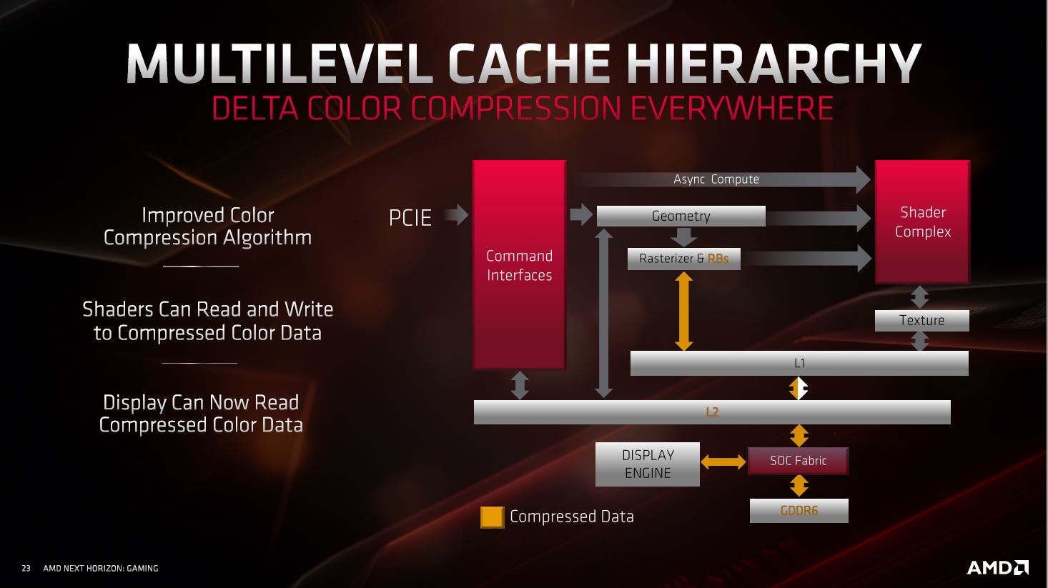
AMD examined previous generations of its graphics architecture to locate bottlenecks in the graphics pipeline. Besides increasing the number of dedicated resources, the company reworked the chip's cache hierarchy by cushioning data transfers at various stages. Each workgroup processor has dedicated 32 KB instruction and 16 KB data caches, which write back to a 128 KB L1 cache dedicated to each Graphics Engine.
These L1 caches talk to 4 MB of L2 cache. The introduction of the L1 cache and doubling in bandwidth between the various caches contributes greatly to IPC as it minimizes memory accesses, which are much slower than cache accesses. AMD is also using faster (lower latency) SRAM that reduces cache latencies by around 20 percent on die and by 8 percent at the memory level. AMD also introduced new features to the ACEs that include async-compute tunneling.

AMD summarizes the benefits of RDNA in a 25 percent IPC gain over the latest version of GCN, and an effective 50 percent performance gain for the GPU when taking into account IPC, the 7 nm process, and gains from the frequency and power management (ability to sustain boost frequencies better).


Elsewhere on the silicon, AMD updated the Display Engine and Multimedia Engine to keep up with the latest display and video standards. The Display Engine now supports DSC 1.2a (display stream compression) along with output standards HDMI 2.0 and DisplayPort 1.4 HDR to support display formats as bandwidth-intensive as 4K 240 Hz or 8K 60 Hz over a single cable, and support for 30 bits per pixel color depth. The multimedia engine supports VP9 and H.265 decoding at up to 8K 24 Hz, or 4K 90 Hz, and hardware-accelerated H.265 encoding at up to 4K 60 Hz.
Features: FidelityFX and Anti-Lag


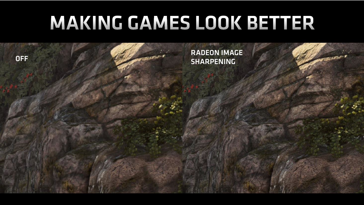
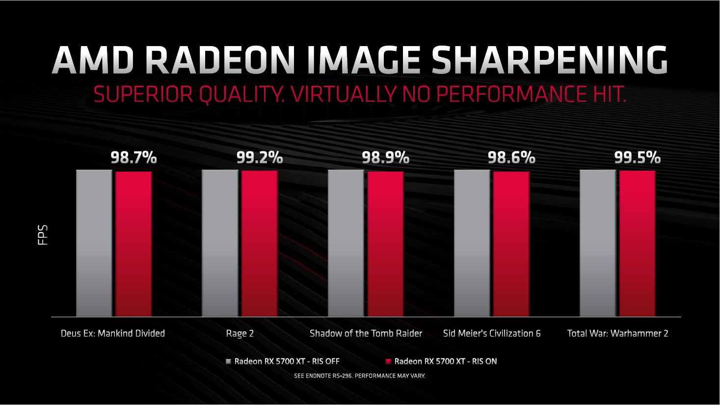
With each new graphics architecture, gamers expect new image quality enhancement features. NVIDIA introduced DLSS, and AMD's response to that is FidelityFX, a combination of content-specific and image-specific quality enhancements. The first part of this is contrast-adaptive sharpening, which brings out details in a scene by enhancing their contrast. To work best, it requires some work from game developers, to declare which parts of the image are to be sharpened (like the HUD and on-screen texts). Details such as wear-lines on the slick tires of a race-car,or hexagonal patterns on a wall come to life. We will test this feature later in a separate article.


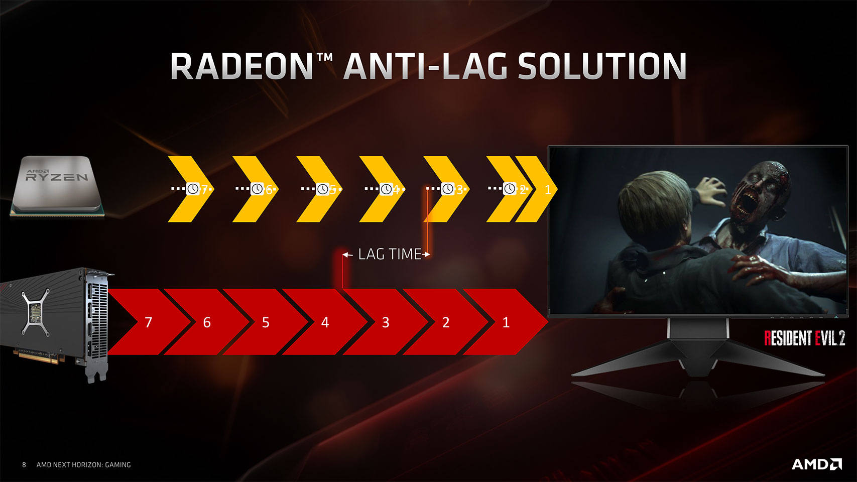
AMD wants to improve its adoption by professional e-Sports gamers by addressing a key bottleneck with modern high-end graphics: mouse-lag. This would be the amount of time taken for a click to register and a response to be rendered by the GPU. Radeon Anti-Lag is a CTR (click-to-response) enhancement that reduced mouse lag by roughly a third across various popular e-Sports titles. This setting is effectively identical to "pre-rendered" frames on NVIDIA. Modern GPUs calculate one or two frames ahead, so they can better time sending them to the monitor to avoid stuttering. Of course, this results in input lag because any input information that comes in only makes it to the screen one or two frames later.
Packaging and Contents


You will receive:
- Graphics card
- Documentation
The Card


At first glance, the card looks similar to Vega reference designs, which isn't surprising because AMD kept their "blocky" design language with clear edges and is using the exact same form factor: 27.0 x 11.0 cm. Instead of a smooth surface, the metal shroud has little horizontal ridges that significantly improve the look and give it a really nice feel when holding the card in your hands. A high-quality metal backplate is included with the card.

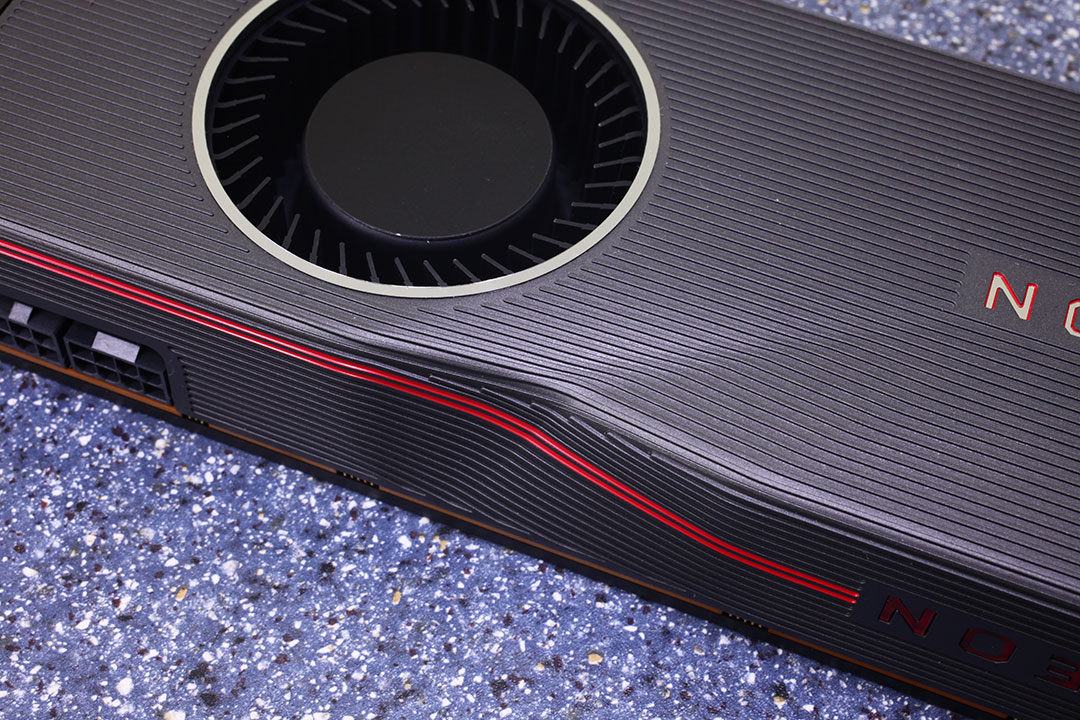
When taking a closer look, a bend in the cooler quickly draws attention. According to AMD, it was not only added for aesthetic reasons as it also improves performance of the blower cooler.

Installation requires two slots in your system.

Display connectivity options include three standard DisplayPort 1.4a and an HDMI 2.0b.
AMD took the opportunity to update the display controllers handling these outputs by leveraging DSC 1.2a (display stream compression), which unlocks very high resolution and refresh-rate combinations over a single cable. Among the single-cable display modes supported are 8K 60 Hz (which took two DP 1.3 cables until now), 4K 240 Hz, and 1080p as high as 360 Hz. On top of these, the outputs support HDR and 30 bpc color-depth for better color accuracy in creative applications.

The board uses an 8-pin and a 6-pin power connector. This input configuration is specified for up to 300 watts of power draw.

AMD's Navi generation of GPUs no longer supports CrossFire. DirectX 12 does include its own set of multi-GPU capabilities, but implementation requires game developers to put serious development time into a feature only a tiny fraction of their customers might ever use.
Our Patreon Silver Supporters can read articles in single-page format.
Apr 24th, 2025 00:16 EDT
change timezone
Latest GPU Drivers
New Forum Posts
- Which is the best replacement for Microsoft Office? (23)
- RX 9000 series GPU Owners Club (500)
- Asus Rx570 o4g cannot losd drivers error code 43 (13)
- How do you calculate the cost of a chip? (4)
- need help with 12900hx (6)
- Are the 8 GB cards worth it? (108)
- 5060 Ti 8GB DOA (257)
- Help getting a mini pc (7)
- 5070ti overclock...what are your settings? (16)
- New GPU 5070 Ti or better CPU Ryzen7 7800X3D ? (6)
Popular Reviews
- NVIDIA GeForce RTX 5060 Ti 8 GB Review - So Many Compromises
- ASUS GeForce RTX 5060 Ti TUF OC 16 GB Review
- ASRock X870E Taichi Lite Review
- Colorful iGame B860M Ultra V20 Review
- Upcoming Hardware Launches 2025 (Updated Apr 2025)
- Sapphire Radeon RX 9070 XT Pulse Review
- Sapphire Radeon RX 9070 XT Nitro+ Review - Beating NVIDIA
- NVIDIA GeForce RTX 5060 Ti PCI-Express x8 Scaling
- AMD Ryzen 7 9800X3D Review - The Best Gaming Processor
- ASUS GeForce RTX 5080 TUF OC Review
Controversial News Posts
- NVIDIA GeForce RTX 5060 Ti 16 GB SKU Likely Launching at $499, According to Supply Chain Leak (182)
- NVIDIA Sends MSRP Numbers to Partners: GeForce RTX 5060 Ti 8 GB at $379, RTX 5060 Ti 16 GB at $429 (127)
- NVIDIA Launches GeForce RTX 5060 Series, Beginning with RTX 5060 Ti This Week (115)
- Nintendo Confirms That Switch 2 Joy-Cons Will Not Utilize Hall Effect Stick Technology (105)
- Nintendo Switch 2 Launches June 5 at $449.99 with New Hardware and Games (99)
- Sony Increases the PS5 Pricing in EMEA and ANZ by Around 25 Percent (85)
- NVIDIA PhysX and Flow Made Fully Open-Source (77)
- Windows Notepad Gets Microsoft Copilot Integration (75)