 474
474
AMD Ryzen 7 9800X3D Review - The Best Gaming Processor
(474 Comments) »Introduction
The new AMD Ryzen 7 9800X3D is an unexpected entry to the 2024 processor product launch cycle—gamers will be happy. AMD's X3D processor lineup features 3D vertical-stacked cache, or 3D V-Cache. AMD designed the CPU complex dies (CCDs) of recent Ryzen CPUs in a way that the 32 MB on-die L3 cache can be expanded to 96 MB with stacked cache dies. This large cache is known to have a profound impact on gaming performance. With the X3D processors, AMD is going for gaming performance leadership. It knows the enthusiast PC segment as well as Intel does, and how big a role gaming performance plays in processor and platform selection. This is why the company innovated the X3D series.
The Ryzen 7 9800X3D comes in just three months after the company's debut of the Ryzen 9000 series processors powered by the latest Zen 5 microarchitecture. It is widely believed that the November 2024 launch of the 9800X3D was deliberate, so the chip could clash with Intel Core Ultra Series 200 family powered by the Arrow Lake microarchitecture. Before we could get our hands on the latest Intel chips, we had honestly expected Arrow Lake to deliver a significant gaming performance improvement over Raptor Lake, and we're sure AMD did the same. Not wanting to end up with a situation where processors such as the 7800X3D are wildly outclassed by Intel, the company probably rushed in the 9800X3D, the 8-core, single-CCD chip with the best chance at having the highest generational gaming performance leap.

Alas, interesting things happened over the past three months. The Zen 5 microarchitecture barely posted a 5% gaming performance increase over Zen 4, and worse, Arrow Lake barely beat Raptor Lake in gaming, in many cases ending up slower, albeit with an energy efficiency leap. Even the fastest Core Ultra 9 285K could not trump the Ryzen 7 7800X3D in gaming, and so the 9800X3D has a rather easy task ahead—simply to beat the 7800X3D, and extend AMD's gaming performance leadership over Intel.
Likely anticipating Arrow Lake to be much faster at gaming than it ended up being, AMD gave the 9800X3D two key improvements over the 7800X3D. Firstly, the company increased clock speeds. The 9800X3D ticks at a base frequency of 4.70 GHz, which is a 500 MHz increase over that of the 7800X3D. The maximum boost frequency is 200 MHz higher, at 5.20 GHz. This increase in base frequency means that the average clock frequencies over multiple cores will end up higher, even if the new Zen 5 microarchitecture doesn't have a significant contribution to gaming performance from its generational IPC increase, these clock speeds should see the 9800X3D through.
The second, and perhaps bigger innovation, is at a physical level—AMD inverted the CCD+L3D stack. In the past two generations of X3D desktop processors, namely the 7800X3D Raphael-X powered by Zen 4 and the 5800X3D Vermeer-X powered by Zen 3, the 3D V-Cache die is stacked on top of the CPU complex die (CCD). The chip would stack over the central region of the CCD that has the 32 MB on-die L3 cache, while structural silicon would top the peripheral regions of the CCD that had the CPU cores. This structural silicon levels out the stack, and handles the crucial task of transferring heat from the CPU cores to the surface, where it's picked up by the solder TIM, and transferred to the integrated heat spreader (IHS). With the new 9800X3D Granite Ridge-X, AMD has inverted the CCD+L3D stack. The CCD is now on top, and the L3D is below it. The L3D now has not just the 64 MB add-on L3 cache memory, but also serves as a sort of base tile for the CCD on top. It is peppered with TSVs in the peripheral region, so it could connect the Zen 5 CPU cores from the CCD to the fiberglass substrate below.
This inversion of the 3D V-Cache stack has the obvious advantage of the CCD's thermals behaving like they do on the regular Ryzen 9000 series processors without 3D V-Cache. There should be a marked improvement in heat transfer from the CPU cores to the STIM and IHS, which is how AMD was able to increase the base frequency significantly. Then there's also how Zen 5 X3D is said to now have the same overclocking capabilities as the regular 9000-series processors.
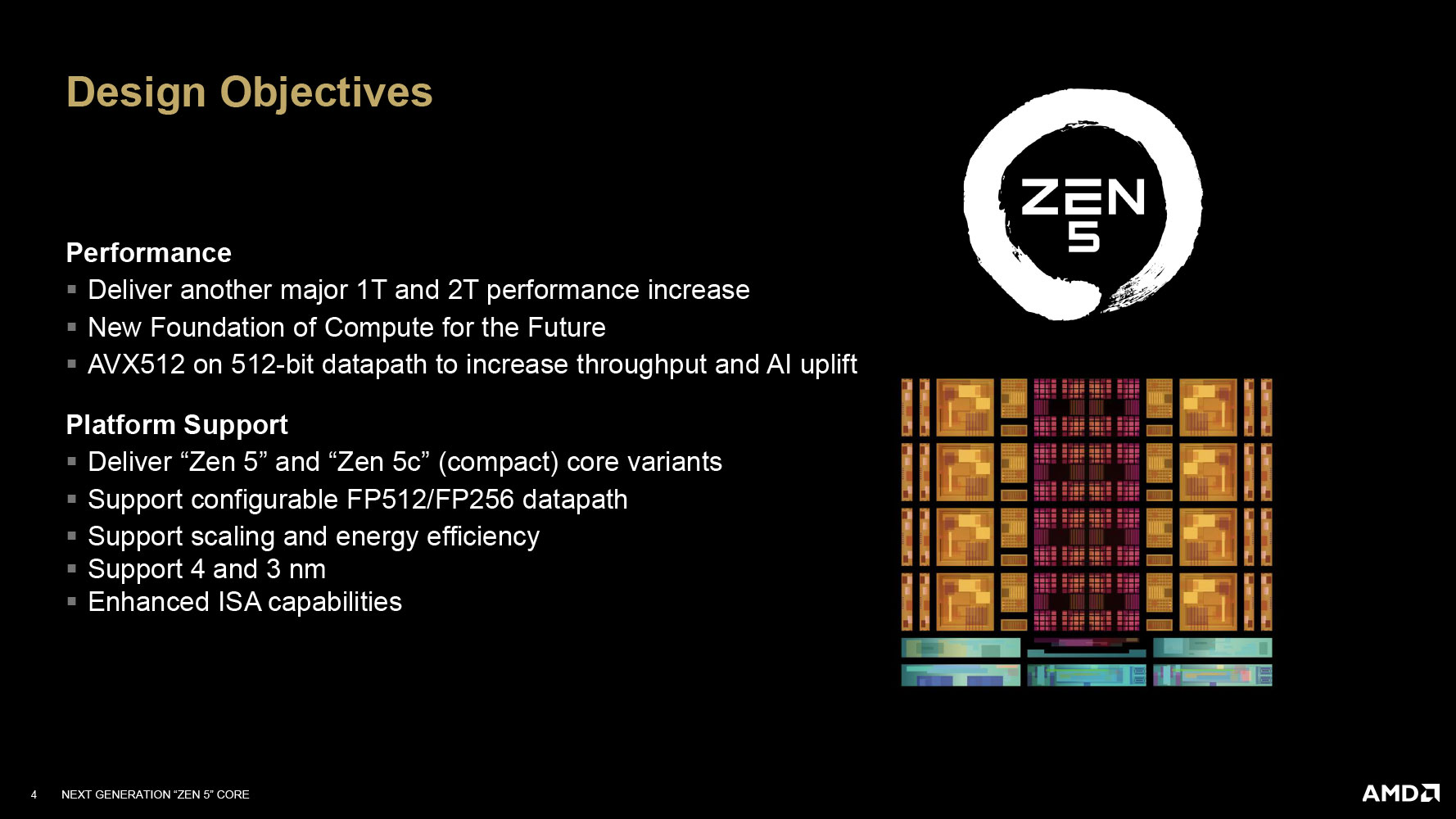
The new AMD Zen 5 microarchitecture sees the company rework pretty much all key components of the core compared to Zen 4, with a focus particularly on the number crunching machinery. The core comes with a true 512-bit floating point data-path to more effectively execute 512-bit SIMD workloads that use instruction-sets such as AVX-512, VNNI, etc.; when compared to Zen 4, which uses a dual-pumped 256-bit data-path to execute these instruction-sets. AMD also increased the bandwidth and associativity of the per core caches, and improved the bandwidth of the L3 cache. There are also generational improvements to the branch prediction unit. The CCD is built on the newer TSMC N4P (4 nm) foundry node, which improves power and clock speeds. Besides the 4.70 GHz base frequency and 5.20 GHz boost frequency, the Ryzen 7 9800X3D comes with a TDP of 120 W, same as that of the 7800X3D.
AMD is pricing the eight-core Ryzen 7 9800X3D at an eye-watering $480, a $30 increase over the launch price of the 7800X3D. It's also roughly $80 higher than the 20-core Core Ultra 7 265K and Core i7-14700K, while being just $40 cheaper than the Core i9-14900K and $80 less than the 285K. This is, in the end, an 8-core/16-thread processor. Apparently eight cores is all that games need, even Intel thinks so, which is why the company's P-core count tops out at eight. So, as an 8-core chip, the 9800X3D is being targeted squarely at gamers.
| Price | Cores / Threads | Base Clock | Max. Boost | L3 Cache | TDP | Architecture | Process | Socket | |
|---|---|---|---|---|---|---|---|---|---|
| Intel Core i5 | |||||||||
| Core i5-12400F | $110 | 6 / 12 | 2.5 GHz | 4.4 GHz | 18 MB | 65 W | Alder Lake | 10 nm | LGA 1700 |
| Core i5-13400F | $170 | 6+4 / 16 | 2.5 / 1.8 GHz | 4.6 / 3.3 GHz | 20 MB | 65 W | Raptor Lake | 10 nm | LGA 1700 |
| Core i5-12600K | $170 | 6+4 / 16 | 3.7 / 2.8 GHz | 4.9 / 3.6 GHz | 20 MB | 125 W | Alder Lake | 10 nm | LGA 1700 |
| Core i5-13600K | $225 | 6+8 / 20 | 3.5 / 2.6 GHz | 5.1 / 3.9 GHz | 24 MB | 125 W | Raptor Lake | 10 nm | LGA 1700 |
| Core i5-14600K | $260 | 6+8 / 20 | 3.5 / 2.6 GHz | 5.3 / 4.0 GHz | 24 MB | 125 W | Raptor Lake | 10 nm | LGA 1700 |
| Intel Core Ultra 5 | |||||||||
| Core Ultra 5 245K | $310 | 6+8 / 14 | 4.2 / 3.6 GHz | 5.2 / 4.6 GHz | 24 MB | 159 W | Arrow Lake | 3 nm | LGA 1851 |
| AMD Ryzen 5 | |||||||||
| Ryzen 5 8500G | $150 | 6 / 12 | 3.5 GHz | 5.0 GHz | 16 MB | 65 W | Phoenix 2 | 4 nm | AM5 |
| Ryzen 5 5600X | $135 | 6 / 12 | 3.7 GHz | 4.6 GHz | 32 MB | 65 W | Zen 3 | 7 nm | AM4 |
| Ryzen 5 7600 | $185 | 6 / 12 | 3.8 GHz | 5.1 GHz | 32 MB | 65 W | Zen 4 | 5 nm | AM5 |
| Ryzen 5 7600X | $210 | 6 / 12 | 4.7 GHz | 5.3 GHz | 32 MB | 105 W | Zen 4 | 5 nm | AM5 |
| Ryzen 5 9600X | $250 | 6 / 12 | 3.9 GHz | 5.4 GHz | 32 MB | 65 W | Zen 5 | 4 nm | AM5 |
| Intel Core i7 | |||||||||
| Core i7-12700K | $210 | 8+4 / 20 | 3.6 / 2.7 GHz | 5.0 / 3.8 GHz | 25 MB | 125 W | Alder Lake | 10 nm | LGA 1700 |
| Core i7-13700K | $280 | 8+8 / 24 | 3.4 / 2.5 GHz | 5.4 / 4.2 GHz | 30 MB | 125 W | Raptor Lake | 10 nm | LGA 1700 |
| Core i7-14700K | $355 | 8+12 / 28 | 3.4 / 2.5 GHz | 5.6 / 4.3 GHz | 33 MB | 125 W | Raptor Lake | 10 nm | LGA 1700 |
| Intel Core Ultra 7 | |||||||||
| Core Ultra 7 265K | $395 | 8+12 / 20 | 3.9 / 3.3 GHz | 5.5 / 4.6 GHz | 30 MB | 250 W | Arrow Lake | 3 nm | LGA 1851 |
| AMD Ryzen 7 | |||||||||
| Ryzen 7 5700G | $165 | 8 / 16 | 3.8 GHz | 4.6 GHz | 16 MB | 65 W | Zen 3 + Vega | 7 nm | AM4 |
| Ryzen 7 5700X | $160 | 8 / 16 | 3.4 GHz | 4.6 GHz | 32 MB | 65 W | Zen 3 | 7 nm | AM4 |
| Ryzen 7 7700 | $280 | 8 / 16 | 3.8 GHz | 5.3 GHz | 32 MB | 65 W | Zen 4 | 5 nm | AM5 |
| Ryzen 7 7700X | $275 | 8 / 16 | 4.5 GHz | 5.4 GHz | 32 MB | 105 W | Zen 4 | 5 nm | AM5 |
| Ryzen 7 9700X | $330 | 8 / 16 | 3.8 GHz | 5.5 GHz | 32 MB | 65 W | Zen 5 | 4 nm | AM5 |
| Ryzen 7 5800X | $165 | 8 / 16 | 3.8 GHz | 4.7 GHz | 32 MB | 105 W | Zen 3 | 7 nm | AM4 |
| Ryzen 7 5800X3D | $340 | 8 / 16 | 3.4 GHz | 4.5 GHz | 96 MB | 105 W | Zen 3 | 7 nm | AM4 |
| Ryzen 7 7800X3D | $450 | 8 / 16 | 4.2 GHz | 5.0 GHz | 96 MB | 120 W | Zen 4 | 5 nm | AM5 |
| Ryzen 7 9800X3D | $480 | 8 / 16 | 4.7 GHz | 5.2 GHz | 96 MB | 120 W | Zen 5 | 4 nm | AM5 |
| Intel Core i9 | |||||||||
| Core i9-12900K | $280 | 8+8 / 24 | 3.2 / 2.4 GHz | 5.2 / 3.9 GHz | 30 MB | 125 W | Alder Lake | 10 nm | LGA 1700 |
| Core i9-13900K | $415 | 8+16 / 32 | 3.0 / 2.2 GHz | 5.8 / 4.3 GHz | 36 MB | 125 W | Raptor Lake | 10 nm | LGA 1700 |
| Core i9-14900K | $445 | 8+16 / 32 | 3.2 / 2.4 GHz | 6.0 / 4.4 GHz | 36 MB | 125 W | Raptor Lake | 10 nm | LGA 1700 |
| Intel Core Ultra 9 | |||||||||
| Core Ultra 9 285K | $590 | 8+16 / 24 | 3.7 / 3.2 GHz | 5.7 / 4.6 GHz | 36 MB | 250 W | Arrow Lake | 3 nm | LGA 1851 |
| AMD Ryzen 9 | |||||||||
| Ryzen 9 5900X | $265 | 12 / 24 | 3.7 GHz | 4.8 GHz | 64 MB | 105 W | Zen 3 | 7 nm | AM4 |
| Ryzen 9 7900 | $370 | 12 / 24 | 3.7 GHz | 5.4 GHz | 64 MB | 65 W | Zen 4 | 5 nm | AM5 |
| Ryzen 9 7900X | $400 | 12 / 24 | 4.7 GHz | 5.6 GHz | 64 MB | 170 W | Zen 4 | 5 nm | AM5 |
| Ryzen 9 7900X3D | $580 | 12 / 24 | 4.4 GHz | 5.6 GHz | 128 MB | 120 W | Zen 4 | 5 nm | AM5 |
| Ryzen 9 9900X | $430 | 12 / 24 | 4.4 GHz | 5.6 GHz | 64 MB | 120 W | Zen 5 | 4 nm | AM5 |
| Ryzen 9 5950X | $345 | 16 / 32 | 3.4 GHz | 4.9 GHz | 64 MB | 105 W | Zen 3 | 7 nm | AM4 |
| Ryzen 9 7950X | $510 | 16 / 32 | 4.5 GHz | 5.7 GHz | 64 MB | 170 W | Zen 4 | 5 nm | AM5 |
| Ryzen 9 7950X3D | $550 | 16 / 32 | 4.2 GHz | 5.7 GHz | 128 MB | 120 W | Zen 4 | 5 nm | AM5 |
| Ryzen 9 9950X | $600 | 16 / 32 | 4.3 GHz | 5.7 GHz | 64 MB | 170 W | Zen 5 | 4 nm | AM5 |
Architecture
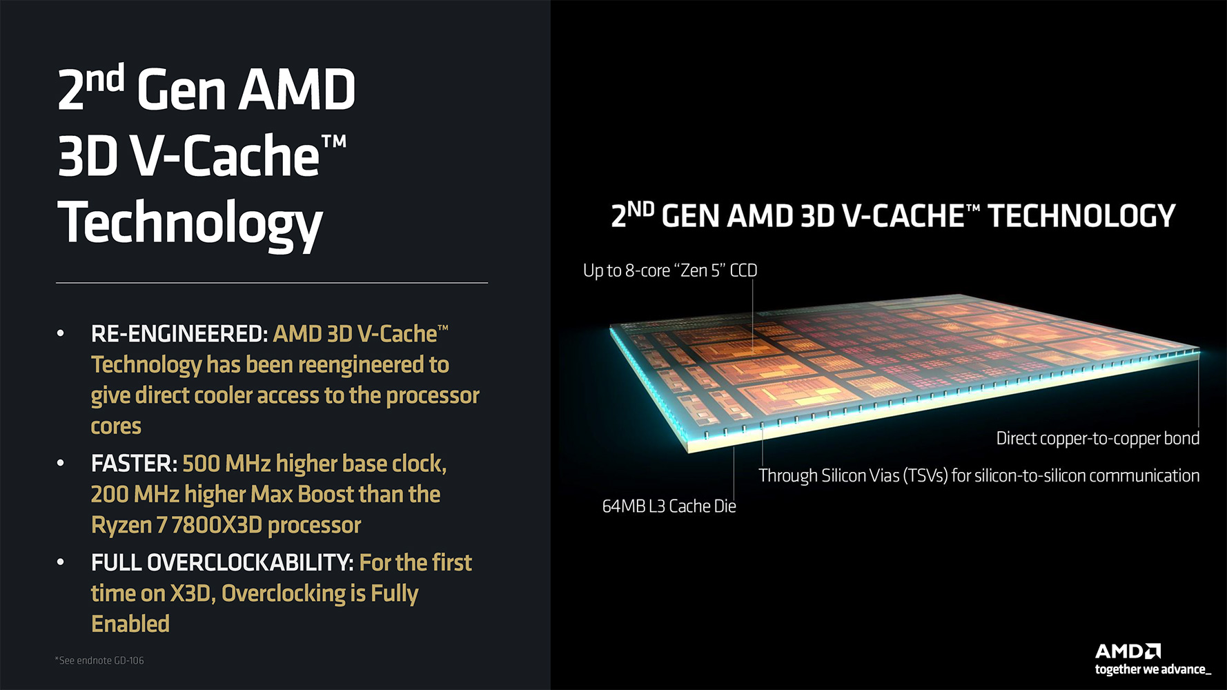
The Ryzen 7 9800X3D is the first processor from the 9000X3D family of desktop processors that combine the new Zen 5 microarchitecture with 3D V-Cache technology. AMD plans to launch other chips from the family in early 2025. The 9000X3D series debuts the second generation of 3D V-Cache technology. In past generations of X3D chips, such as the Zen 3-based 5800X3D and the Zen 4-based 7800X3D, the 64 MB 3D V-Cache die (L3D) was stacked on top of the CPU complex die (CCD), over its central region that has the 32 MB on-die cache, with structural silicon being installed over the two ends of the CCD that have the CPU cores. These pieces of structural silicon would handle the all-important task of transferring heat from the CPU cores to the cooling solution above.

With the second generation of 3D V-Cache technology, AMD has inverted the way the L3D and CCD stack up. The Zen 5 CCD is now stacked on top of the L3D using TSMC's direct copper-to-copper die bonding technology. Heat from the CCD now dissipates to the cooling solution like on regular Ryzen 9000 series processors. The L3D, on the other hand, is now a sort of base tile, spanning the entire area underneath the CCD. Its central region has the 64 MB L3 cache, while the entire tile is peppered with TSVs (through-silicon vias) that connect the CCD above to the fiberglass substrate below. This design change not only vastly improves thermals for the CCD, but also makes it possible for the 9800X3D to have the same overclocking capabilities as regular Ryzen 9000 series processors, such as the 9700X.
The AMD Ryzen 9000 series desktop processors, including the 9800X3D, 9950X, 9900X, 9700X, 9600X, and the upcoming 9950X3D and 9900X3D, are based on the new Granite Ridge chiplet-based solution. The CPU complex dies (CCDs) are where all the innovation is focussed, as this is where the Zen 5 CPU cores are located. The rest of the processor is made up of the client I/O die (cIOD), which is carried over from the previous generation, so AMD could save on development costs. AMD built the new-generation CCD on the 4 nm TSMC N4P foundry node, an upgrade from the 5 nm TSMC N5 node, with over 22% power improvement, and 6% transistor density improvements. The CCDs are roughly the same size as the Zen 4 CCDs, and fit in nicely with the substrate floor-plan of the Granite Ridge package.
AMD has retained the CPU core counts of its previous generation, the company continues to not be baited into a core-count war with Intel, triggered by its pivot to heterogeneous multicore and tiny E-cores of which it can cram many of into its processors. The Ryzen 9 9950X is the company's flagship part for this generation, and is a 16-core/32-thread chip, with two CCDs. The 9900X is 12-core/24-thread, with two CCDs, and two cores disabled per CCD. The Ryzen 7 9700X is a single CCD part, as is the Ryzen 5 9600X, which comes with two cores disabled, while retaining the full 32 MB L3 cache on the CCD.
The Zen 5 Core
With the I/O and packaging aspects of Granite Ridge covered by carrying over the cIOD and existing Socket AM5 infrastructure, all of AMD's engineering attention is on the 4 nm CCD, specifically the Zen 5 CPU cores, since there's not much else on the CCD besides them. It's been AMD's endeavor to give consumers single-thread performance improvements in the form of an IPC uplift, with each new generation of Zen. These generational IPC increases range between 10-19%, and with Zen 5, the company wants you to expect roughly 16% better IPC over Zen 4. AMD designed the Zen 5 core to be "forward-facing" with support for instruction sets that will become more relevant with the advent of AI acceleration into the client space. While the Granite Ridge processor itself lacks an NPU and won't accelerate Copilot+, the Zen 5 cores are designed to improve the working experience of AI software developers and researchers, besides machines that use discrete accelerators, since the CPU-end (software end) of the AI stack can benefit from new capabilities on the cores.

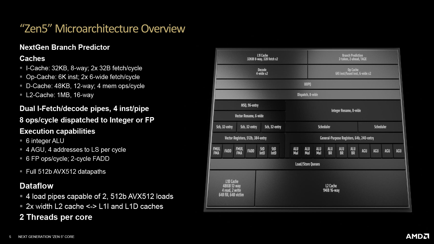
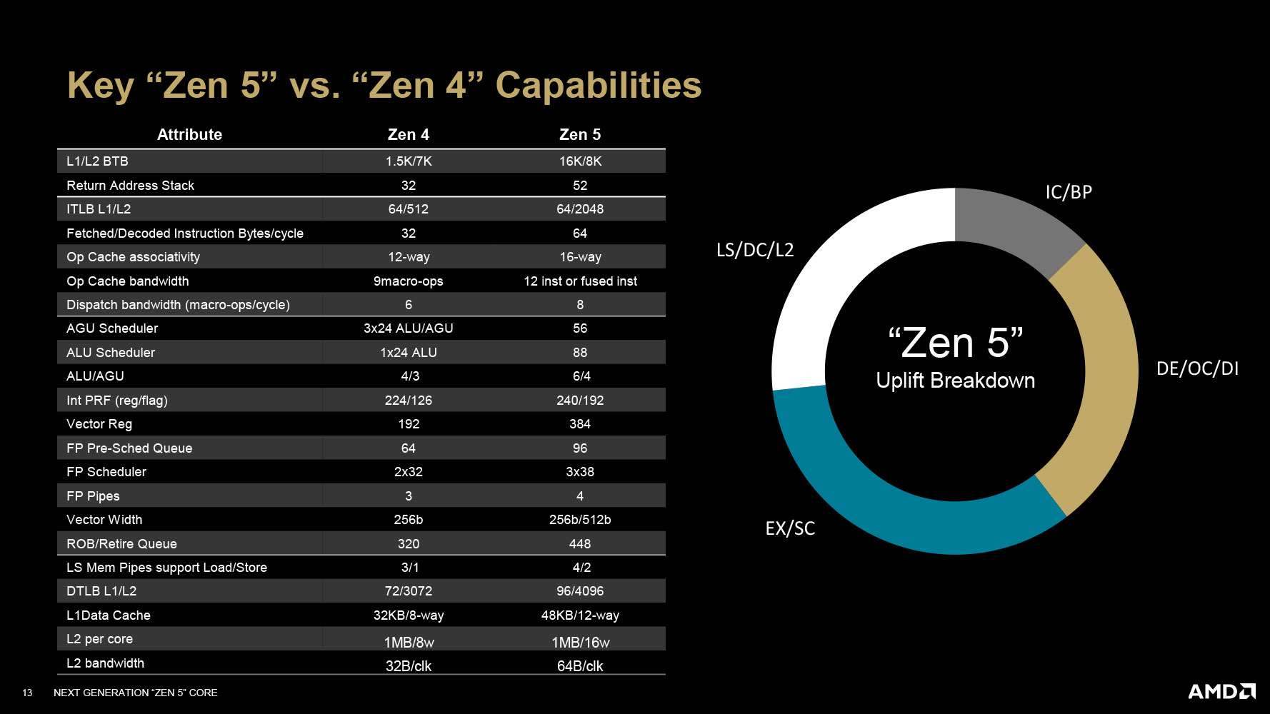
With Zen 5, AMD has updated practically all key areas of the CPU core, including the front-end with its branch prediction unit, the various caches within the core, the fetch/decode pipelines, the execution engine, and the load/store. The front-end sees an updated branch prediction unit. This new BP ensures zero-bubble conditional branches to save clock cycles from mispredictions; a large 16 KB L1 BTB, and a larger tagged-geometric length predictor; a larger 52-entry return address stack, compared to 32-entry on Zen 4; a 16-way Op Cache associativity, compared to 12-way on Zen 4, and a 33% increase in Op Cache and dispatch bandwidth. The BP supports up to 3 prediction windows per cycle, compared to 2 on Zen 4. The L2 and tablewalker latency is obscured with the new aggressive fetch unit. The L2 ITLB supports 2,048 entries, compared to just 512 on the Zen 4 core. The L1 instruction cache gets bandwidth and latency improvements, along with two independent instruction fetch streams.
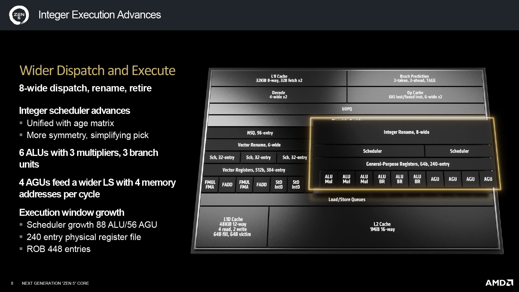
As with every traditional x86 CPU core, there's a split into Integer and Floating Point units. The Integer engine features an 8-wide dispatch/retire/rename queue depth. The integer scheduler has more "symmetry" to simplify pick operations. It features 6 ALUs with 3 multipliers, and 3 branch units; besides 4 AGUs. The AGU scheduler supports 56 entries, and the ALU scheduler 88, compared to 3x 24-entry ALU+AGU combined scheduling, with a 24-entry dedicated ALU scheduler. The physical register file is up to 240/192 entries from 224/126 on Zen 4. The ROB retire queue buffer holds 448 entries, compared to 320 on Zen 4.
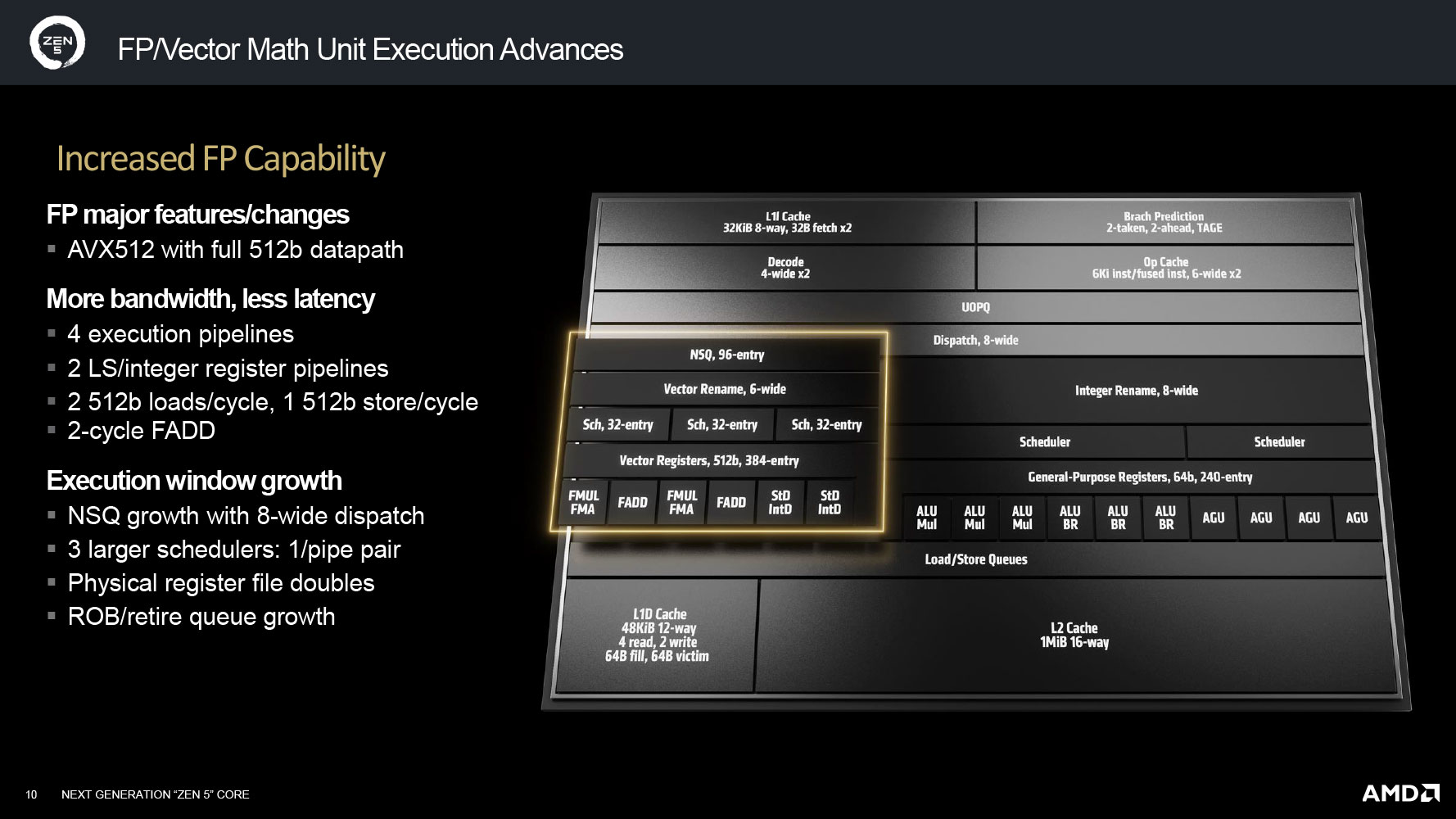
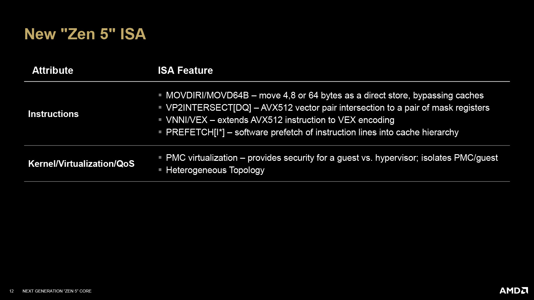
The floating point unit is where Zen 5 seems to have a major design focus. Zen 5 is designed to execute AVX-512 instructions over a full 512-bit data-path, compared to Zen 4, which uses a dual-pumped 256-bit data-path. This should significantly speed up AVX-512, VNNI, and other instructions relevant to AI acceleration on the CPU core. The FPU has four execution pipelines with two LS/integer register pipes. It supports two 512-bit loads, one 512-bit store per cycle, and a 2-cycle FADD. There are updates to the FPU's execution window.

The load/store unit sees several improvements to meet the growth in bandwidth requirements of the execution engine. To begin with, the L1 data cache has been enlarged to 48 KB 12-way, up from 32 KB 8-way on Zen 4. Besides this enlargement, there are improvements to the load/store pipes, with a mix of 4 loads and 2 stores per cycle. Its four integer load pipes can pair into FP pipe. The bandwidth to the L2 cache has been improved.
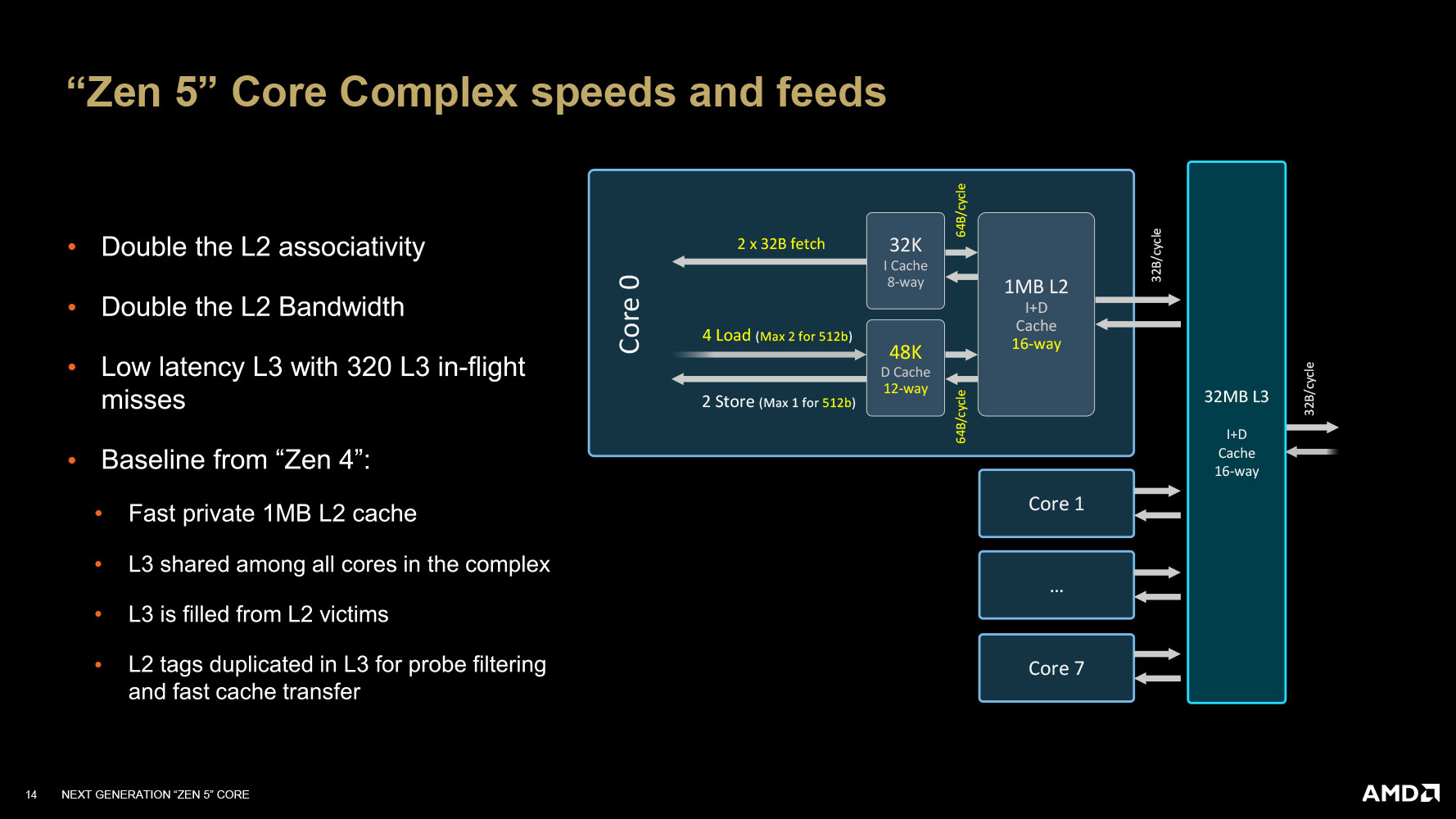
The core's dedicated L2 cache remains 1 MB in size from the previous generation, but AMD says that it has doubled the associativity and bandwidth of this cache over the one Zen 4 comes with. While AMD has retained 32 MB as the standard on-die L3 cache size, which it shares among the 8 cores on the CCD, it has worked to reduce the cache's latency along with tracking up to 320 L3 in-flight misses.
Granite Ridge SoC Features

Depending on the processor model, the chip features one or two CCDs, each with eight Zen 5 cores, 32 MB of L3 cache, an SMU, and an Infinity Fabric interface, with 32 B/cycle read and 16 B/cycle write bandwidth, to the client I/O die (cIOD). The cIOD uses Infinity Fabric to connect all the various SoC components of the processor, the two most important of which are the dual-channel DDR5 memory controllers (160-bit including ECC), and the 28-lane PCI-Express 5.0 root complex.
AMD provides a basic iGPU with Granite Ridge, just like it did with Raphael. This is based on the older RDNA 2 graphics architecture due to reusing the cIOD from Zen 4, and consists of just one workgroup processor (WGP), or just two compute units (CU), worth 128 stream processors. This iGPU talks to a display controller that supports up to four displays; and a multimedia engine that can accelerate decode of H.265 and AV1.
There's also an integrated USB interface, with support for USB 3.2 (up to two 10 Gbps ports), a couple of USB 2.0 ports, and legacy interfaces, including SPI, eSPI, GPIO, I2C, etc. The client I/O die is built on the 6 nm foundry node, as many of these components don't really benefit from the latest 4 nm node. The cIOD of Granite Ridge is carried over from Raphael, with only some microcode updates that give it native support for DDR5-5600 (Ryzen 7000 natively supported DDR5-5200), various overclocking speeds over AMD EXPO, and support for higher DDR5 overclocking memory speeds using a 1:2 divider between the FCLK and MCLK.
AMD X870E, X870, B850, and B840 Chipsets
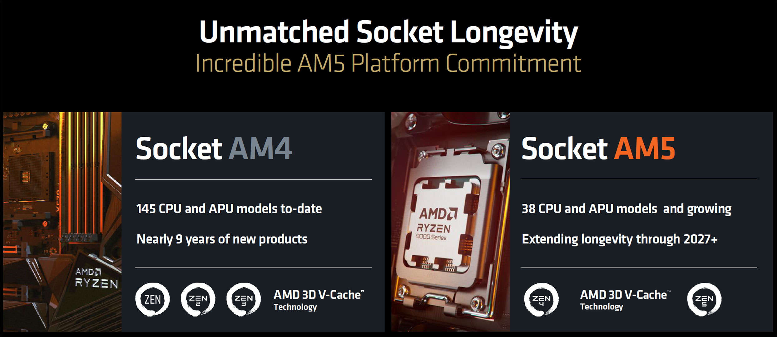
Along with the Ryzen 9000 Granite Ridge series, AMD is debuting their 800 series desktop motherboard chipset family. The processors are placed in the existing Socket AM5, and as such are compatible with any AMD 600-series chipset motherboard with a BIOS update. Helping things along is the fact that nearly every AM5 motherboard comes with USB BIOS Flashback, which should let you blind-flash your BIOS even if you have an "incompatible" processor.
AMD hasn't changed the I/O of its processors, as we detailed on the previous page, but identified the reasons why some of its 600-series chipset models were vastly outselling the others. Market studies showed that enthusiasts are drawn to the top X670E, and the rest of the crowd to the well-rounded B650, with no takers for the X670 and B650E. AMD set out to correct these by shuffling up the feature-sets among its 800-series chipset models, while also using the occasion to standardize a few I/O features, such as USB4, and encouraging its motherboard partners to provide new connectivity options, such as Wi-Fi 7.

The AMD X870E chipset leads the pack in terms of connectivity. It is a dual-chip solution, much like X670E and X670. You are assured PCI-Express Gen 5 for the x16 PEG slot, as well as the CPU-attached NVMe slots; while the chipset puts out up to 16 Gen 4 PCIe lanes. Also, motherboard designers are mandated to provide 40 Gbps USB4 connectivity.
The X870 (non-E) is a lite version of this chipset, and is a single-chip solution, much like the B650E. You'll still get PCI-Express Gen 5 x16 for the PEG slot, as well as Gen 5 for the CPU-attached NVMe slots, however the chipset only puts out 8 Gen 4 PCIe lanes for general purpose I/O. Much like X870E, with X870 you are assured of USB4 connectivity.
The B850 is a successor of the B650. It is a single-chip solution just like X870, but here, motherboard vendors are allowed to wire out the PCI-Express x16 PEG slot as Gen 4. The CPU-attached NVMe interfaces, however, should remain Gen 5 capable. Motherboard vendors can still provide Gen 5 x16 PEG if they want to, but it's optional. USB4 isn't mandatory, so a vendor can design an X870 motherboard and simply pull out the USB4 interface to label the board as B850. Like X870E and X870, the B850 chipset supports both CPU and memory overclocking.
Lastly, there's the B840, an entry-level chipset meant to succeed the A620 and A620A. The PCI-Express x16 PEG runs at a primitive Gen 3 speed. The chipset puts out just 8 Gen 3 lanes. There's no CPU overclocking support, only memory. The B840 should hence power the vast majority of entry-level or commercial desktop motherboards.
Overclocking

Curve Shaper is a new feature being introduced with Ryzen 9000 series processors. It's part of the AMD CBS, which means it can be configured in the UEFI setup program, should the motherboard vendor choose to have a GUI there, or using Ryzen Master on Windows. Curve Optimizer enabled PBO and PMF-aware under-volting, while Curve Shaper lets end-users reshape the underlying voltage curves to fine tune voltage control across different workloads and frequencies.

A side effect of giving processor models such as the 9900X (120 W), 9700X (65 W), and 9600X lower TDP than their predecessors, the 7900X (170 W), and 7700X (105 W), is that Precision Boost Overdrive (PBO) now scoops out more performance, as it raises the package power for the processors. AMD claims further performance gains of 6% for the 9900X, and up to 15% for the 9700X (which goes to show that 65 W is quite conservative for this SKU).

Native DDR5 support has been increased to DDR5-5600, and support has been added for overclocked memory as fast as DDR5-8000. To achieve this, a 1:2 clock divider is engaged between FCLK and MCLK as soon as memory clock is set higher than DDR5-6000. You may manually force a 1:1 divider "and with some luck" you will be able to run DDR5-6400—essentially the same as with Zen 4. DDR5-8000 support has been released by AMD through an update to the AGESA microcode, for motherboard vendors to integrate with even their older AMD 600-series chipset products. There should be a new wave of enthusiast PC memory with AMD EXPO profiles for DDR5-8000 and everything under (such as DDR5-7200, DDR5-6800, etc.). In terms of performance it is interesting to see if DDR5-8000 1:2 can beat DDR5-6000 1:1 in a wide range of scenarios, which could make it a worthwhile investment. TPU has tested Zen 5 memory scaling in a separate article.
Socket AM5

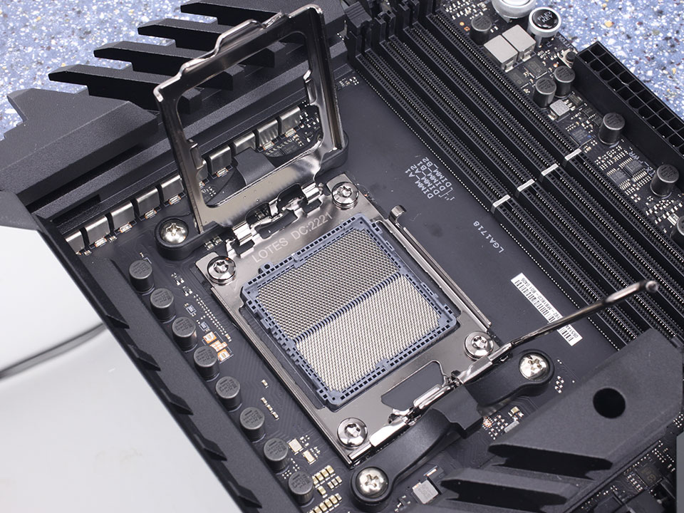
Here are a few pictures of Socket AM5, the star-attraction with this platform. This is a land-grid array (LGA) socket with 1,718 pins.

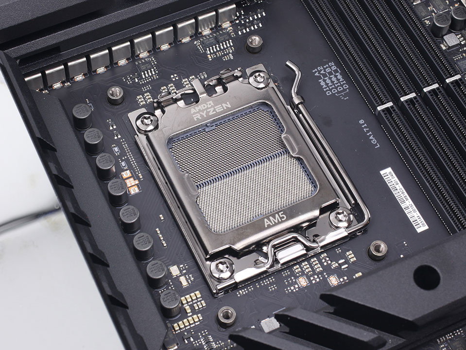
As with every LGA socket, the pins are on the motherboard, whereas the processor package has contacts that interface with those pins, while a retention brace holds the package in place with a locking lever. Installing a processor on AM5 is similar to doing so on any of the dozens of Intel LGA sockets.


On Socket AM4, removing the four mounting screws resulted in the backplate falling off, which meant you needed three hands when installing a cooler, and several vendors also bundled their own backplates. On Socket AM5 the backplate isn't designed to be removed, which makes cooler installation MUCH easier.

The caps for the socket are not identical to the Intel LGA sockets, so you can't reuse them.
Unboxing and Photography
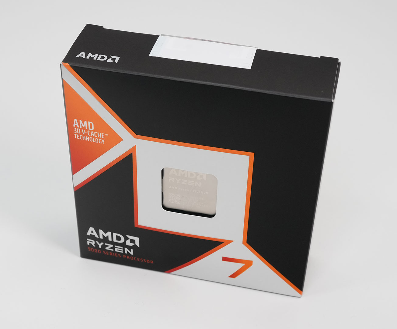
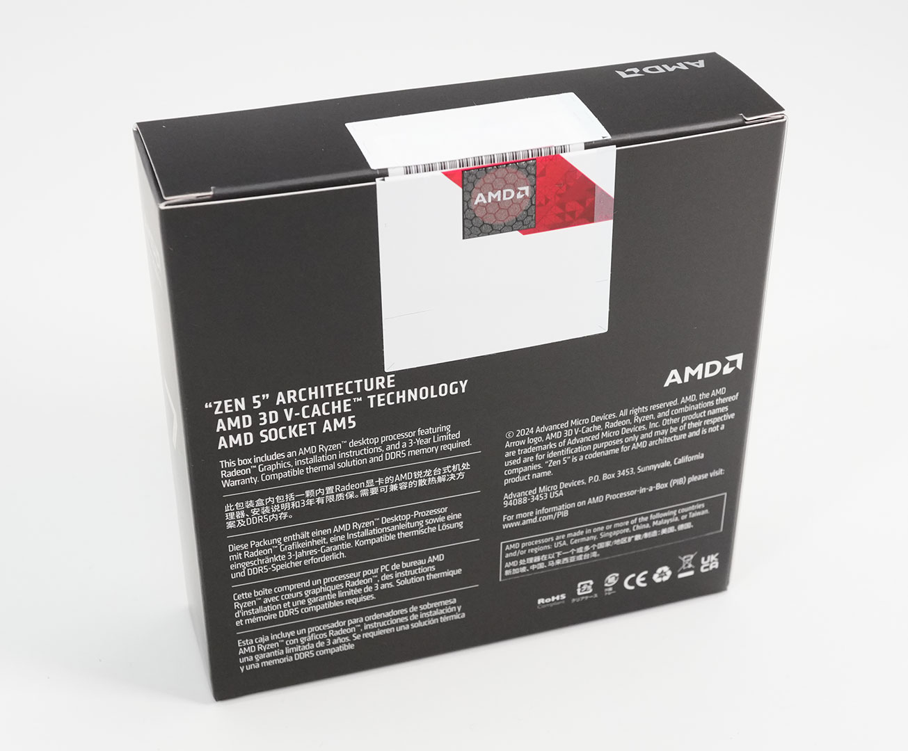
The Ryzen 7 9800X3D comes in a square-shaped box, similar to the other Ryzen 9000 series chips. There's no included cooling solution. The box-art is a slight variation on the theme set by the regular Ryzen 9000 series chips, the AMD arrow is now set against a silver backdrop instead of gray. There's clear marking on the front and back faces that the processor features 3D V-Cache technology.
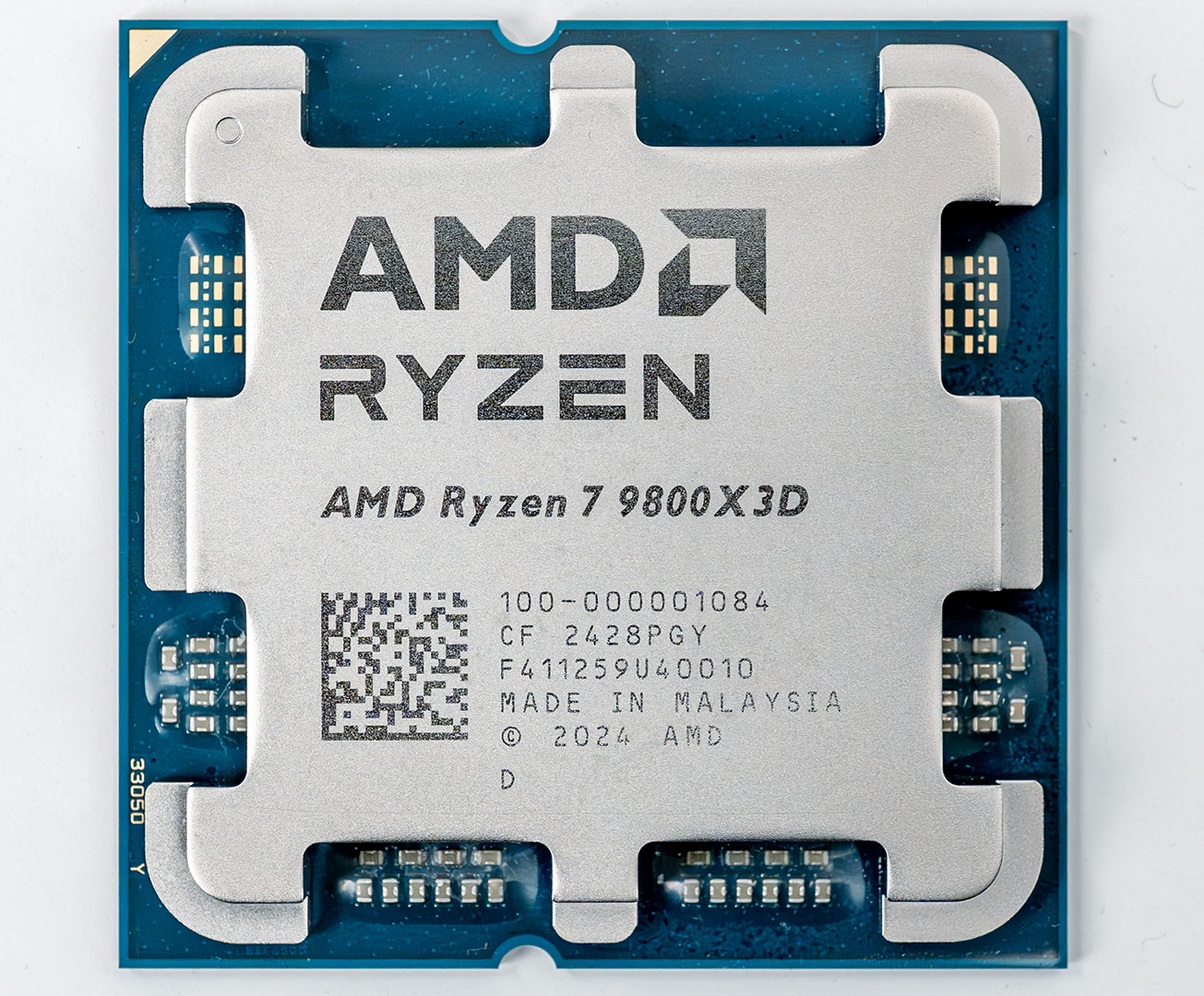

The new Ryzen 9000 Series looks just like the previous Ryzen 7000 Socket AM5 processors. While there are some minimal changes to the SMD capacitor layout, these aren't significant in any way.
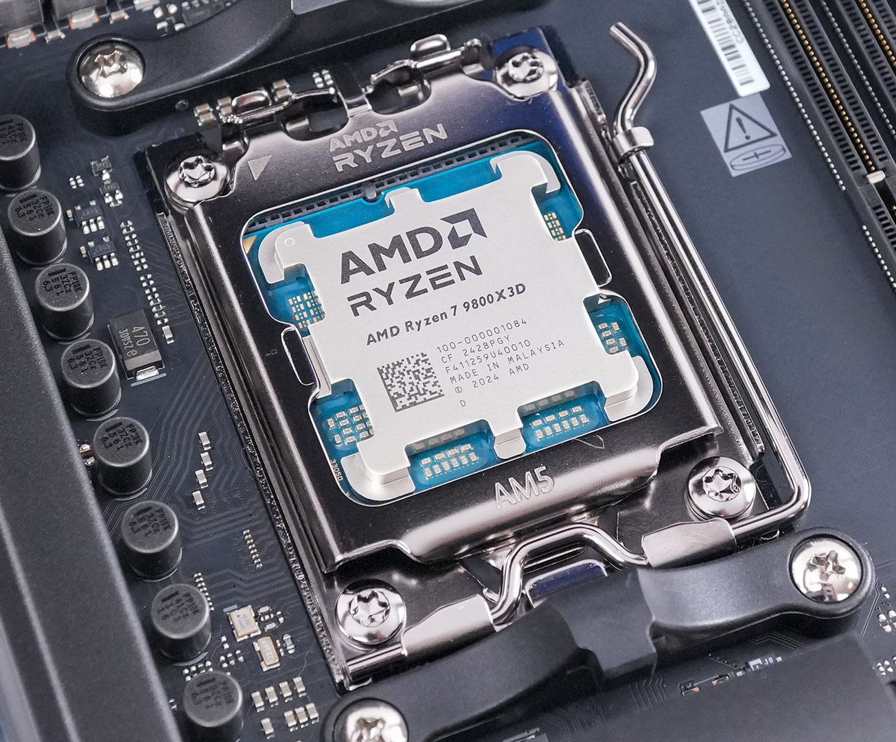
The AM5 socket retention brace only applies pressure along the two side protrusions of the IHS. Intel sockets have it the same way. Socket AM5 retains cooler compatibility with AM4, so you're spoiled for choice with aftermarket cooling solutions.
Test Setup
- All applications, games, and processors are tested with the drivers and hardware listed below—no performance results were recycled between test systems.
- All games and applications are tested using the same version.
- All games are set to their highest quality setting unless indicated otherwise.
- Now that DDR5 has gained some maturity, we will use faster DDR5 speeds with tighter timings in upcoming reviews (once we retest the 40+ CPUs in our test group)
- As little preview of that, we're including an additional benchmark run at DDR5-6200 UCLK 1:1 CL28 in this review (red bar)
| Test System "Zen 4 & Zen 5" | |
|---|---|
| Processor: | All AMD Ryzen 9000, 8000 & Ryzen 7000 processors |
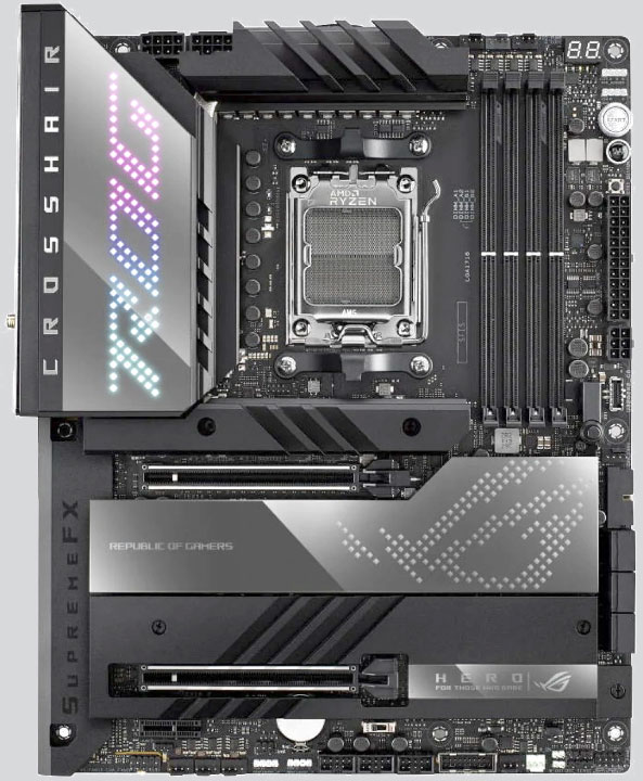
| Motherboard: | ASUS X670E Crosshair Hero BIOS 2007 Ryzen 9000: BIOS 2201 9800X3D: ASUS X870E Crosshair Hero BIOS 0605 |
| Memory: | 2x 16 GB DDR5-6000 36-36-36-76 Infinity Fabric @ 2000 MHz |
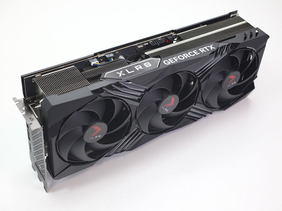
| Graphics: | PNY GeForce RTX 4090 XLR8 |
| Storage: | 2 TB M.2 NVMe SSD |
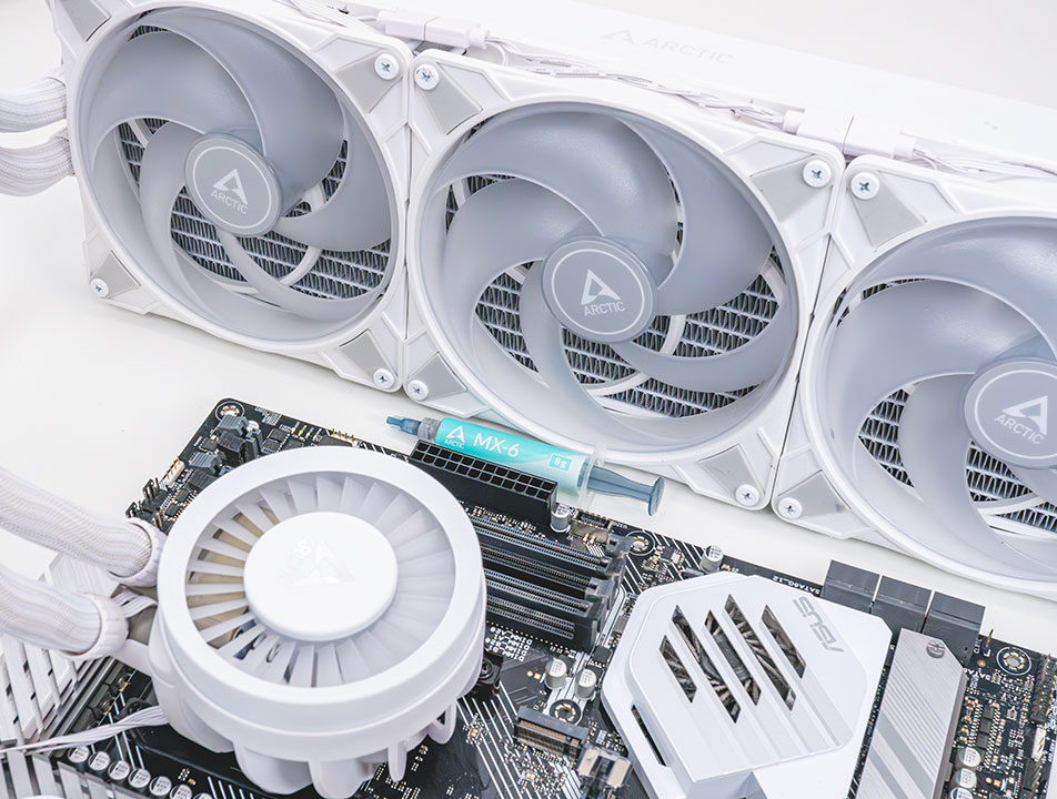
| Air Cooling: | Noctua NH-D15 |
| Water Cooling: | Arctic Liquid Freezer III 420 mm AIO |
| Thermal Paste: | Arctic MX-6 |
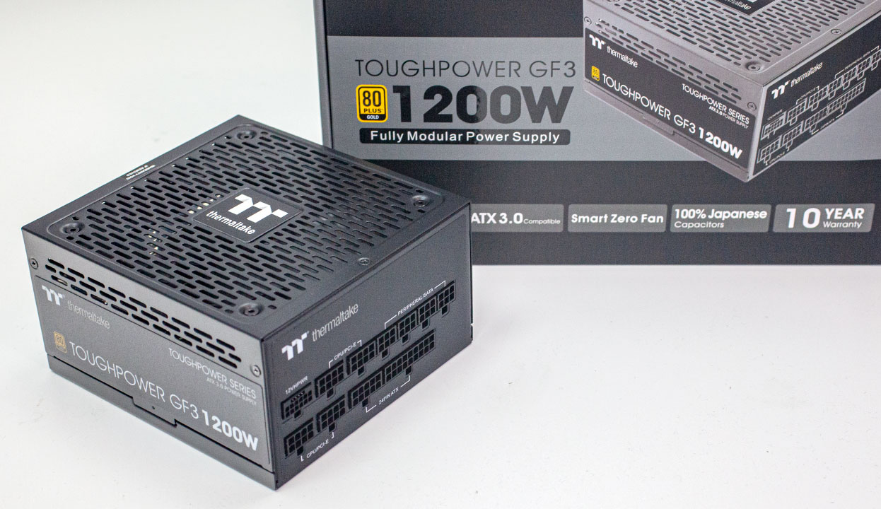
| Power Supply: | Thermaltake Toughpower GF3 1200 W ATX 3.0 / 16-pin 12VHPWR |
| Software: | Windows 11 Professional 64-bit 23H2 VBS enabled (Windows 11 default) |
| Drivers: | Ryzen Chipset Drivers 6.05.28.016 Ryzen 9000: 6.06.28.910 Ryzen 9800X3D: 6.09.25.044 Ryzen 9000: Game Mode enabled, Game Bar installed and active |
| Test System "Arrow Lake" | |
|---|---|
| Processor: | All Intel Core 200 Series processors (Intel stock power settings / ASUS MCE disabled) |
| Motherboard: | ASUS Z890 Maximus Hero BIOS 0805 MSI Z890 Carbon (power consumption tests) BIOS 1A2T |
| Memory: | 2x 16 GB DDR5-6000 36-36-36-76 2T / Gear 2 |
| All other specifications same as above | |
| Test System "Raptor Lake & Alder Lake" | |
|---|---|
| Processor: | All Intel 14th, 13th & 12th Gen processors (Intel stock power settings / ASUS MCE disabled) |
| Motherboard: | ASUS Z790 Maximus Dark Hero BIOS 1302 |
| Memory: | 2x 16 GB DDR5-6000 36-36-36-76 2T / Gear 2 |
| All other specifications same as above | |
| Test System "Zen 3 & Zen 2" | |
|---|---|
| Processor: | All AMD Ryzen 5000 & Ryzen 3000 processors |
| Motherboard: | ASUS X570 Crosshair VII Dark Hero BIOS 4805 |
| Memory: | 2x 16 GB DDR4-3600 14-14-14-34 1T Infinity Fabric @ 1800 MHz 1:1 |
| Drivers: | Ryzen Chipset Drivers 6.05.28.016 |
| All other specifications same as above | |
| Test System "Rocket Lake" | |
|---|---|
| Processor: | All Intel 11th Gen processors (Intel stock power settings / ASUS MCE disabled) |
| Motherboard: | ASUS Z590 Maximus XIII Hero BIOS 1701 |
| Memory: | 2x 16 GB DDR4-3600 14-14-14-34 1T Gear 1 |
| All other specifications same as above | |
| Test System "Zen 1" | |
|---|---|
| Processor: | All AMD Ryzen 2000 processors |
| Motherboard: | ASUS X570 Crosshair VII Dark Hero BIOS 4805 |
| Memory: | 2x 16 GB DDR4-3400 14-14-14-34 1T |
| All other specifications same as above | |
AIDA64 Cache and Memory Performance
In this first test we're looking at the performance offered by the memory subsystem and the processor's L1, L2 and L3 caches. AIDA64 comes with a great benchmark that provides a nice overview of all these performance characteristics.
Our Patreon Silver Supporters can read articles in single-page format.
Apr 17th, 2025 05:54 EDT
change timezone
Latest GPU Drivers
New Forum Posts
- Can,t download Windows 11 or 10. (3)
- Is it worth buying a pi5 with a broken hdmi connector (5)
- Intel Iris XE Graphics Driver Issue. (6)
- my new mini pc (0)
- RX 9000 series GPU Owners Club (347)
- [REQUEST] Palit RTX 5080 GameRock OC ver. bios (6)
- The TPU UK Clubhouse (26131)
- RTX5000 Series Owners Club (173)
- Throttlestop 9.7.3 Legion 7 Pro 13900HX, RTX4090 locking frequency issue (2)
- ThrottleStop Settings i7-10750H (0)
Popular Reviews
- G.SKILL Trident Z5 NEO RGB DDR5-6000 32 GB CL26 Review - AMD EXPO
- ASUS GeForce RTX 5060 Ti TUF OC 16 GB Review
- NVIDIA GeForce RTX 5060 Ti PCI-Express x8 Scaling
- ASUS GeForce RTX 5080 TUF OC Review
- DAREU A950 Wing Review
- Palit GeForce RTX 5060 Ti Infinity 3 16 GB Review
- ASUS GeForce RTX 5060 Ti Prime OC 16 GB Review
- Zotac GeForce RTX 5060 Ti AMP 16 GB Review
- The Last Of Us Part 2 Performance Benchmark Review - 30 GPUs Compared
- MSI GeForce RTX 5060 Ti Gaming OC 16 GB Review
Controversial News Posts
- NVIDIA GeForce RTX 5060 Ti 16 GB SKU Likely Launching at $499, According to Supply Chain Leak (182)
- NVIDIA Sends MSRP Numbers to Partners: GeForce RTX 5060 Ti 8 GB at $379, RTX 5060 Ti 16 GB at $429 (127)
- Nintendo Confirms That Switch 2 Joy-Cons Will Not Utilize Hall Effect Stick Technology (105)
- Over 200,000 Sold Radeon RX 9070 and RX 9070 XT GPUs? AMD Says No Number was Given (100)
- Nintendo Switch 2 Launches June 5 at $449.99 with New Hardware and Games (99)
- NVIDIA Launches GeForce RTX 5060 Series, Beginning with RTX 5060 Ti This Week (92)
- Sony Increases the PS5 Pricing in EMEA and ANZ by Around 25 Percent (85)
- NVIDIA PhysX and Flow Made Fully Open-Source (77)