 68
68
ASUS GeForce GTX 470 Fermi Review
(68 Comments) »Introduction
A few weeks back NVIDIA launched what is certainly the most anticipated graphics card series this year. The NVIDIA GeForce GTX 470 and 480 are based on NVIDIA's new Fermi architecture which is a complete overhaul of the GT200 architecture. The cards offer full support for DirectX 11 and Tesselation, as well as 3D Vision Surround for multi-monitor gaming in 3D.

The GeForce GTX 470 is based on the same Fermi core as the GTX 480 but uses a reduced shader count and less memory bus width. In the image above, you can see the disabled components of the GF100 GPU. Please note that the red rectangles can be any SM or any MC, not specifically the marked ones. This allows NVIDIA to harvest more GPUs from their production which results in a more economic end-user pricing of the product.
ASUS has sent us a final retail sample of GeForce GTX 470.
| Radeon HD 4870 X2 | GeForce GTX 285 | Radeon HD 5850 | GeForce GTX 470 | Radeon HD 5870 | GeForce GTX 480 | GeForce GTX 295 | Radeon HD 5970 | |
| Shader units | 2x 800 | 240 | 1440 | 448 | 1600 | 480 | 2x 240 | 2x 1600 |
| ROPs | 2x 16 | 32 | 32 | 40 | 32 | 48 | 2x 28 | 2x 32 |
| GPU | 2x RV770 | GT200b | Cypress | GF100 | Cypress | GF100 | 2x GT200b | 2x Cypress |
| Transistors | 2x 956M | 1400M | 2154M | 3200M | 2154M | 3200M | 2x 1400M | 2x 2154M |
| Memory Size | 2x 1024 MB | 1024 MB | 1024 MB | 1280 MB | 1024 MB | 1536 MB | 2x 896 MB | 2x 1024 MB |
| Memory Bus Width | 2x 256 bit | 512 bit | 256 bit | 320 bit | 256 bit | 384 bit | 2x 448 bit | 2x 256 bit |
| Core Clock | 750 MHz | 648 MHz | 725 MHz | 607 MHz | 850 MHz | 700 MHz | 576 MHz | 725 MHz |
| Memory Clock | 900 MHz | 1242 MHz | 1000 MHz | 837 MHz | 1200 MHz | 924 MHz | 999 MHz | 1000 MHz |
| Price | $350 | $350 | $310 | $349 | $400 | $499 | $520 | $630 |
Packaging & Contents
We received a retail card, but without packaging and accessories.The Card

NVIDIA has managed to keep the GTX 470 to a more compact form factor than the GTX 480.

This sticker adds a carbon-fibre look to the card, really amazing. In my opinion this approach is a much better solution that adding some poorly printed anime girl sticker.
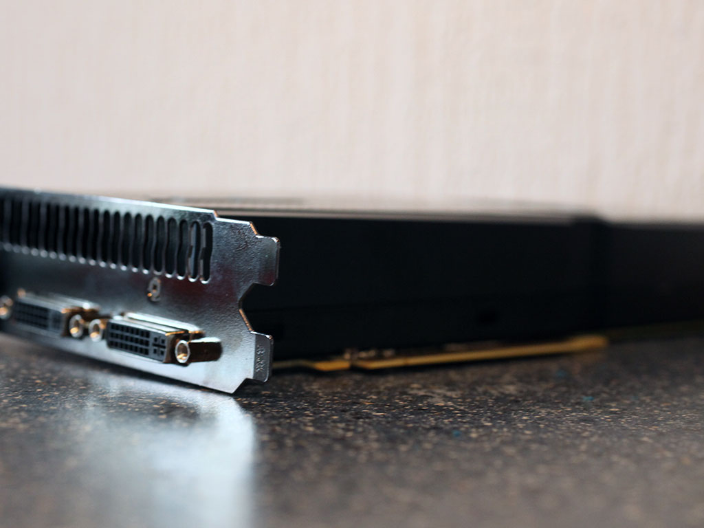
Just like the reference design cards, you need two slots in your system for installation.
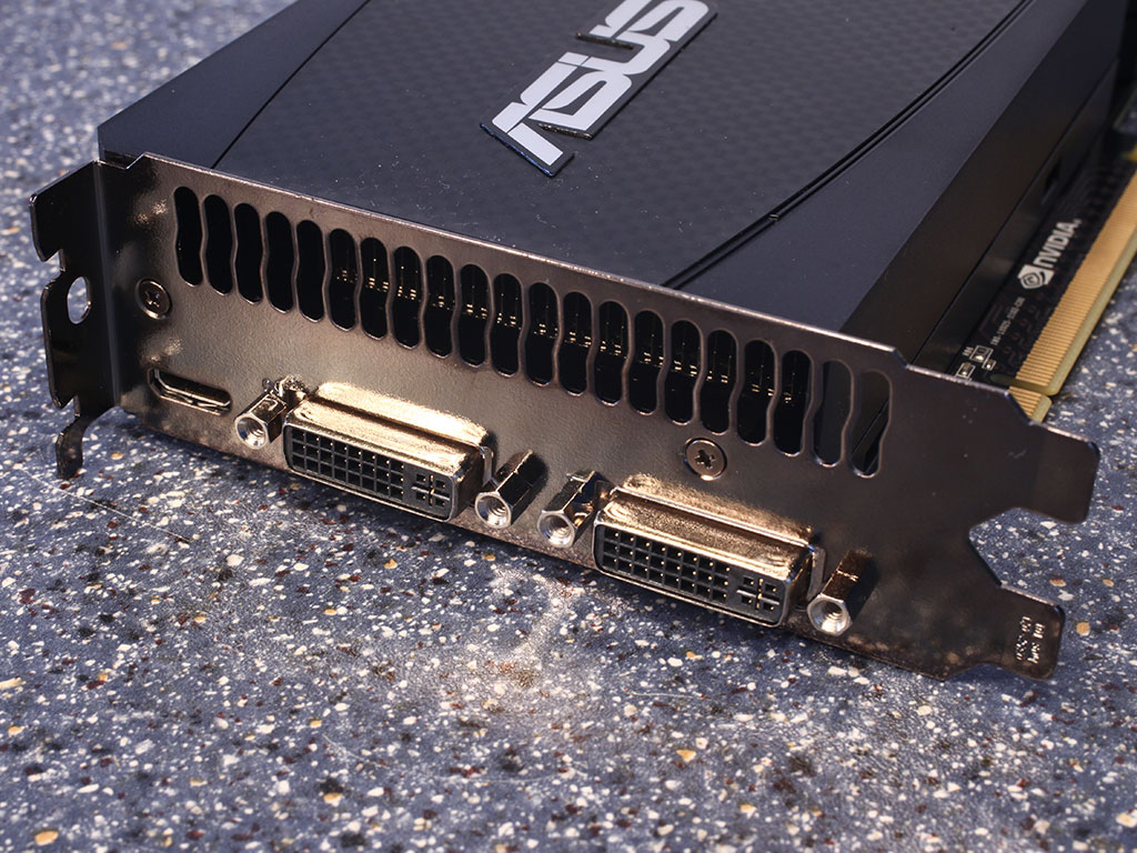
The card has two DVI ports and one one mini-HDMI port. According to NVIDIA the card also supports DisplayPort if board partners want to use it. Unlike AMD's latest GPUs, the output logic design is not as flexible. On AMD cards vendors are free to combine six TMDS links into any output configuration they want (dual-link DVI consuming two links), from what we know so far, on NVIDIA, you are fixed to two DVI outputs and one HDMI/DP in addition to that. NVIDIA confirmed that you can use only two displays at the same time, so for a three monitor setup you would need two cards.
NVIDIA has included an HDMI sound device inside their GPU which does away with the requirement of connecting an external audio source to the card for HDMI audio. The HDMI interface is HDMI 1.3a compatible which includes Dolby TrueHD, DTS-HD, AC-3, DTS and up to 7.1 channel audio with 192 kHz / 24-bit. NVIDIA also claims full support for the 3D portion of the HDMI 1.4 specification which will become important later this year when we will see first Blu-Ray titles shipping with support for 3D output.
SLI with any other GTX 470 card (from any board partner) is possible to improve performance.


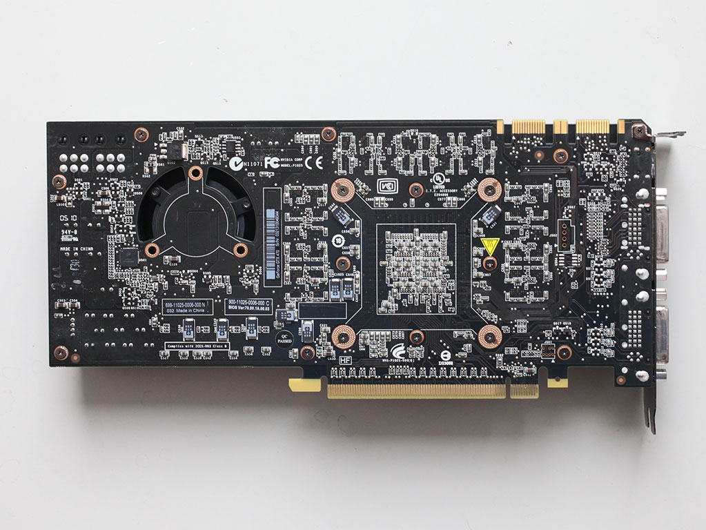
Here are the front and the back of the card, high-res versions are also available (front, back). If you choose to use these images for voltmods etc, please include a link back to this site or let us post your article.
A Closer Look


The first step in disassembly is removing the black plastic fan shroud. It is a simple piece of plastic that protects the heatsink and creates an air channel for the fan's air to move out of the card.


You will find five heatpipes on the main heatsink that use DirectTouch technology to make optimum contact with the GPU core. Heat is then transferred to a large number of fins where it is dissipated.


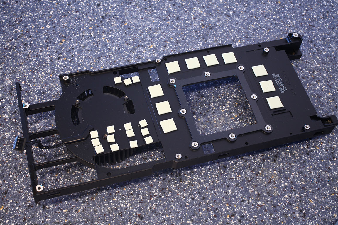
The last piece that goes off is a big black metal heatsink that covers all the "minor" components of the graphics card, like memory and voltage regulation circuitry. This approach makes it easy for water cooling and extreme cooling to be attached to the GPU only without having to worry about cooling the rest of the components.

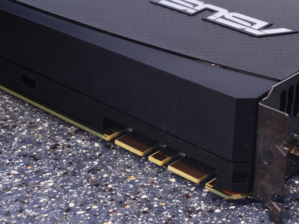
Dual six-pin power connectors are already a first hint that the power consumption of the GeForce GTX 470 isn't going to be as epic as that of the GTX 480.

The GDDR5 memory chips are made by Samsung, and carry the model number K4G10325FE-HC05. They are specified to run at 2000 MHz (4000 MHz GDDR5 effective).
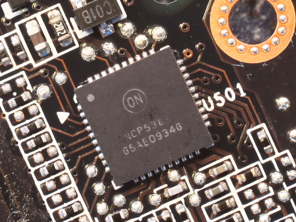
OnSemi's NCP5388 is a reasonable priced voltage regulator, unfortunately it does not have I2C voltage control.

NVIDIA's GeForce 100 graphics processor is made on a 40 nm process at TSMC Taiwan. It uses approximately 3.2 billion transistors which makes it the most complex GPU built to-date. Please note that the silvery metal surface you see is the heatspreader of the GPU which measures 42.3 x 42.3 mm. The actual GPU die is sitting under the heatspreader, its dimensions are not known. NVIDIA did not communicate a die size measurement to the press.
Our Patreon Silver Supporters can read articles in single-page format.
Apr 24th, 2025 00:14 EDT
change timezone
Latest GPU Drivers
New Forum Posts
- Which is the best replacement for Microsoft Office? (23)
- RX 9000 series GPU Owners Club (500)
- Asus Rx570 o4g cannot losd drivers error code 43 (13)
- How do you calculate the cost of a chip? (4)
- need help with 12900hx (6)
- Are the 8 GB cards worth it? (108)
- 5060 Ti 8GB DOA (257)
- Help getting a mini pc (7)
- 5070ti overclock...what are your settings? (16)
- New GPU 5070 Ti or better CPU Ryzen7 7800X3D ? (6)
Popular Reviews
- NVIDIA GeForce RTX 5060 Ti 8 GB Review - So Many Compromises
- ASUS GeForce RTX 5060 Ti TUF OC 16 GB Review
- ASRock X870E Taichi Lite Review
- Colorful iGame B860M Ultra V20 Review
- Upcoming Hardware Launches 2025 (Updated Apr 2025)
- Sapphire Radeon RX 9070 XT Pulse Review
- Sapphire Radeon RX 9070 XT Nitro+ Review - Beating NVIDIA
- NVIDIA GeForce RTX 5060 Ti PCI-Express x8 Scaling
- AMD Ryzen 7 9800X3D Review - The Best Gaming Processor
- ASUS GeForce RTX 5080 TUF OC Review
Controversial News Posts
- NVIDIA GeForce RTX 5060 Ti 16 GB SKU Likely Launching at $499, According to Supply Chain Leak (182)
- NVIDIA Sends MSRP Numbers to Partners: GeForce RTX 5060 Ti 8 GB at $379, RTX 5060 Ti 16 GB at $429 (127)
- NVIDIA Launches GeForce RTX 5060 Series, Beginning with RTX 5060 Ti This Week (115)
- Nintendo Confirms That Switch 2 Joy-Cons Will Not Utilize Hall Effect Stick Technology (105)
- Nintendo Switch 2 Launches June 5 at $449.99 with New Hardware and Games (99)
- Sony Increases the PS5 Pricing in EMEA and ANZ by Around 25 Percent (85)
- NVIDIA PhysX and Flow Made Fully Open-Source (77)
- Windows Notepad Gets Microsoft Copilot Integration (75)