 296
296
ASUS GeForce RTX 4070 Ti TUF Review
(296 Comments) »Introduction
ASUS TUF Gaming GeForce RTX 4070 Ti OC is the company's affordable custom-design implementation of the brand new performance-segment GPU by NVIDIA, positioned a notch below its ROG Strix series. The TUF Gaming brand of graphics cards gained prominence with the RTX 30-series "Ampere" for striking a great balance between the product design gamers want, and a value feature-set that covers all the essentials, rounding up a solid, reliable package. With the RTX 40-series "Ada," ASUS is sticking to this formula, by giving this card a "tough" industrial product feel, with a design focus on a well-ventilated cooling solution, a minor factory-overclock, and durability you come to expect from ASUS. For flashy RGB lighting, fan-headers, and other such goodies, you should seek out the ROG Strix products.

NVIDIA GeForce RTX 4070 Ti is the company's third desktop RTX 40-series "Ada" graphics card, and its launch in early January has a bit of a controversial story attached to it. This SKU was formerly regarded as the "RTX 4080 12 GB," and was supposed to launch mid-November 2022, alongside a 16 GB sibling bearing the same "RTX 4080" model number. It turned out that the two SKUs were vastly different—not counting the memory size—, and that the RTX 4080 12 GB was based on a physically smaller silicon, with 21% fewer shaders, RT cores, and Tensor cores; and its memory bus was 25% narrower, besides the reduction in memory size. This would've meant that a vast performance gap would emerge between the 12 GB and 16 GB models, and since the 12 GB would still bear the "4080" branding, NVIDIA could price it as high as $900 (MSRP). After some pushback on social media and the press, NVIDIA decided to cancel the RTX 4080 12 GB, and re-launch it today as the RTX 4070 Ti, at a slightly lower starting price of $800.
We already know the specs of this card from NVIDIA's November 2022 announcement of the RTX 4080 series. The card is based on the 5 nm "AD104" silicon, NVIDIA's third-biggest chip based on the "Ada" graphics architecture. The RTX 4070 Ti maxes it out, enabling all 7,680 CUDA cores across 60 SM, along with 60 RT cores, 240 Tensor cores, 240 TMUs, and 80 ROPs. The card gets 12 GB of memory across a 192-bit wide GDDR6X memory interface, which ticks at 21 Gbps, working out to 504 GB/s of memory bandwidth, which may pale in comparison to the 760 GB/s of the RTX 3080 10 GB (similar launch MSRP), or the 608 GB/s of the RTX 3070 Ti, but NVIDIA claims to have straightened out many of its memory performance bottlenecks at the architecture-level, with much larger on-die caches on the GPU.
The ASUS TUF Gaming RTX 4070 Ti OC comes with a slightly lighter version of the TUF Gaming "Vented Exoskeleton" cooling solution that minimizes the cooler shroud in favor of large vents for the heatsink underneath to vent out exhaust. The card is strictly 3 slots thick, compared to the 3.5-slot RTX 4080 TUF Gaming. With this generation, NVIDIA is standardizing the ATX 12VHPWR power connector, even in this segment of the market. The card also comes with a nifty little factory overclock, with the GPU Boost set at 2730 MHz, compared to 2610 MHz reference, and the memory untouched at 21 Gbps. ASUS is pricing the card at a $50 premium over the $800 baseline pricing.
Short 10-Minute Video Comparing 10x RTX 4070 Ti Super
Our goal with the videos is to create short summaries, not go into all the details and test results, which can be found in our written reviews.
| Price | Cores | ROPs | Core Clock | Boost Clock | Memory Clock | GPU | Transistors | Memory | |
|---|---|---|---|---|---|---|---|---|---|
| RTX 2080 | $380 | 2944 | 64 | 1515 MHz | 1710 MHz | 1750 MHz | TU104 | 13600M | 8 GB, GDDR6, 256-bit |
| RTX 3060 Ti | $410 | 4864 | 80 | 1410 MHz | 1665 MHz | 1750 MHz | GA104 | 17400M | 8 GB, GDDR6, 256-bit |
| RX 6700 XT | $360 | 2560 | 64 | 2424 MHz | 2581 MHz | 2000 MHz | Navi 22 | 17200M | 12 GB, GDDR6, 192-bit |
| RX 6750 XT | $470 | 2560 | 64 | 2495 MHz | 2600 MHz | 2250 MHz | Navi 22 | 17200M | 12 GB, GDDR6, 192-bit |
| RTX 2080 Ti | $600 | 4352 | 88 | 1350 MHz | 1545 MHz | 1750 MHz | TU102 | 18600M | 11 GB, GDDR6, 352-bit |
| RTX 3070 | $500 | 5888 | 96 | 1500 MHz | 1725 MHz | 1750 MHz | GA104 | 17400M | 8 GB, GDDR6, 256-bit |
| RTX 3070 Ti | $600 | 6144 | 96 | 1575 MHz | 1770 MHz | 1188 MHz | GA104 | 17400M | 8 GB, GDDR6X, 256-bit |
| RX 6800 | $510 | 3840 | 96 | 1815 MHz | 2105 MHz | 2000 MHz | Navi 21 | 26800M | 16 GB, GDDR6, 256-bit |
| RX 6800 XT | $650 | 4608 | 128 | 2015 MHz | 2250 MHz | 2000 MHz | Navi 21 | 26800M | 16 GB, GDDR6, 256-bit |
| RTX 3080 | $750 | 8704 | 96 | 1440 MHz | 1710 MHz | 1188 MHz | GA102 | 28000M | 10 GB, GDDR6X, 320-bit |
| RTX 3080 Ti | $950 | 10240 | 112 | 1365 MHz | 1665 MHz | 1188 MHz | GA102 | 28000M | 12 GB, GDDR6X, 384-bit |
| RX 6900 XT | $700 | 5120 | 128 | 2015 MHz | 2250 MHz | 2000 MHz | Navi 21 | 26800M | 16 GB, GDDR6, 256-bit |
| RX 6950 XT | $800 | 5120 | 128 | 2100 MHz | 2310 MHz | 2250 MHz | Navi 21 | 26800M | 16 GB, GDDR6, 256-bit |
| RTX 3090 | $950 | 10496 | 112 | 1395 MHz | 1695 MHz | 1219 MHz | GA102 | 28000M | 24 GB, GDDR6X, 384-bit |
| RTX 4070 Ti | $800 | 7680 | 80 | 2310 MHz | 2610 MHz | 1313 MHz | AD104 | 35800M | 12 GB, GDDR6X, 192-bit |
| ASUS RTX 4070 Ti TUF OC | $850 | 7680 | 80 | 2310 MHz | 2730 MHz | 1313 MHz | AD104 | 35800M | 12 GB, GDDR6X, 192-bit |
| RX 7900 XT | $900 | 5376 | 192 | 2000 MHz | 2400 MHz | 2500 MHz | Navi 31 | 57700M | 20 GB, GDDR6, 320-bit |
| RTX 3090 Ti | $1400 | 10752 | 112 | 1560 MHz | 1950 MHz | 1313 MHz | GA102 | 28000M | 24 GB, GDDR6X, 384-bit |
| RTX 4080 | $1200 | 9728 | 112 | 2205 MHz | 2505 MHz | 1400 MHz | AD103 | 45900M | 16 GB, GDDR6X, 256-bit |
| RX 7900 XTX | $1000 | 6144 | 192 | 2300 MHz | 2500 MHz | 2500 MHz | Navi 31 | 57700M | 24 GB, GDDR6, 384-bit |
| RTX 4090 | $2100 | 16384 | 176 | 2235 MHz | 2520 MHz | 1313 MHz | AD102 | 76300M | 24 GB, GDDR6X, 384-bit |
Architecture
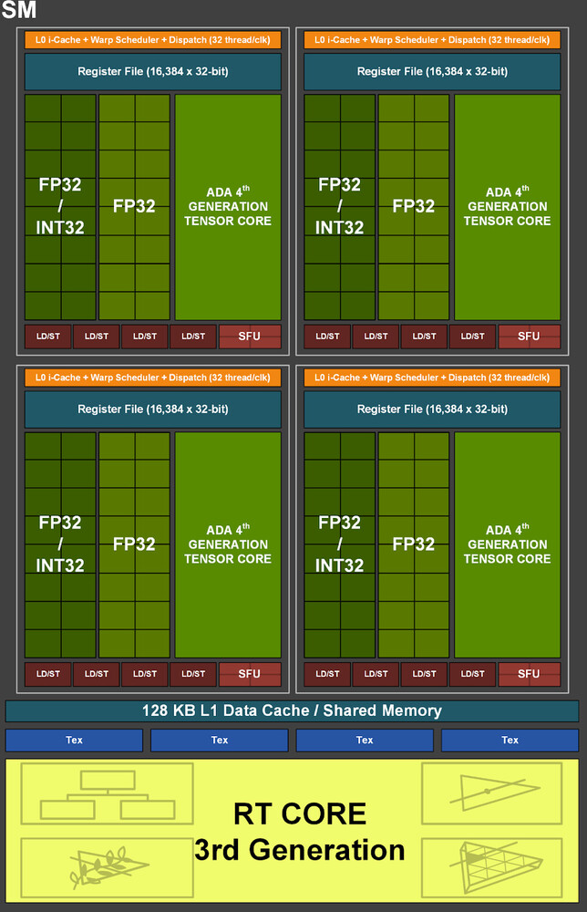
The Ada graphics architecture heralds the third generation of the NVIDIA RTX technology, an effort toward increasing the realism of game visuals by leveraging real-time ray tracing, without the enormous amount of compute power required to draw purely ray-traced 3D graphics. This is done by blending conventional raster graphics with ray traced elements such as reflections, lighting, and global illumination, to name a few. The 3rd generation of RTX introduces the new higher IPC "Ada" CUDA core, 3rd generation RT core, 4th generation Tensor core, and the new Optical Flow Processor, a component that plays a key role in generating new frames without involving the GPU's main graphics rendering pipeline.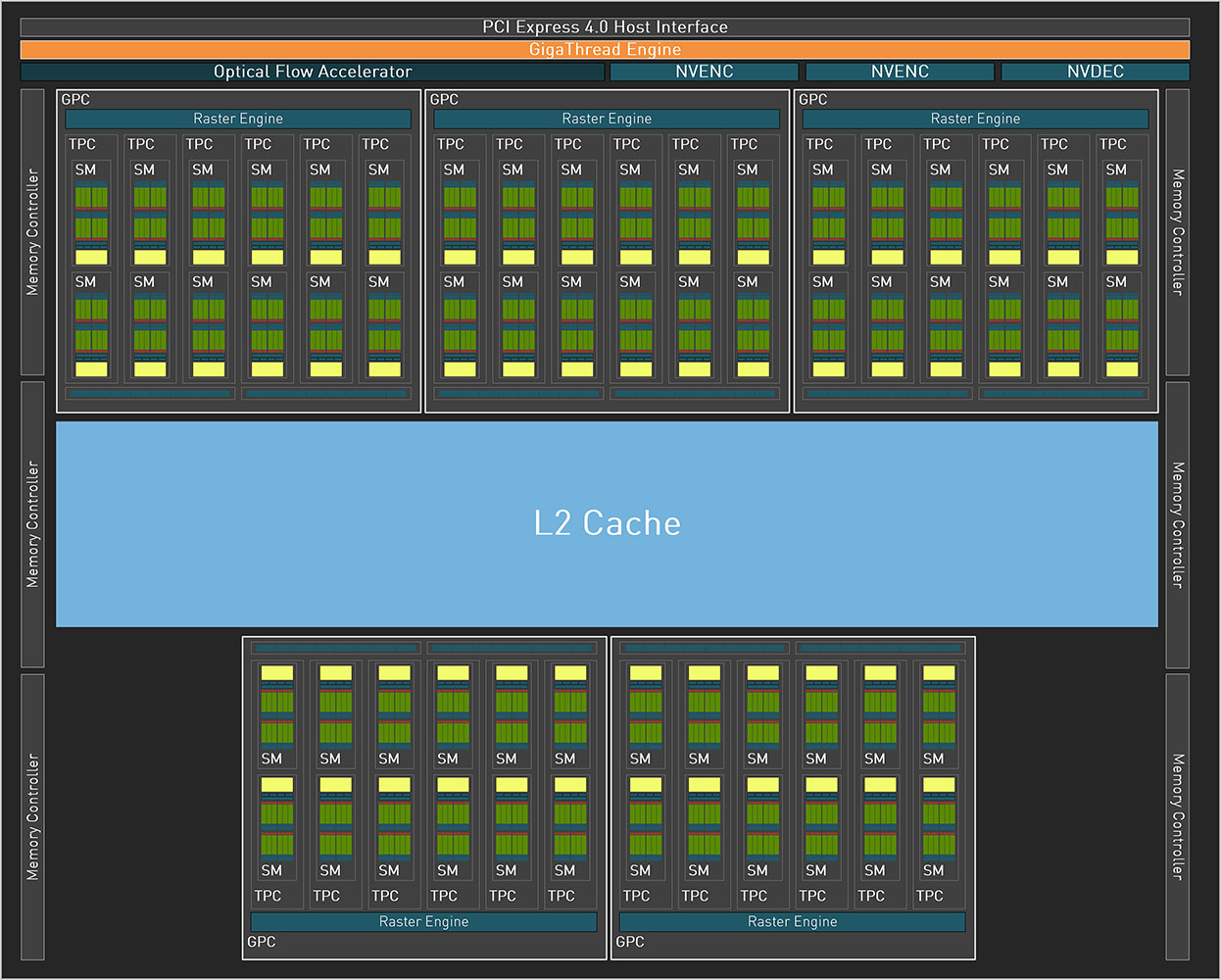
The GeForce Ada graphics architecture driving the RTX 4070 Ti leverages the TSMC 5 nm EUV foundry process to increase transistor counts. At the heart of this GPU is the new AD104 silicon, which has a fairly high transistor count of 35.8 billion, which is more than double that of the previous-generation GA104. The GPU features a PCI-Express 4.0 x16 host interface, and a 192-bit wide GDDR6X memory bus, which on the RTX 4070 Ti wires out to 12 GB of memory. The Optical Flow Accelerator (OFA) is an independent top-level component. The chip features two NVENC and one NVDEC units in the GeForce RTX 40-series, letting you run two independent video encoding streams (useful for game-streamers).
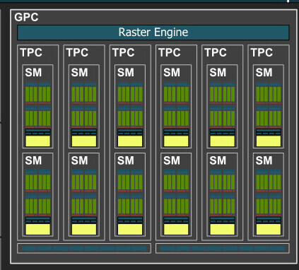
The essential component hierarchy is similar to past generations of NVIDIA GPUs. The AD104 silicon features 5 Graphics Processing Clusters (GPCs), each of these has all the SIMD and graphics rendering machinery, and is a small GPU in its own right. Each GPC shares a raster engine (geometry processing components) and two ROP partitions (each with eight ROP units). The GPC of the AD104 contains six Texture Processing Clusters (TPCs), the main number-crunching machinery. Each of these has two Streaming Multiprocessors (SM), and a Polymorph unit. Each SM contains 128 CUDA cores across four partitions. Half of these CUDA cores are pure-FP32; while the other half is capable of FP32 or INT32. The SM retains concurrent FP32+INT32 math processing capability. The SM also contains a 3rd generation RT core, four 4th generation Tensor cores, some cache memory, and four TMUs. There are 12 SM per GPC, so 1,536 CUDA cores, 48 Tensor cores, and 12 RT cores; per GPC. There are five such GPCs, which add up to 7,680 CUDA cores, 240 TMUs, 240 Tensor Cores, and 60 RT cores. Each GPC contributes 16 ROPs, so there are 80 ROPs on the silicon. The RTX 4070 Ti maxes out the AD104 silicon.
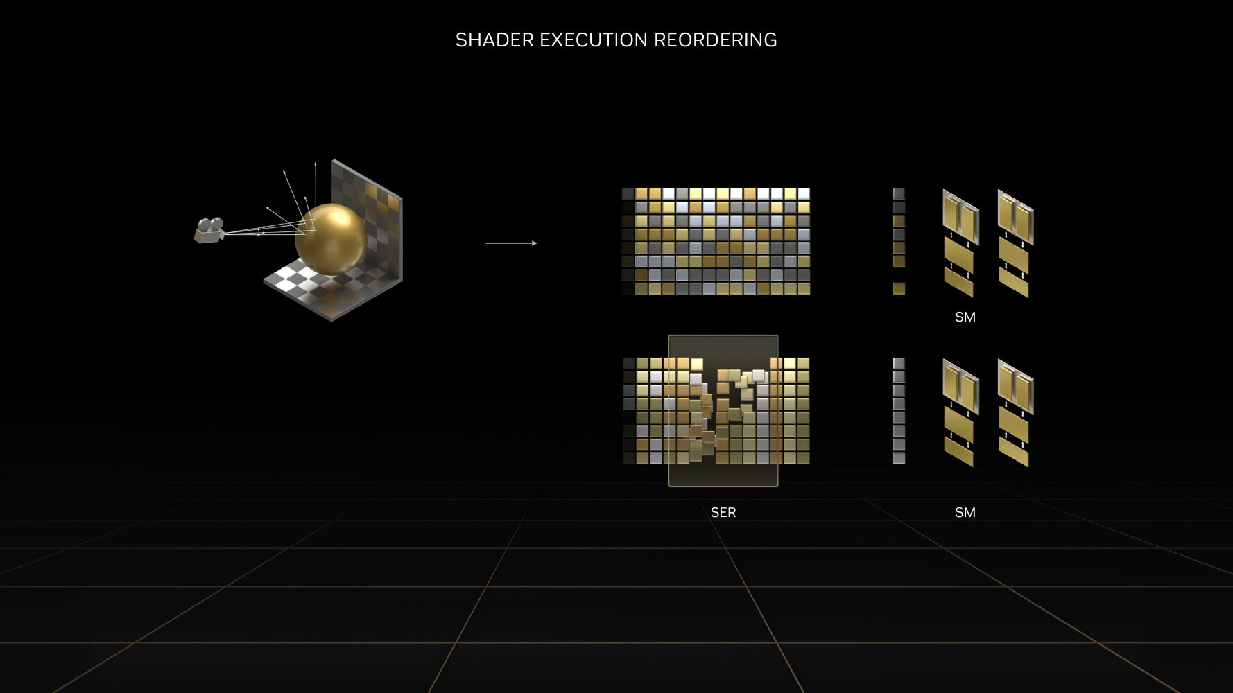
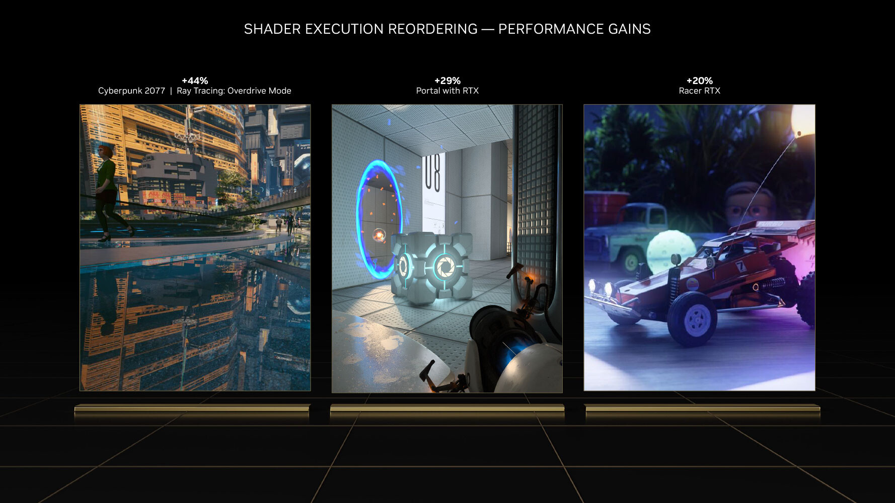
The 3rd generation RT core accelerates the most math-intensive aspects of real-time ray tracing, including BVH traversal. Displaced micro-mesh engine is a revolutionary feature introduced with the new 3rd generation RT core. Just as mesh shaders and tessellation have had a profound impact on improving performance with complex raster geometry, allowing game developers to significantly increase geometric complexity; DMMs is a method to reduce the complexity of the bounding-volume hierarchy (BVH) data-structure, which is used to determine where a ray hits geometry. Previously, the BVH had to capture even the smallest details to properly determine the intersection point. Ada's ray tracing architecture also receives a major performance uplift from Shader Execution Reordering (SER), a software-defined feature that requires awareness from game-engines, to help the GPU reorganize and optimize worker threads associated with ray tracing.
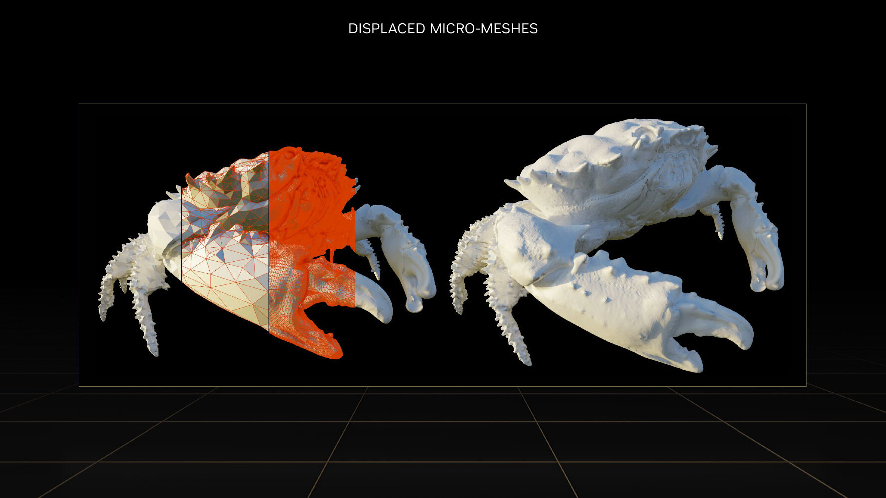
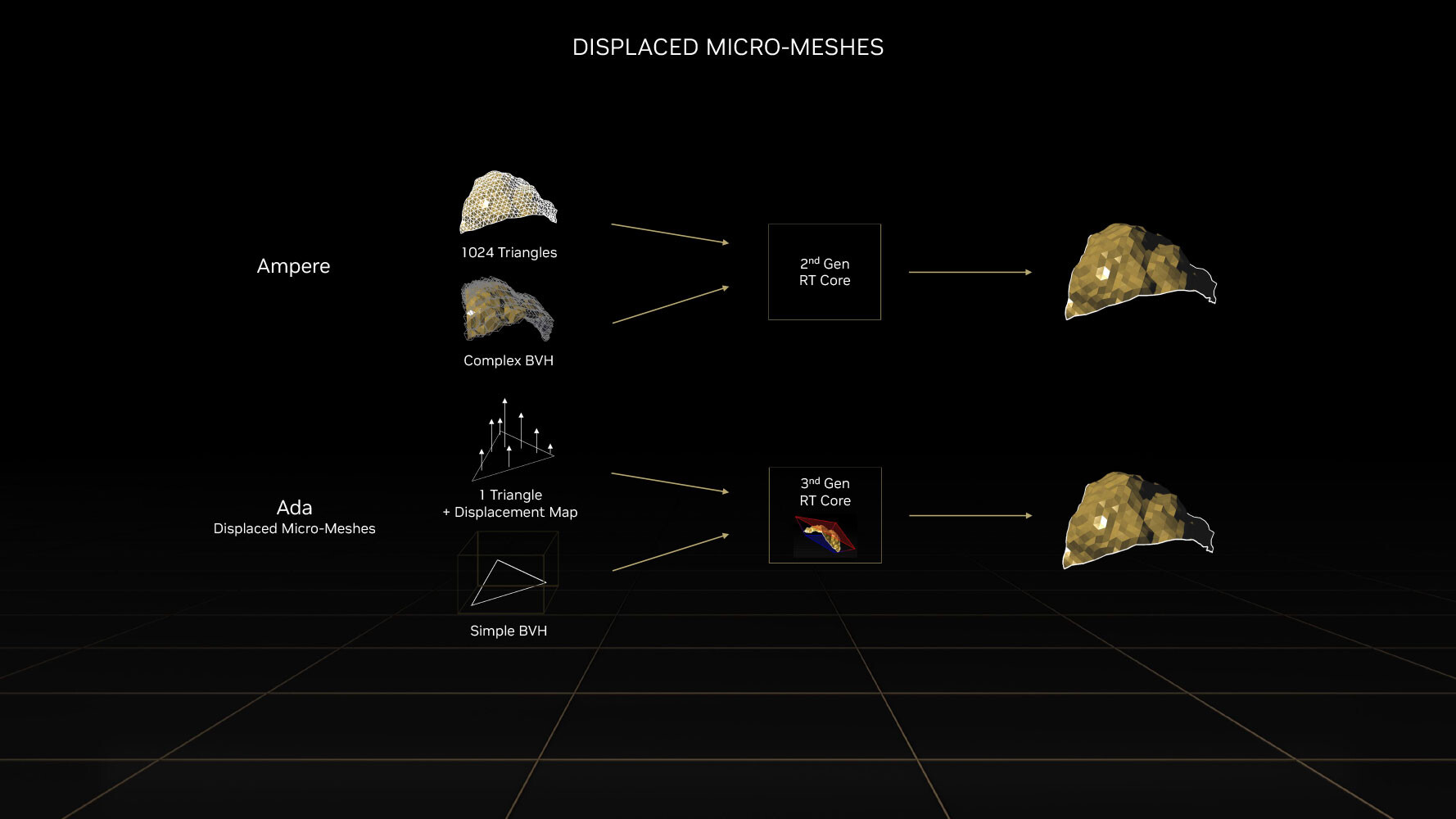
The BVH now needn't have data for every single triangle on an object, but can represent objects with complex geometry as a coarse mesh of base triangles, which greatly simplifies the BVH data structure. A simpler BVH means less memory consumed and helps to greatly reduce ray tracing CPU load, because the CPU only has to generate a smaller structure. With older "Ampere" and "Turing" RT cores, each triangle on an object had to be sampled at high overhead, so the RT core could precisely calculate ray intersection for each triangle. With Ada, the simpler BVH, plus the displacement maps can be sent to the RT core, which is now able to figure out the exact hit point on its own. NVIDIA has seen 11:1 to 28:1 compression in total triangle counts. This reduces BVH compile times by 7.6x to over 15x, in comparison to the older RT core; and reducing its storage footprint by anywhere between 6.5 to 20 times. DMMs could reduce disk- and memory bandwidth utilization, utilization of the PCIe bus, as well as reduce CPU utilization. NVIDIA worked with Simplygon and Adobe to add DMM support for their tool chains.

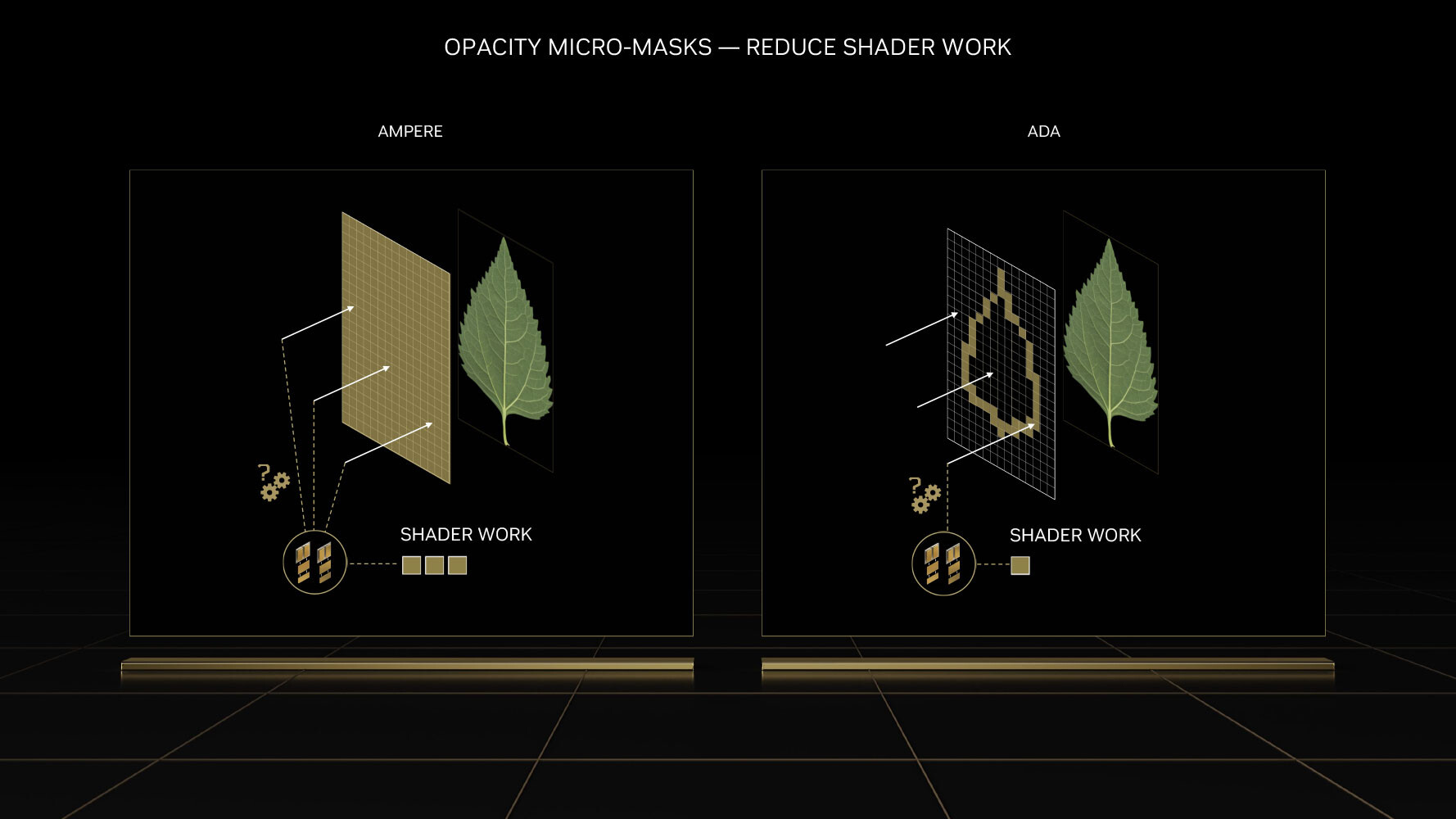
Opacity Micro Meshes (OMM) is a new feature introduced with Ada to improve rasterization performance, particularly with objects that have alpha (transparency data). Most low-priority objects in a 3D scene, such as leaves on a tree, are essentially rectangles with textures on the leaves where the transparency (alpha) creates the shape of the leaf. RT cores have a hard time intersecting rays with such objects, because they're not really in the shape that they appear (they're really just rectangles with textures that give you the illusion of shape). Previous-generation RT cores had to have multiple interactions with the rendering stage to figure out the shape of a transparent object, because they couldn't test for alpha by themselves.
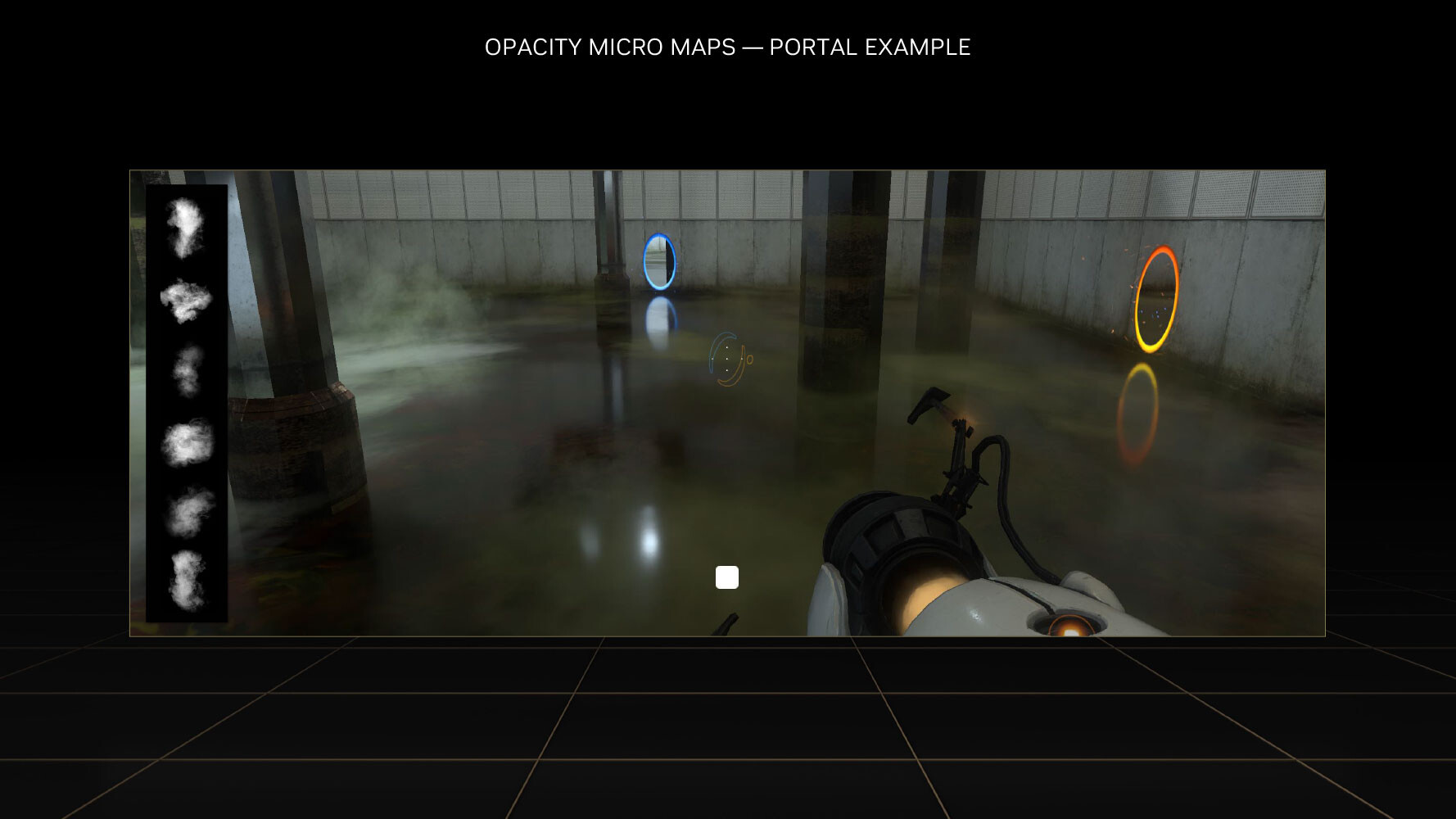
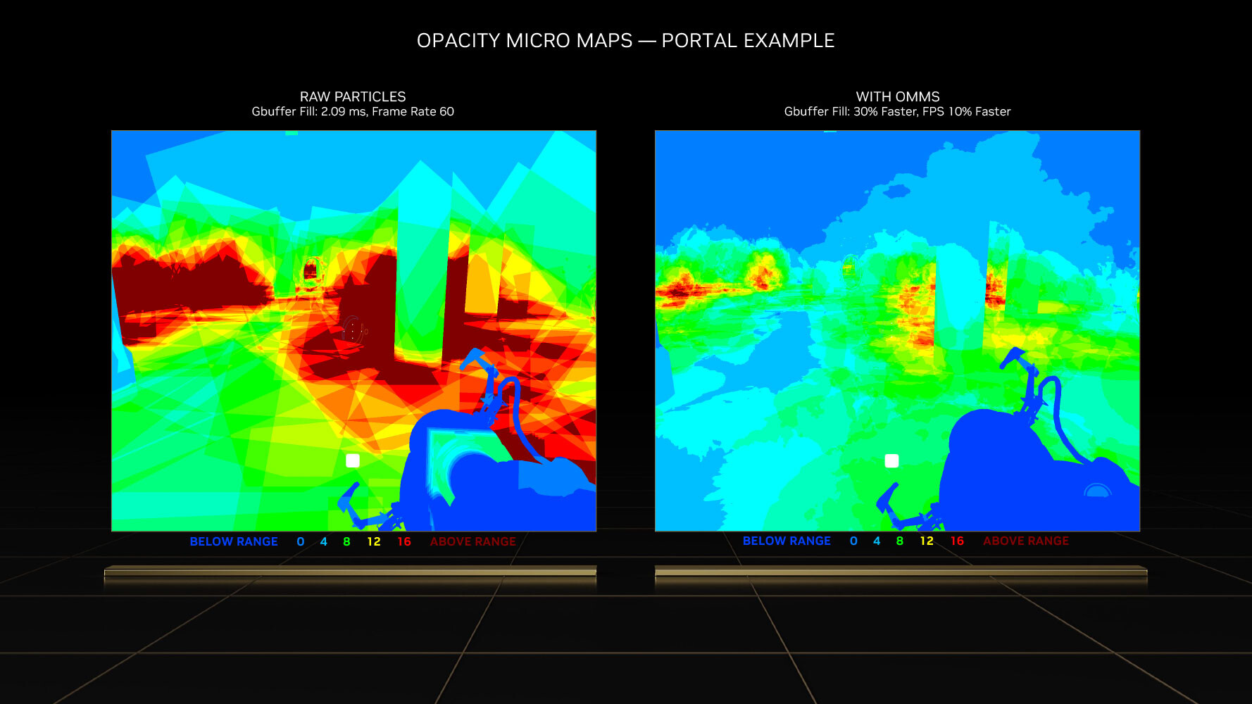
This has been solved by using OMMs. Just as DMMs simplify geometry by creating meshes of micro-triangles; OMMs create meshes of rectangular textures that align with parts of the texture that aren't alpha, so the RT core has a better understanding of the geometry of the object, and can correctly calculate ray intersections. This has a significant performance impact on shading performance in non-RT applications, too. Practical applications of OMMs aren't just low-priority objects such as vegetation, but also smoke-sprites and localized fog. Traditionally there was a lot of overdraw for such effects, because they layered multiple textures on top of each other, that all had to be fully processed by the shaders. Now only the non-opaque pixels get executed—OMMs provide a 30 percent speedup with graphics buffer fill-rates, and a 10 percent impact on frame-rates.
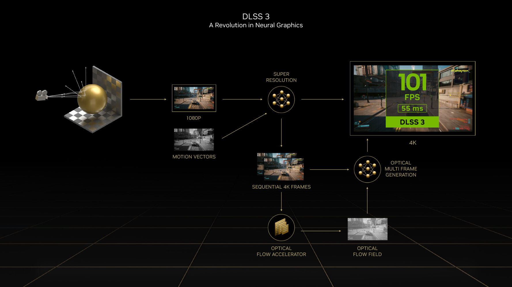
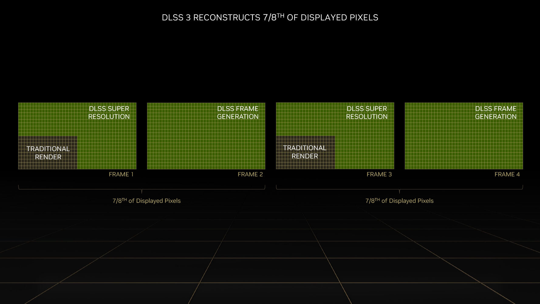
DLSS 3 introduces a revolutionary new feature that promises a doubling in frame-rate at comparable quality, it's called AI frame-generation. While it has all the features of DLSS 2 and its AI super-resolution (scaling up a lower-resolution frame to native resolution with minimal quality loss); DLSS 3 can generate entire frames simply using AI, without involving the graphics rendering pipeline. Later in the article, we will show you DLSS 3 in action.
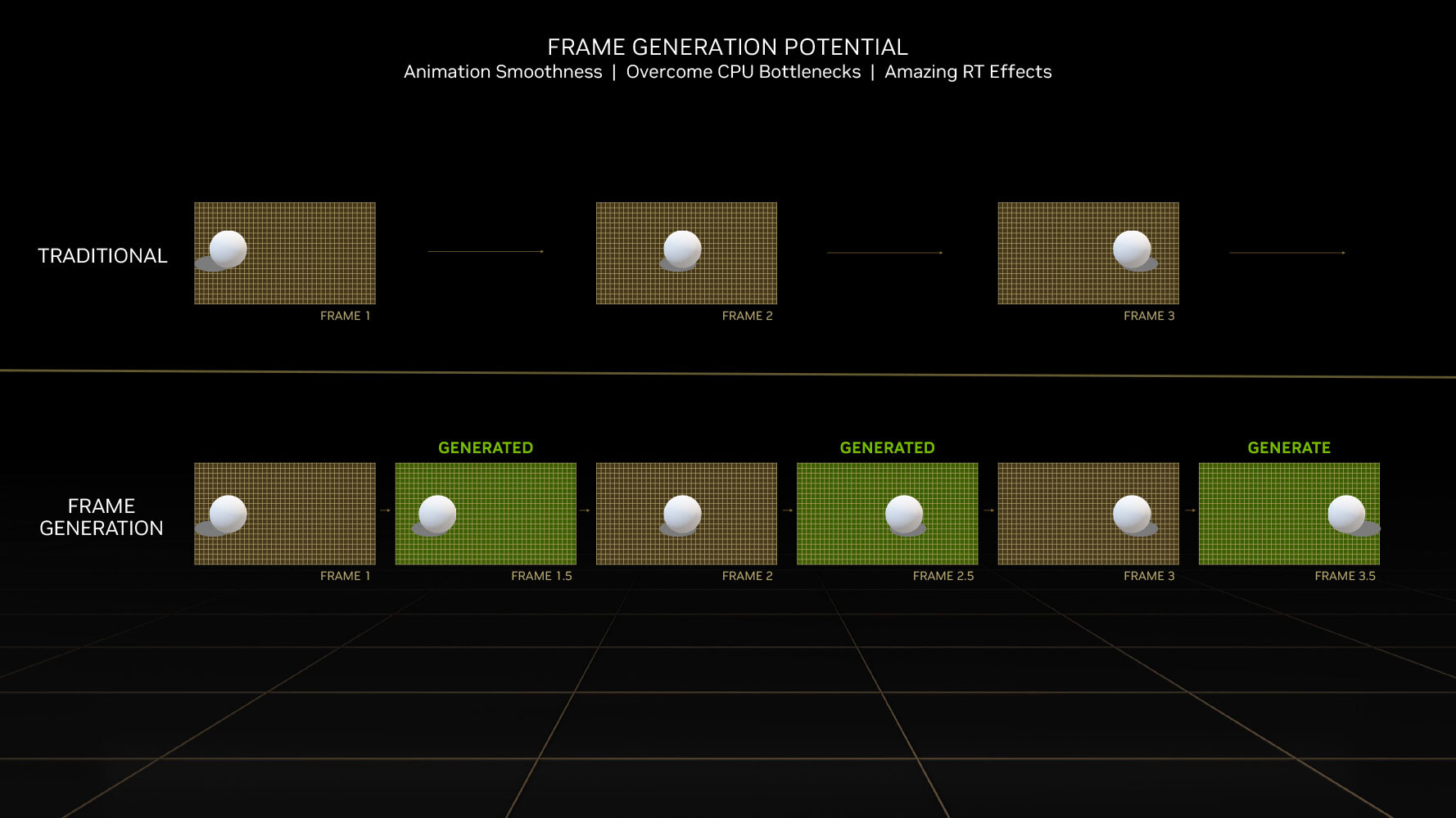

Every alternating frame with DLSS 3 is hence AI-generated, without being a replica of the previous rendered frame. This is possible only on the Ada graphics architecture, because of a hardware component called the optical flow accelerator (OFA), which assists in predicting what the next frame could look like, by creating what NVIDIA calls an optical flow-field. OFA ensures that the DLSS 3 algorithm isn't confused by static objects in a rapidly-changing 3D scene (such as a race sim). The process heavily relies on the performance uplift introduced by the FP8 math format of the 4th generation Tensor core. A third key ingredient of DLSS 3 is Reflex. By reducing the rendering queue to zero, Reflex plays a vital role in ensuring that frame-times with DLSS 3 are at an acceptable level, and a render-queue doesn't confuse the upscaler. A combination of OFA and the 4th Gen Tensor core is why the Ada architecture is required to use DLSS 3, and why it won't work on older architectures.
Packaging


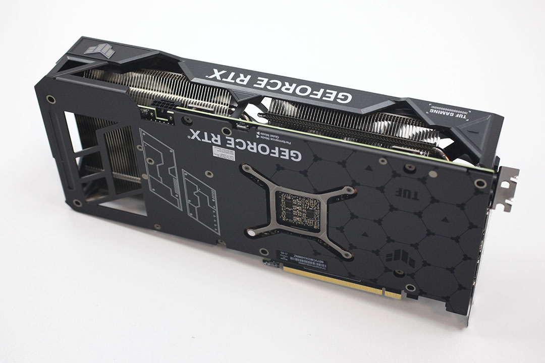
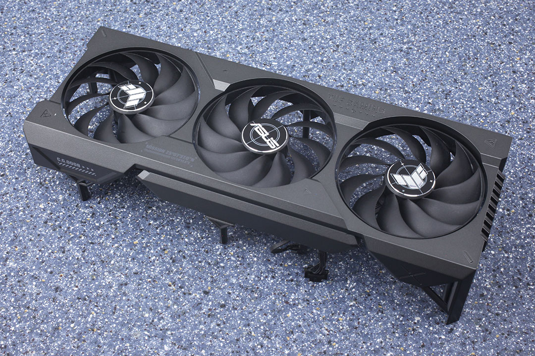
The Card


The TUF RTX 4070 Ti follows the company's GeForce 40 design theme—a bulky look, with surfaces in various metal colors. On the back you get a thick metal backplate with cutouts for airflow.
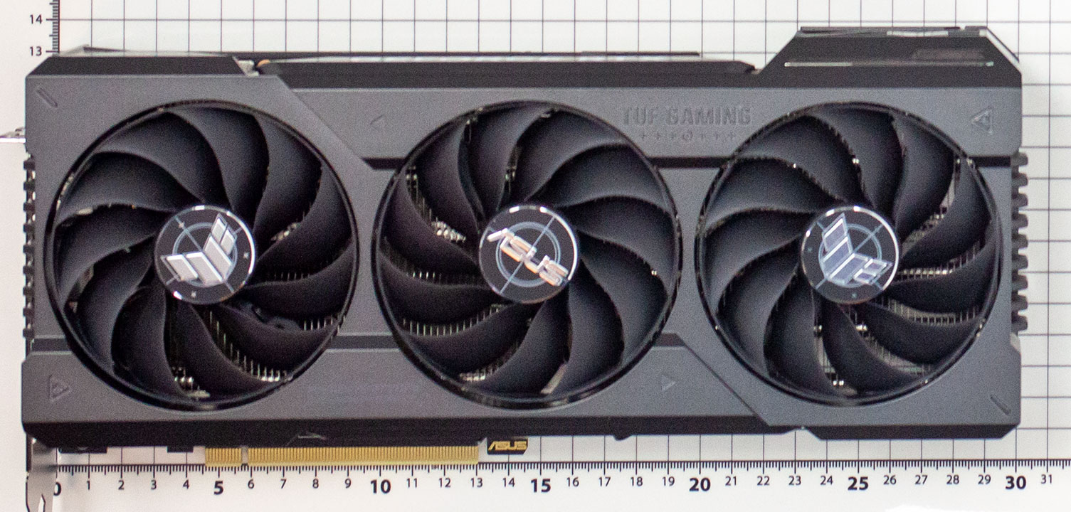
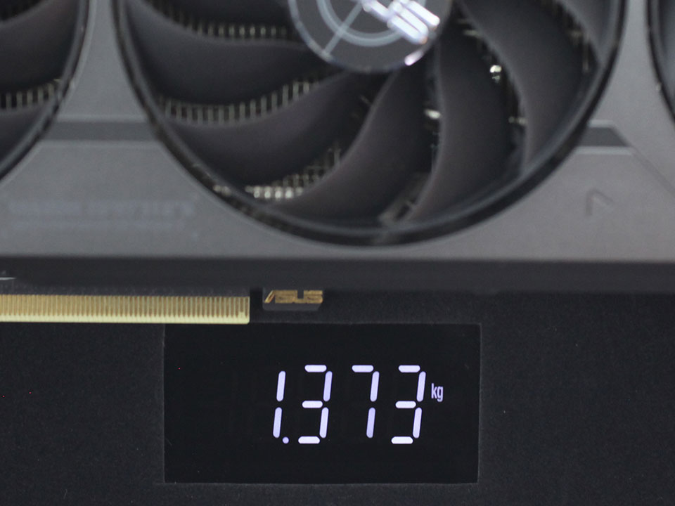
Dimensions of the card are 30.0 x 14.0 cm, and it weighs 1373 g.
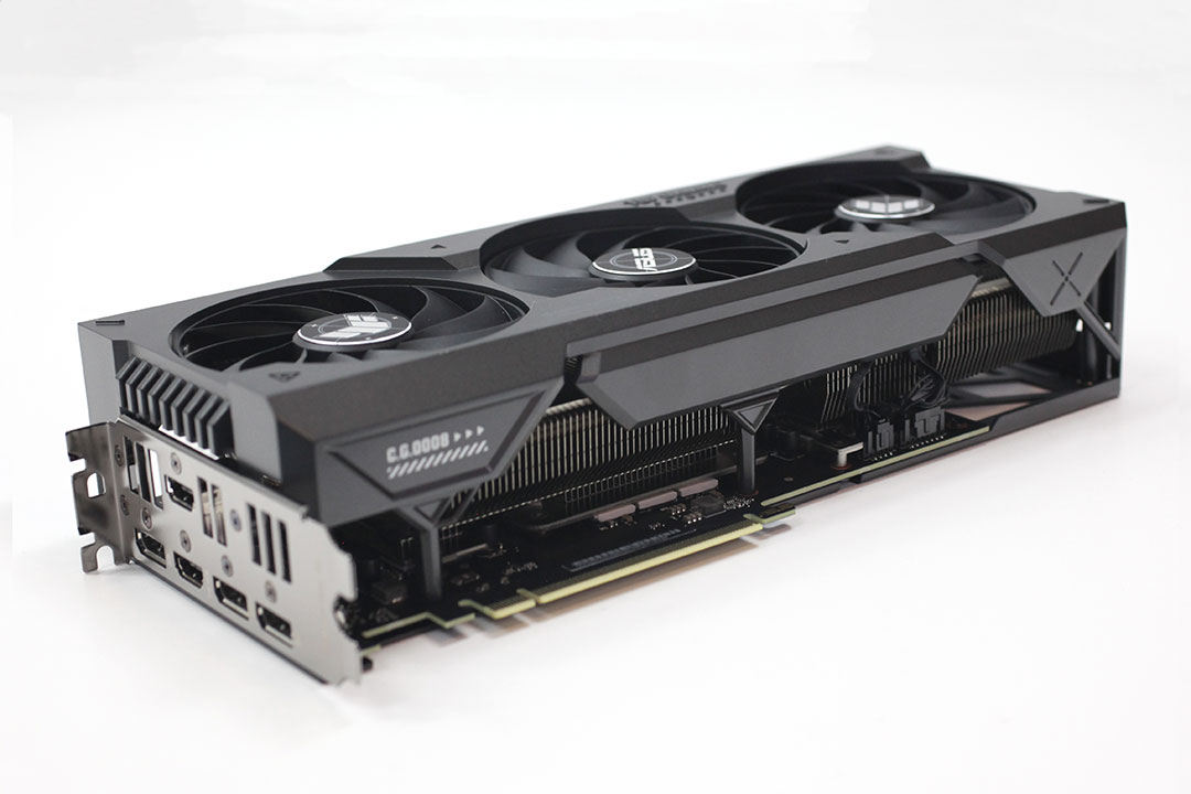
Installation requires three slots in your system.
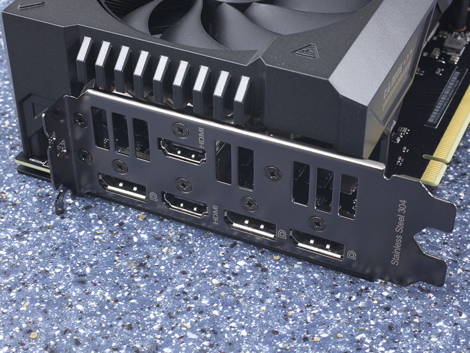
Display connectivity includes three standard DisplayPort 1.4a ports and two HDMI 2.1a (same as Ampere).
NVIDIA introduces the concept of dual NVDEC and NVENC Codecs with the Ada architecture. This means there are now two independent sets of hardware-accelerators; so you can encode and decode two streams of video in parallel, or one stream at double the FPS rate. The new 8th Gen NVENC now accelerates AV1 encoding, besides HEVC. You also get an "optical flow accelerator" unit that is able to calculate intermediate frames for videos, to smooth playback. The same hardware unit is used for frame generation in DLSS 3.
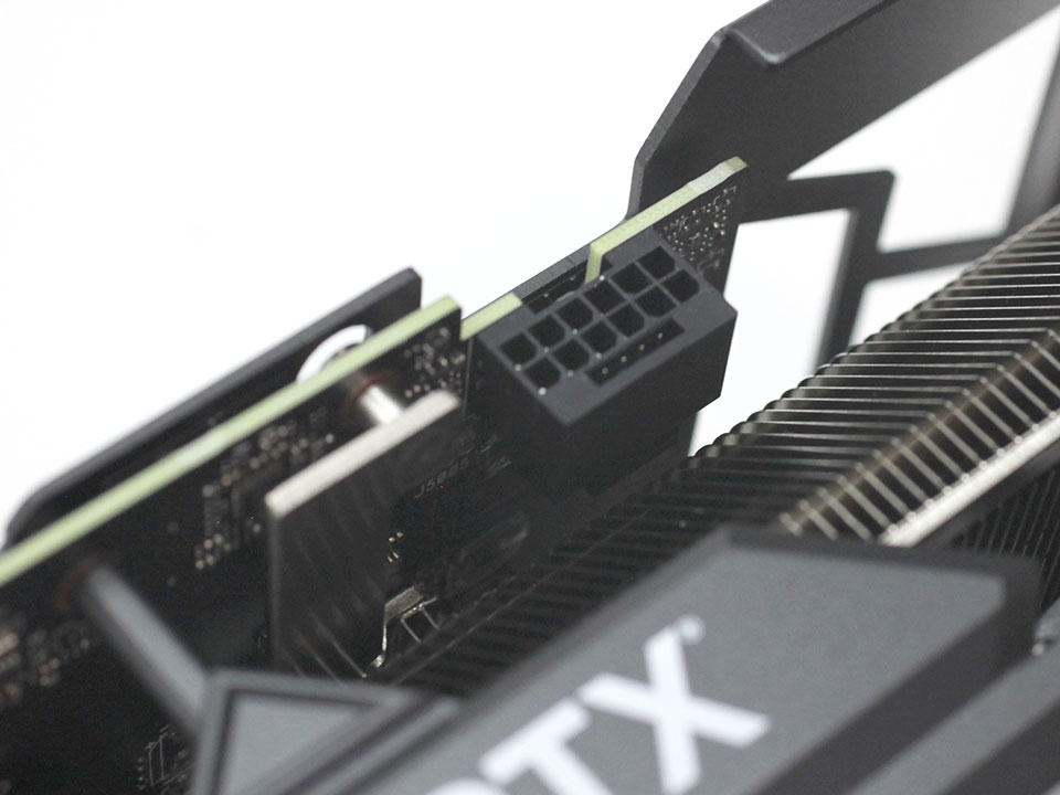
The card uses the new 12+4 pin ATX 12VHPWR connector, which is rated for up to 600 W of power draw. An adapter cable from 2x PCIe 8-pin is included. Of course the 4x 8-pin to 16-pin adapter cables from RTX 4090 will also work with the RTX 4070 Ti.

This dual BIOS switch lets you toggle from the default "performance" BIOS, to the "quiet" mode BIOS.
Teardown
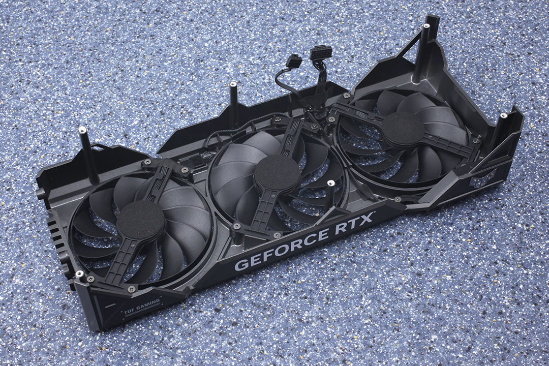
The fan assembly can be replaced easily, it's just a few screws to take off.

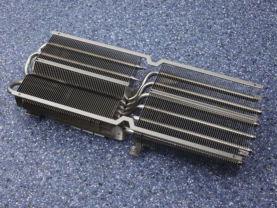
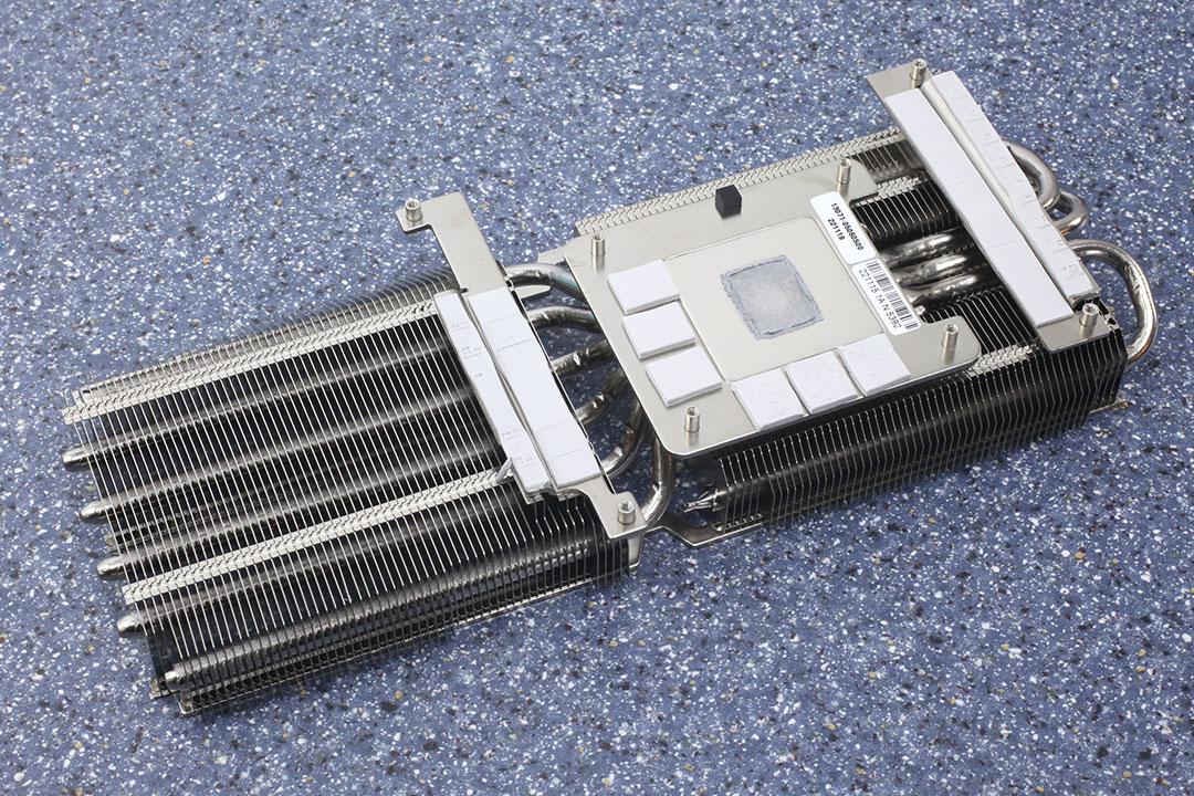
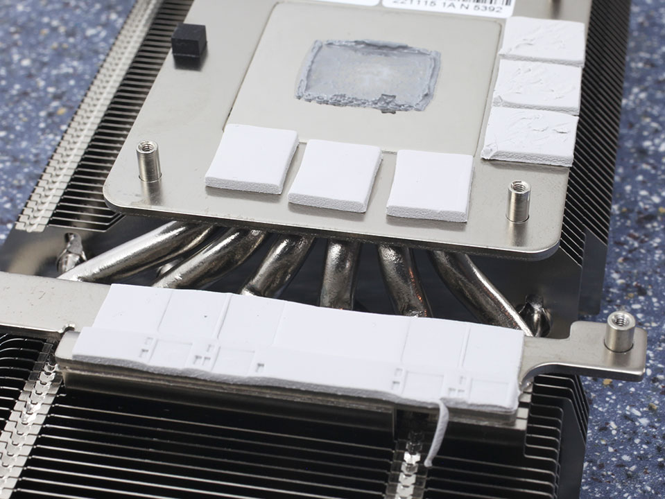
The heatsink provides cooling for the GPU, memory chips and VRM circuitry. ASUS has installed six heatpipes.
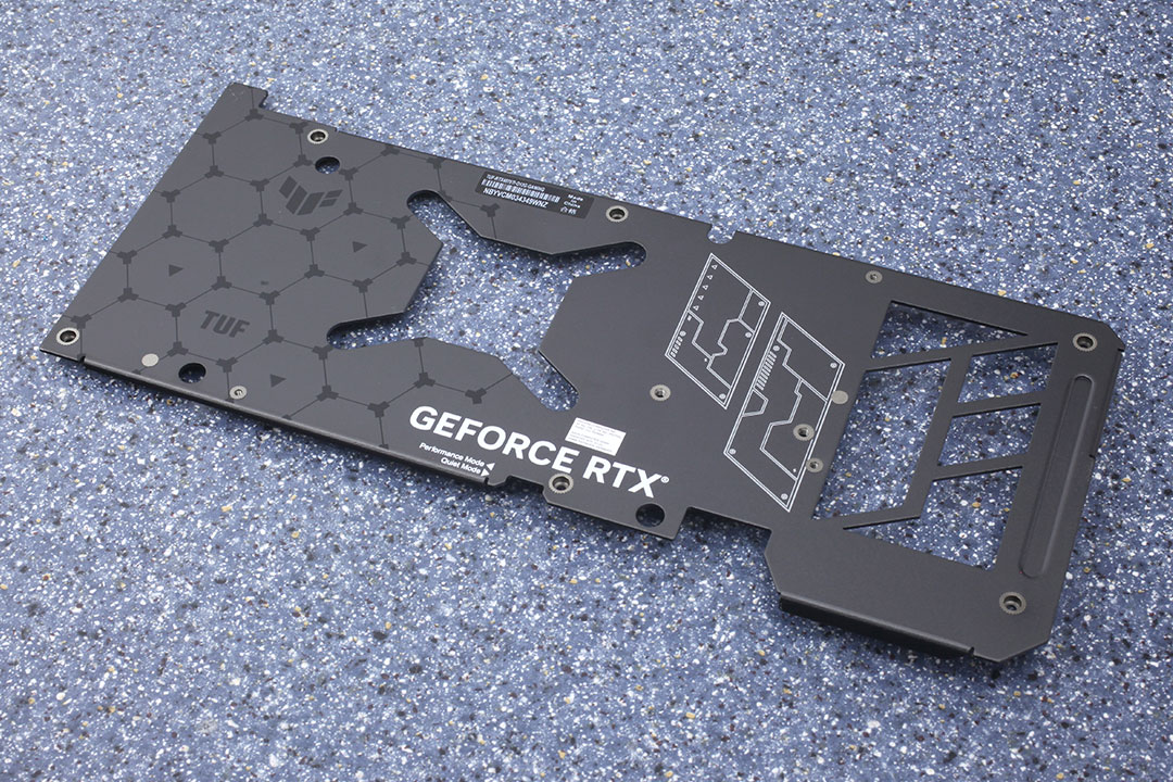

The backplate is made from metal, it protects the card against damage during installation and handling.
High-resolution PCB Pictures
These pictures are for the convenience of volt modders and people who would like to see all the finer details on the PCB. Feel free to link back to us and use these in your articles, videos or forum posts.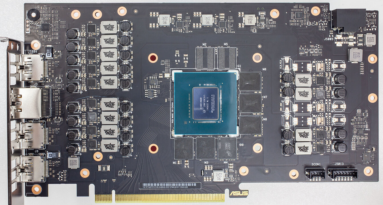

High-resolution versions are also available (front, back).
Our Patreon Silver Supporters can read articles in single-page format.
Apr 18th, 2025 03:23 EDT
change timezone
Latest GPU Drivers
New Forum Posts
- RX 9000 series GPU Owners Club (373)
- It's happening again, melting 12v high pwr connectors (1024)
- D5400XS Skulltrail (1)
- Help For XFX RX 590 GME Chinese - Vbios (8)
- Random Entire System Stutter when using Throttlestop (7)
- Help needed OC on Intel 285k (3)
- 3090 zotac Trinity Oc dead or psu weak? (39)
- RTX5000 Series Owners Club (181)
- random system shutdown with fans running at full speed (41)
- What's your latest tech purchase? (23566)
Popular Reviews
- ASUS GeForce RTX 5060 Ti TUF OC 16 GB Review
- NVIDIA GeForce RTX 5060 Ti PCI-Express x8 Scaling
- G.SKILL Trident Z5 NEO RGB DDR5-6000 32 GB CL26 Review - AMD EXPO
- Palit GeForce RTX 5060 Ti Infinity 3 16 GB Review
- ASUS GeForce RTX 5060 Ti Prime OC 16 GB Review
- Zotac GeForce RTX 5060 Ti AMP 16 GB Review
- MSI GeForce RTX 5060 Ti Gaming OC 16 GB Review
- MSI GeForce RTX 5060 Ti Gaming Trio OC 16 GB Review
- ASUS GeForce RTX 5080 TUF OC Review
- Teevolution Terra Pro Review
Controversial News Posts
- NVIDIA GeForce RTX 5060 Ti 16 GB SKU Likely Launching at $499, According to Supply Chain Leak (182)
- NVIDIA Sends MSRP Numbers to Partners: GeForce RTX 5060 Ti 8 GB at $379, RTX 5060 Ti 16 GB at $429 (127)
- Nintendo Confirms That Switch 2 Joy-Cons Will Not Utilize Hall Effect Stick Technology (105)
- Over 200,000 Sold Radeon RX 9070 and RX 9070 XT GPUs? AMD Says No Number was Given (100)
- Nintendo Switch 2 Launches June 5 at $449.99 with New Hardware and Games (99)
- NVIDIA Launches GeForce RTX 5060 Series, Beginning with RTX 5060 Ti This Week (96)
- Sony Increases the PS5 Pricing in EMEA and ANZ by Around 25 Percent (85)
- NVIDIA PhysX and Flow Made Fully Open-Source (77)