 125
125
ASUS GeForce RTX 5060 Ti TUF OC 16 GB Review
(125 Comments) »Introduction
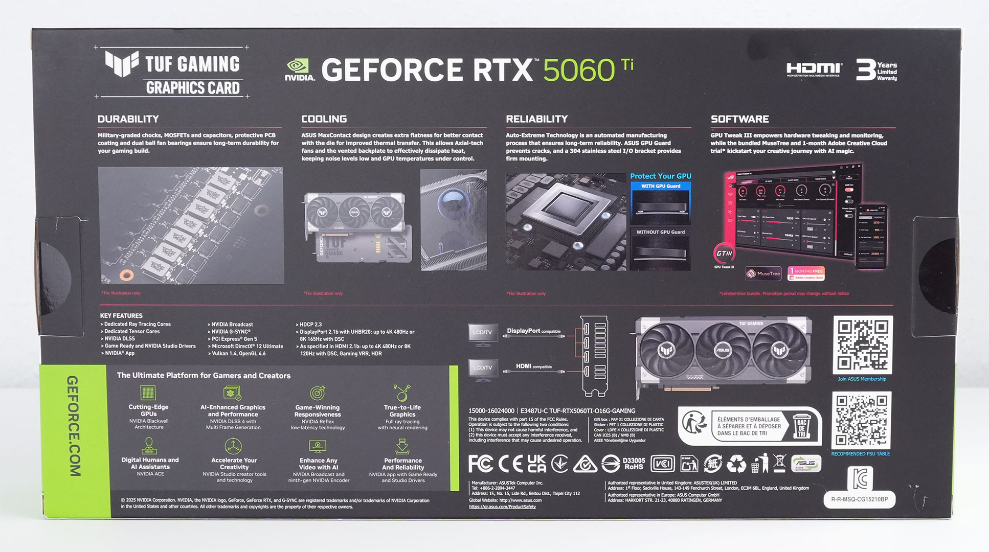
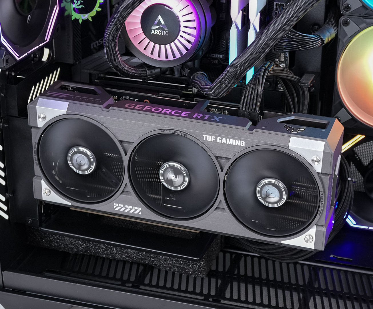
ASUS TUF Gaming GeForce RTX 5060 Ti OC 16 GB is the company's premium custom-design rendition of NVIDIA's new performance segment GPU making its debut today. The card sports the latest generation of TUF Gaming board design by ASUS, particularly its Vented Exoskeleton architecture that relies on a heavy aluminium fin-stack heatsink, with a cooler shroud that exposes most of this heatsink externally, for better ventilation. The card also offers the company's latest Axial-Tech fans with double ball bearings. Other premium touches include a modern 16-pin 12V-2x6 power connector, and dual-BIOS.

The new GeForce RTX 5060 Ti comes in two memory variants, both of which are launching today. In this review, we take a close look at a 16 GB card. Both memory variants otherwise come with identical specs. The RTX 5060 Ti is recommended by NVIDIA for maxed out gameplay at 1080p, including with ray tracing, although we believe the RTX 5060 Ti occupies a gray area between what constitutes mid-range, and performance segment; and although this is marketed as a 1080p-class GPU, it should still be capable of 1440p, with fairly high settings and ray tracing. You just need to know your way around your game's settings, or let the NVIDIA App pick the best settings for you. Better yet, unlock the awesome capabilities of DLSS 4 and Multi Frame Generation to transform your playability.
The GeForce RTX 5060 Ti is the fifth GPU from the RTX 50-series Blackwell generation. The new Blackwell graphics architecture introduces Neural Rendering—the ability for the GPU to run generative AI models that create in-game assets in real time, and combine them with raster 3D graphics. This is made possible with a new hardware scheduler on the silicon, called the AI Management Processor (AMP). The API-level groundwork for Neural Rendering has been laid by NVIDIA and Microsoft, letting 3D apps directly address the Tensor cores on the GPU.
The GeForce Blackwell generation also introduces DLSS 4 and Multi Frame Generation. DLSS 4 introduces updated Transformer-based AI models replacing the older CNN-based ones, which improve image quality for super resolution, at every performance preset. These Transformer models also power ray reconstruction and frame generation. Multi Frame Generation is the ability for the GPU to generate up to three frames following a conventionally rendered frame completely using AI, effectively quadrupling frame rates. This should come in handy with high refresh-rate displays where a playable frame rate above 40 FPS is transformed into something in excess of 100 FPS, to keep pace with the refresh rate of the display. Multi Frame Generation is exclusive to Blackwell as it relies on hardware flip-metering, a component that's part of Blackwell's display engine.
The GeForce RTX 5060 Ti introduces the new GB206 silicon, NVIDIA's fourth new gaming GPU based on this architecture. The RTX 5060 Ti maxes out the GB206, enabling all 36 SM (streaming multiprocessors) present on the silicon, which works out to 4,608 CUDA cores, 144 Tensor cores, 36 RT cores, and 144 TMUs. The silicon comes with 48 ROPs, and 32 MB of L2 cache. The memory interface for both the 8 GB and 16 GB variants is 128-bit wide, but this is the updated GDDR7 memory type. For the RTX 5060 Ti, which uses 28 Gbps GDDR7 memory chips, this means a much-needed 55% increase in memory bandwidth over the previous RTX 4060 Ti that uses 18 Gbps GDDR6.
The ASUS TUF Gaming RTX 5060 Ti OC 16 GB offers factory overclocked speeds of 2662 MHz over the 2572 MHz reference speeds, with its default P-BIOS (OC BIOS). The Q-BIOS (quiet BIOS) scales down clock speeds to favor a tighter fan curve that keeps noise levels down when gaming. ASUS is among many partner cards we're reviewing today to implement a 16-pin 12V-2x6 power connector. The RTX 5060 Ti comes with a TGP of 180 W, which should normally work just fine with a single 8-pin PCIe power connector, as was the case with the RTX 4070. ASUS includes an adapter that converts two 8-pin to a 16-pin, which means the card is able to meet all its power budget from the power connector. ASUS is pricing the TUF Gaming RTX 5060 Ti OC 16 GB at $600, a massive step up from the $425 MSRP.
| Price | Cores | ROPs | Core Clock | Boost Clock | Memory Clock | GPU | Transistors | Memory | |
|---|---|---|---|---|---|---|---|---|---|
| RX 7600 | $250 | 2048 | 64 | 2250 MHz | 2625 MHz | 2250 MHz | Navi 33 | 13300M | 8 GB, GDDR6, 128-bit |
| Arc B570 | $220 | 2304 | 80 | 2500 MHz | N/A | 2375 MHz | BMG-G21 | 19600M | 10 GB, GDDR6, 160-bit |
| RX 7600 XT | $400 | 2048 | 64 | 2470 MHz | 2755 MHz | 2250 MHz | Navi 33 | 13300M | 16 GB, GDDR6, 128-bit |
| RTX 4060 | $270 | 3072 | 48 | 1830 MHz | 2460 MHz | 2125 MHz | AD107 | 18900M | 8 GB, GDDR6, 128-bit |
| Arc A770 | $250 | 4096 | 128 | 2100 MHz | N/A | 2187 MHz | ACM-G10 | 21700M | 16 GB, GDDR6, 256-bit |
| Arc B580 | $250 | 2560 | 80 | 2670 MHz | N/A | 2375 MHz | BMG-G21 | 19600M | 12 GB, GDDR6, 192-bit |
| RTX 4060 Ti | $380 | 4352 | 48 | 2310 MHz | 2535 MHz | 2250 MHz | AD106 | 22900M | 8 GB, GDDR6, 128-bit |
| RX 7700 XT | $450 | 3456 | 96 | 2171 MHz | 2544 MHz | 2250 MHz | Navi 32 | 26500M | 12 GB, GDDR6, 192-bit |
| RTX 5060 Ti | $380 | 4608 | 48 | 2407 MHz | 2572 MHz | 1750 MHz | GB206 | 21900M | 8 GB, GDDR7, 128-bit |
| RTX 5060 Ti 16 GB | $430 | 4608 | 48 | 2407 MHz | 2572 MHz | 1750 MHz | GB206 | 21900M | 16 GB, GDDR7, 128-bit |
| ASUS RTX 5060 Ti 16 GB TUF OC | $600 | 4608 | 48 | 2407 MHz | 2662 MHz | 1750 MHz | GB206 | 21900M | 16 GB, GDDR7, 128-bit |
| RTX 4070 | $400 | 5888 | 64 | 1920 MHz | 2475 MHz | 1313 MHz | AD104 | 35800M | 12 GB, GDDR6X, 192-bit |
| RX 7800 XT | $540 | 3840 | 96 | 2124 MHz | 2430 MHz | 2425 MHz | Navi 32 | 28100M | 16 GB, GDDR6, 256-bit |
| RTX 4070 Super | $600 | 7168 | 80 | 1980 MHz | 2475 MHz | 1313 MHz | AD104 | 35800M | 12 GB, GDDR6X, 192-bit |
| RX 7900 GRE | $650 | 5120 | 160 | 1880 MHz | 2245 MHz | 2250 MHz | Navi 31 | 57700M | 16 GB, GDDR6, 256-bit |
| RTX 4070 Ti | $700 | 7680 | 80 | 2310 MHz | 2610 MHz | 1313 MHz | AD104 | 35800M | 12 GB, GDDR6X, 192-bit |
| RTX 5070 | $600 | 6144 | 80 | 2325 MHz | 2512 MHz | 1750 MHz | GB205 | 31100M | 12 GB, GDDR7, 192-bit |
| RTX 4070 Ti Super | $860 | 8448 | 96 | 2340 MHz | 2610 MHz | 1313 MHz | AD103 | 45900M | 16 GB, GDDR6X, 256-bit |
| RX 7900 XT | $720 | 5376 | 192 | 2000 MHz | 2400 MHz | 2500 MHz | Navi 31 | 57700M | 20 GB, GDDR6, 320-bit |
| RX 9070 | $625 | 3584 | 128 | 2070 MHz | 2520 MHz | 2518 MHz | Navi 48 | 53900M | 16 GB, GDDR6, 256-bit |
NVIDIA Blackwell Architecture

NVIDIA does not provide a block diagram for the GB206 GPU (we asked), so we had to quickly hack one out from the GB202 diagram. This is accurate just not as pretty.
The GeForce Blackwell graphics architecture heralds NVIDIA's 4th generation of RTX, the late-2010s re-invention of the modern GPU that sees a fusion of real time ray traced objects with conventional raster 3D graphics. With Blackwell, NVIDIA is helping add another dimension, neural rendering, the ability for the GPU to leverage a generative AI to create portions of a frame. This is different from DLSS, where an AI model is used to reconstruct details in an upscaled frame based on its training date, temporal frames, and motion vectors. Today we are reviewing NVIDIA's fifth GPU from this generation, the RTX 5060 Ti. At the heart of this graphics card is the new GB206 silicon. This chip has a unique die-size and SM count that doesn't have a predecessor from the previous Ada generation. With the GeForce Blackwell generation, NVIDIA tailored the SM counts of its GPUs closer to those of the actual SKUs, to minimize wasted die-space. The GB206 is maxed out by the RTX 5060 Ti. This is NVIDIA's fourth gaming GPU based on this architecture. It is built on the same NVIDIA 4N foundry node as the previous generation AD106. It is a tiny, somewhat square die measuring 181 mm², with a transistor count of 21.9 billion.
The GB206 silicon is laid out essentially in the same component hierarchy as past generations of NVIDIA GPUs, but with a few notable changes. The GPU features a PCI-Express 5.0 x8 host interface. PCIe Gen 5 has been around since Intel's 12th Gen Core "Alder Lake" and AMD's Ryzen 7000 "Zen 4," so there is a sizable install-base of systems that can take advantage of it. The GPU is of course compatible with older generations of PCIe. The GB206 also features the new GDDR7 memory interface that's making its debut with this generation. The chip features a 128-bit wide memory bus. NVIDIA is using this to drive 16 GB of memory at 28 Gbps speeds, yielding 448 GB/s of memory bandwidth, which is a 55% increase over the RTX 4060 Ti and its 18 Gbps GDDR6.
The GigaThread Engine is the main graphics rendering workload allocation logic on the GB206, but there's a new addition, a dedicated serial processor for managing all AI acceleration resources on the GPU, NVIDIA calls this AMP (AI management processor). Other components at the global level are the Optical Flow Processor, a component involved in older versions of DLSS frame generation and for video encoding; and an updated media acceleration engine consisting of one each of NVDEC and NVENC video accelerators. The new 9th Gen NVENC video encode accelerators come with 4:2:2 AV1 and HEVC encoding support. The central region of the GPU has the single largest common component, the 32 MB L2 cache, which the RTX 5060 Ti maxes out.
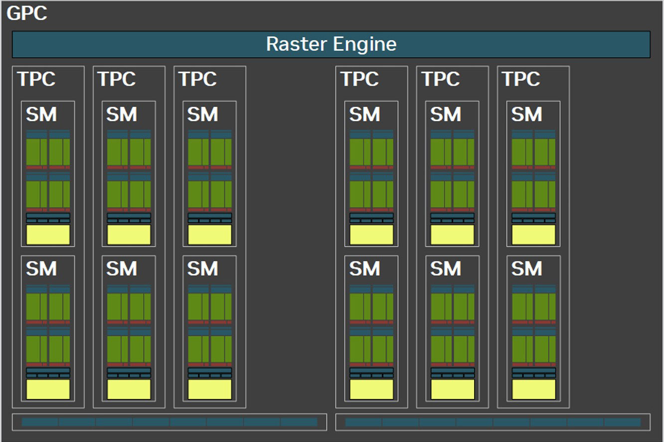
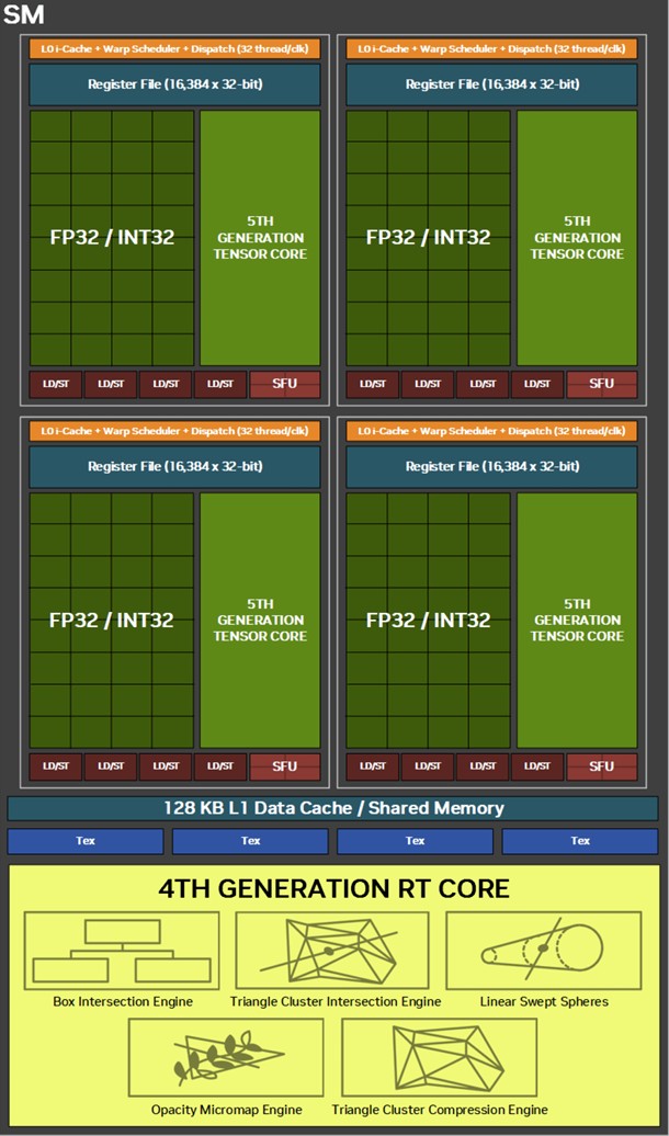

There are three graphics processing clusters (GPC) on the GB206. Each of these contains 12 streaming multiprocessors (SM) across 6 texture processing clusters (TPCs), resulting in 36 SM. Every GPC also contains a ROP partition with 12 ROPs, each, working out to 48 ROPs on the silicon. Within each SM, you'll find 128 CUDA cores. Unlike the Ada generation SM that each had 64 FP32+INT32 and 64 purely-FP32 SIMD units, the new Blackwell generation SM features concurrent FP32+INT32 capability on all 128 SIMD units. These 128 CUDA cores are arranged in four slices, each with a register file, a level-0 instruction cache, a warp scheduler, two sets of load-store units, and a special function unit (SFU) handling some special math functions such as trigonometry, exponents, logarithms, reciprocals, and square-root. The four slices share a 128 KB L1 data cache, and four TMUs. The most exotic components of the Blackwell SM are the four 5th Gen Tensor cores, and a 4th Gen RT core.
With 3 GPCs containing 6 TPCs each, there are a total of 36 SM, worth 4,160 CUDA cores, 144 Tensor cores, 36 RT cores, and 144 TMUs, on the GB206 silicon. The GB206 silicon is endowed with 48 ROPs, all of which are enabled on the RTX 5060 Ti. The RTX 5060 Ti also maxes out all 32 MB of L2 cache present on the die.
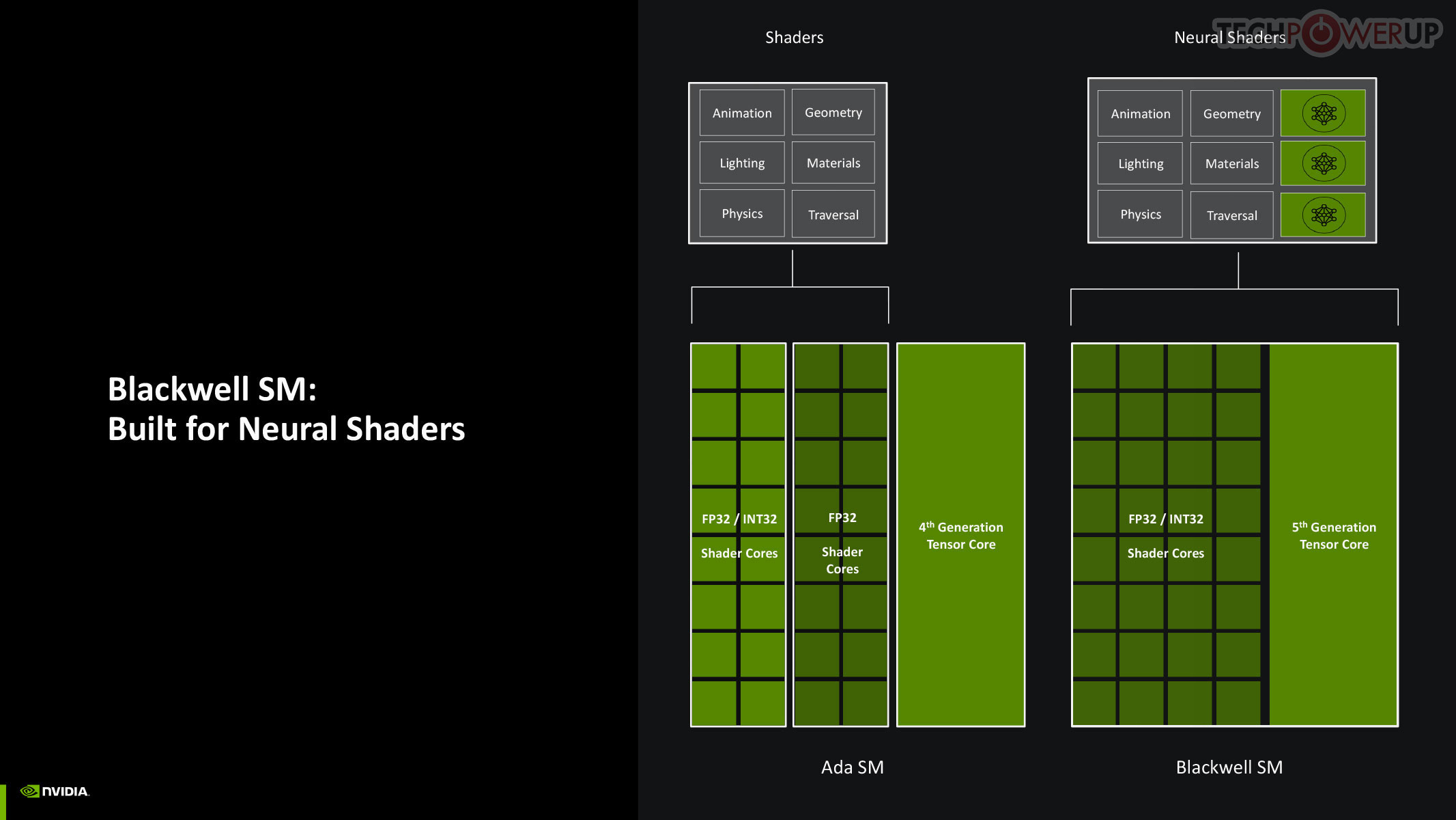
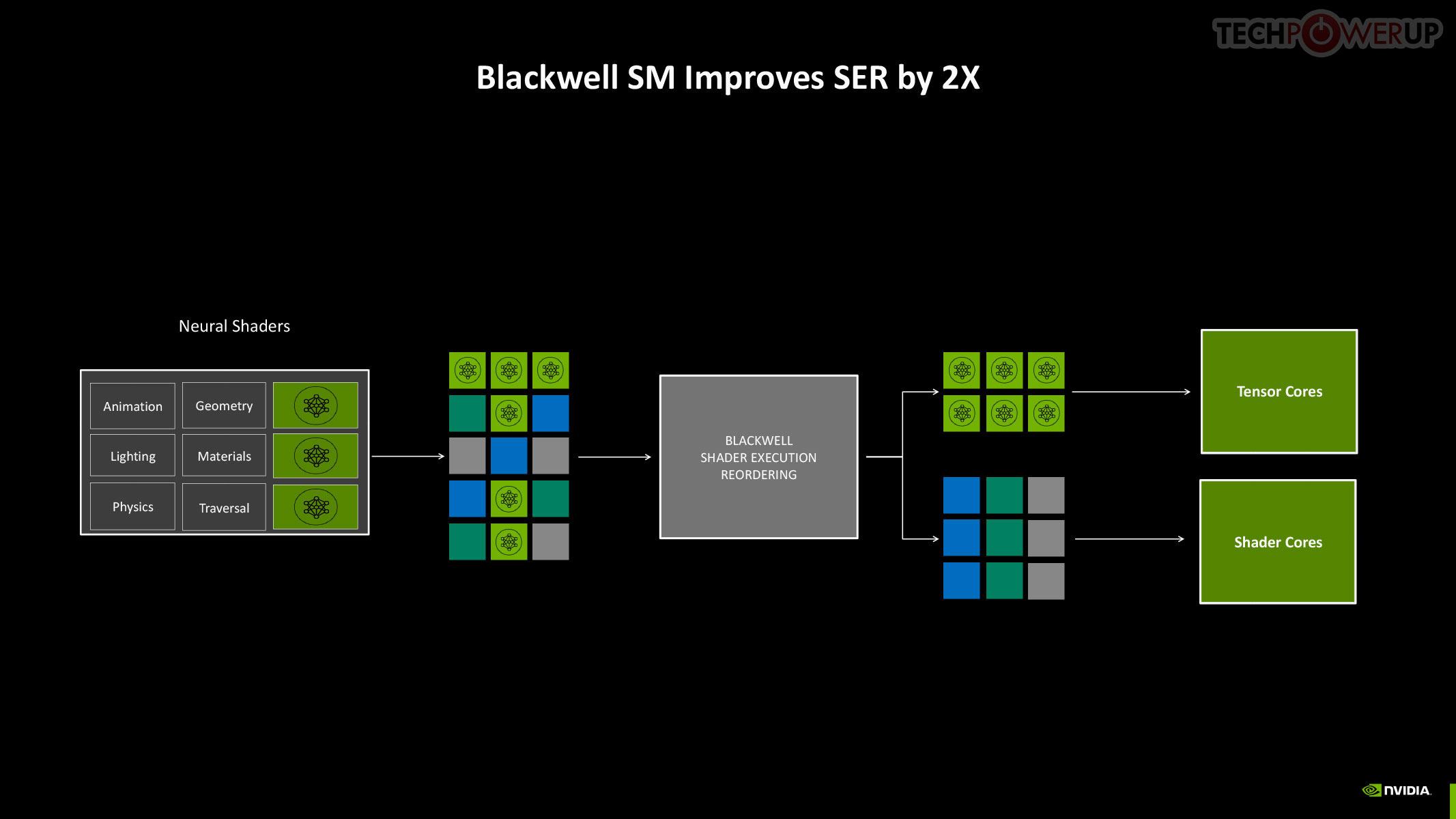
Perhaps the biggest change to the way the SM handles work, introduced with Blackwell, is the concept of neural shaders—treating portions of the graphics rendering workload done by a generative AI model as shaders. Microsoft has laid the groundwork for standardization of neural shaders with its Cooperative Vectors API, in the latest update to DirectX 12. The Tensor cores are now accessible for workloads through neural shaders, and the shader execution reordering (SER) engine of the Blackwell SM is able to more accurately reorder workloads for the CUDA cores and the Tensor core in an SM.
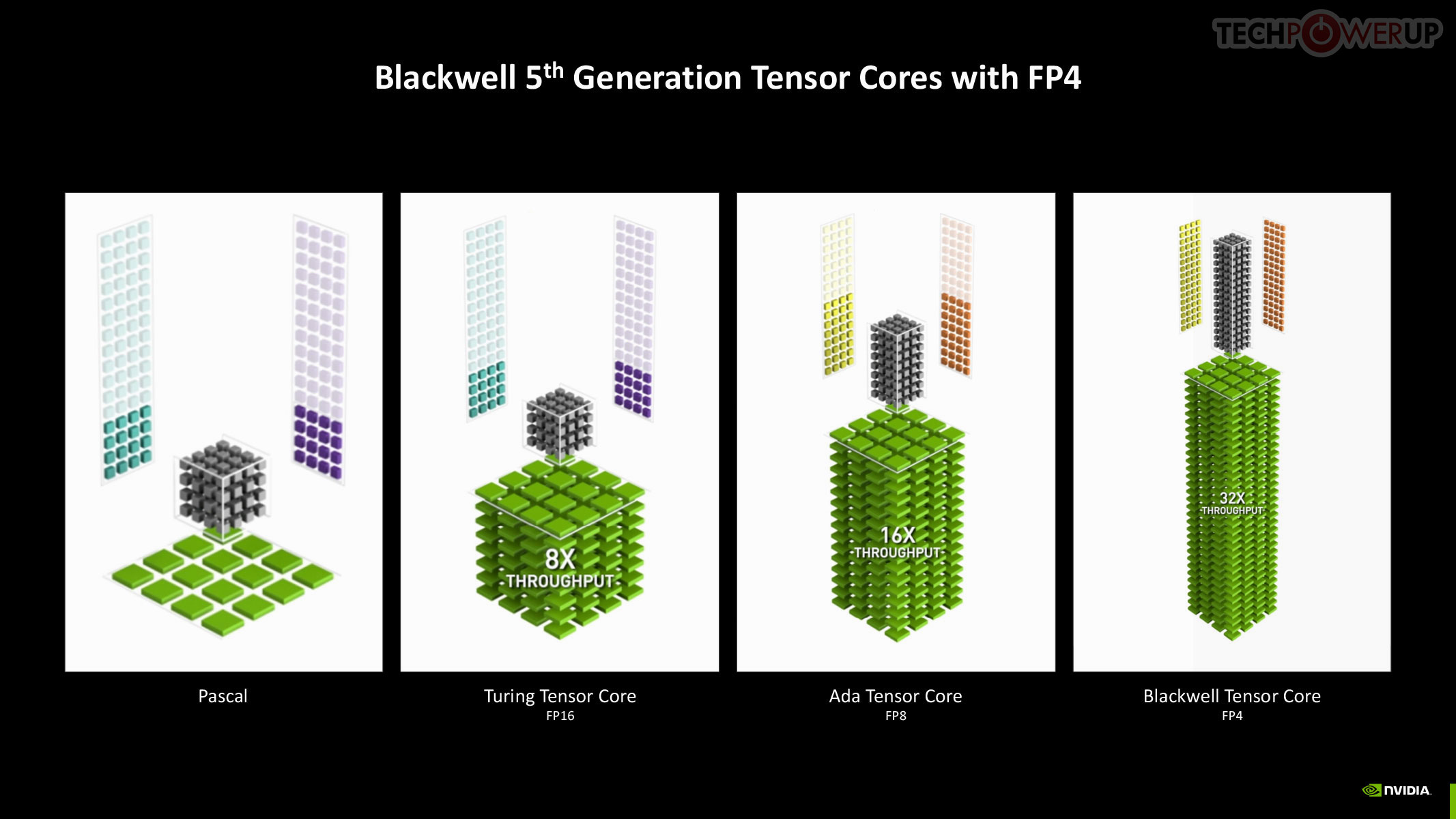
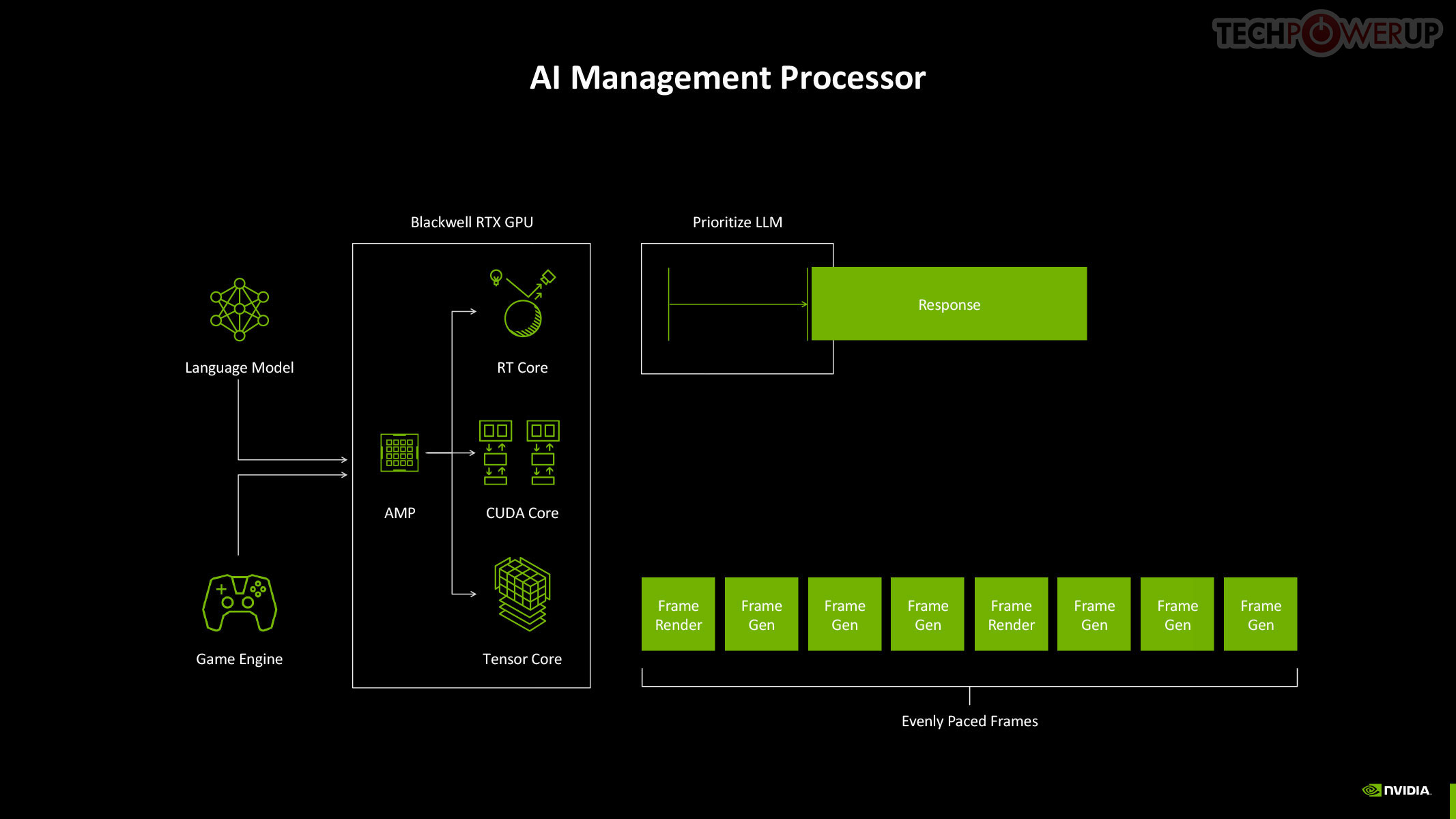
The new 5th Gen Tensor core introduces support for FP4 data format (1/8 precision) to fast moving atomic workloads, providing 32 times the throughput of the very first Tensor core introduced with the Volta architecture. Over the generations, AI models leveraged lesser precision data formats, and sparsity, to improve performance. The AI management processor (AMP) is what enables simultaneous AI and graphics workloads at the highest levels of the GPU, so it could be simultaneously rendering real time graphics for a game, while running an LLM, without either affecting the performance of the other. AMP is a specialized hardware scheduler for all the AI acceleration resources on the silicon. This plays a crucial role for DLSS 4 multi-frame generation to work.
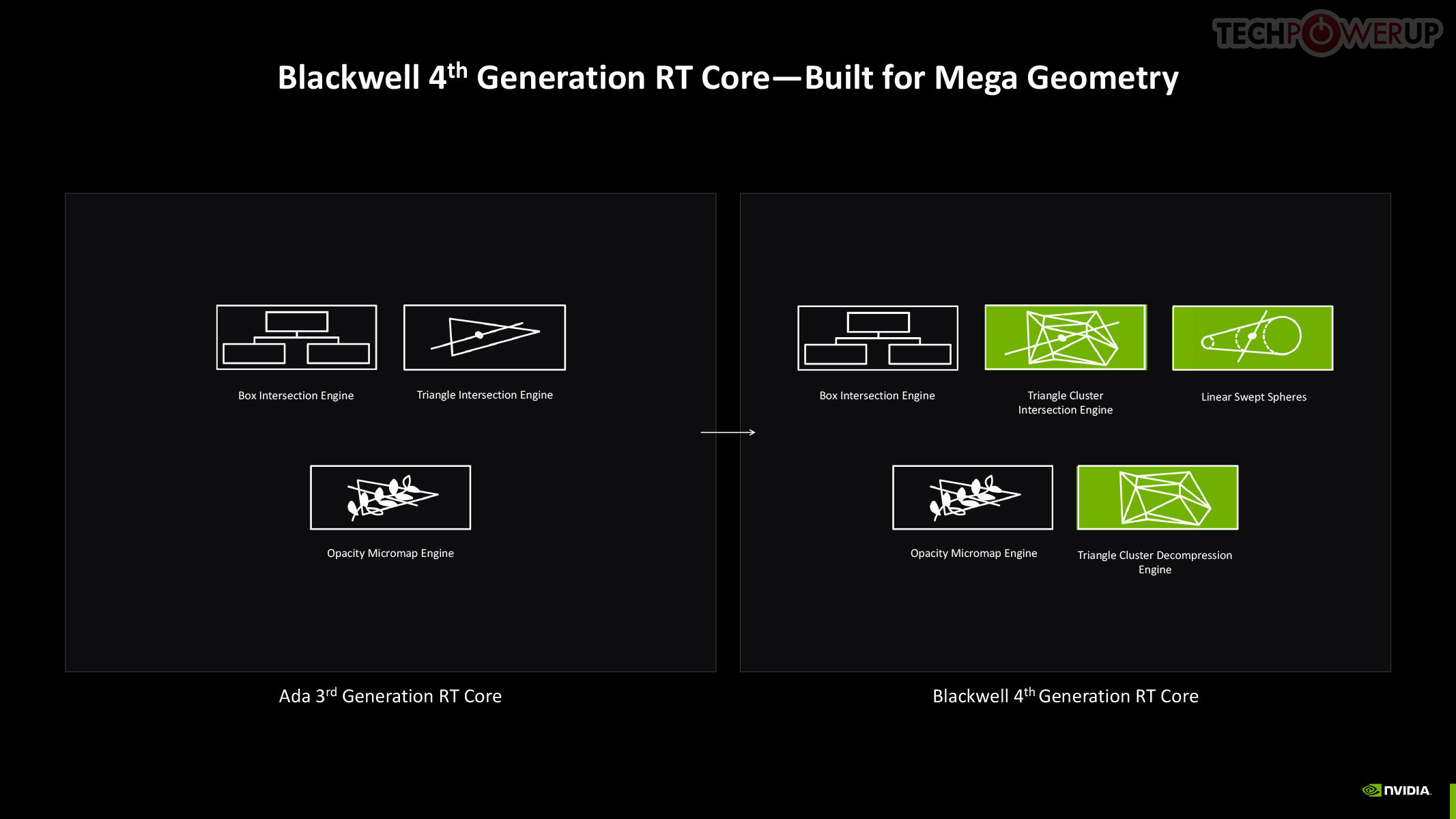
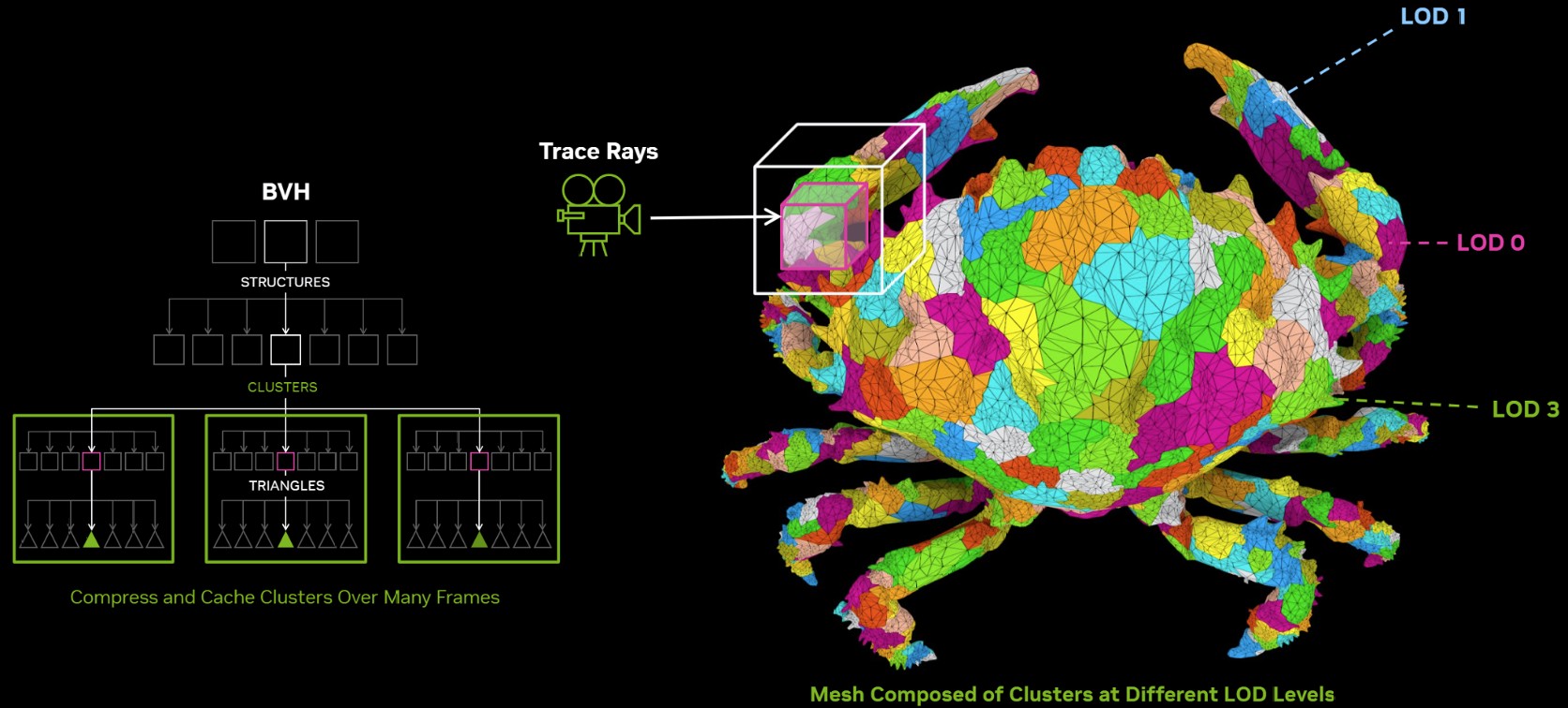
The 4th Gen RT core not just offers a generational increase in ray testing and ray intersection performance, which lowers the performance cost of enabling path tracing and ray traced effects; but also offers a potential generational leap in performance with the introduction of Mega Geometry. This allows for ray traced objects with extremely high polygon counts, increasing their detail. Poly count and ray tracing present linear increases in performance costs, as each triangle has to intersect with a ray, and there should be sufficient rays to intersect with each of them. This is achieved by adopting clusters of triangles in an object as first-class primitives, and cluster-level acceleration structures. The new RT cores introduce a component called a triangle cluster intersection engine, designed specifically for handling mega geometry. The integration of a triangle cluster compression format and a lossless decompression engine allows for more efficient processing of complex geometry.
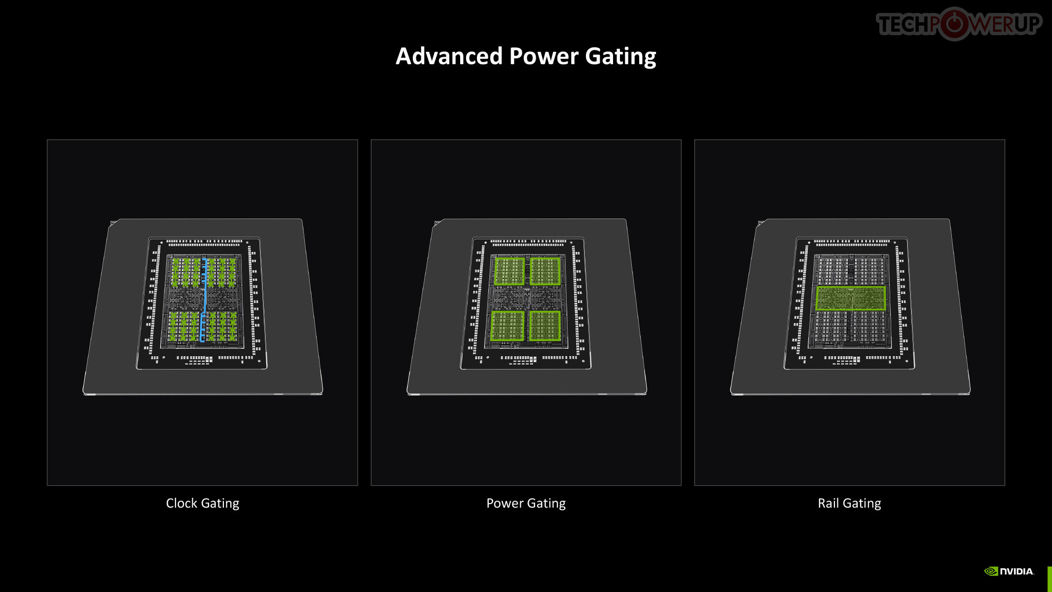
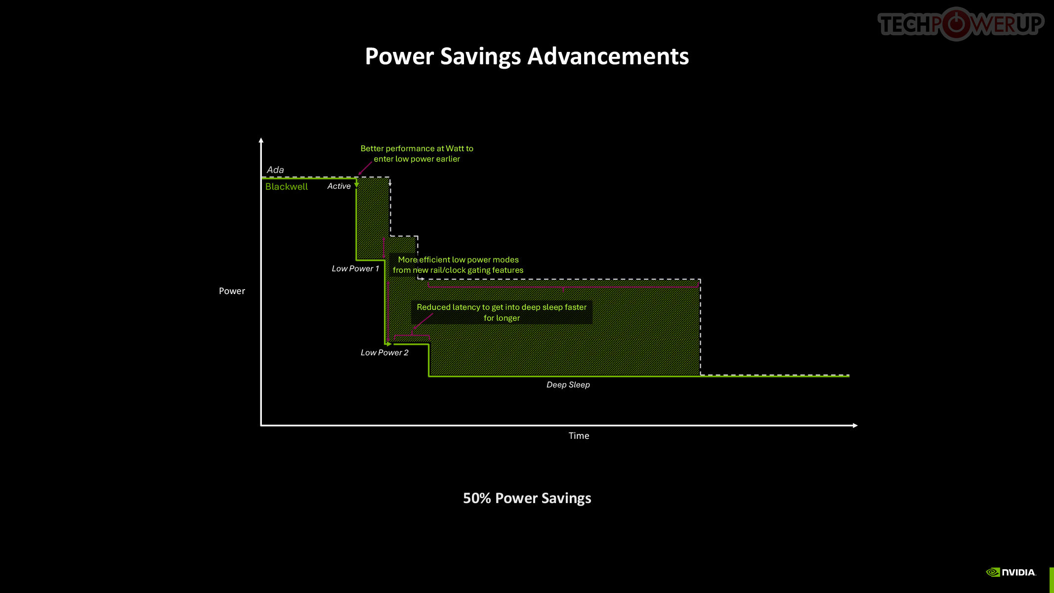
The GB206 and the rest of the GeForce Blackwell GPU family is built on the exact same TSMC "NVIDIA 4N" foundry node, which is actually 5 nm, as previous-generation Ada, so NVIDIA directed efforts to finding innovative new ways to manage power and thermals. This is done through a re-architected power management engine that relies on clock gating, power gating, and rail gating of the individual GPCs and other top-level components. It also worked on the speed at which the GPU makes power-related decisions.
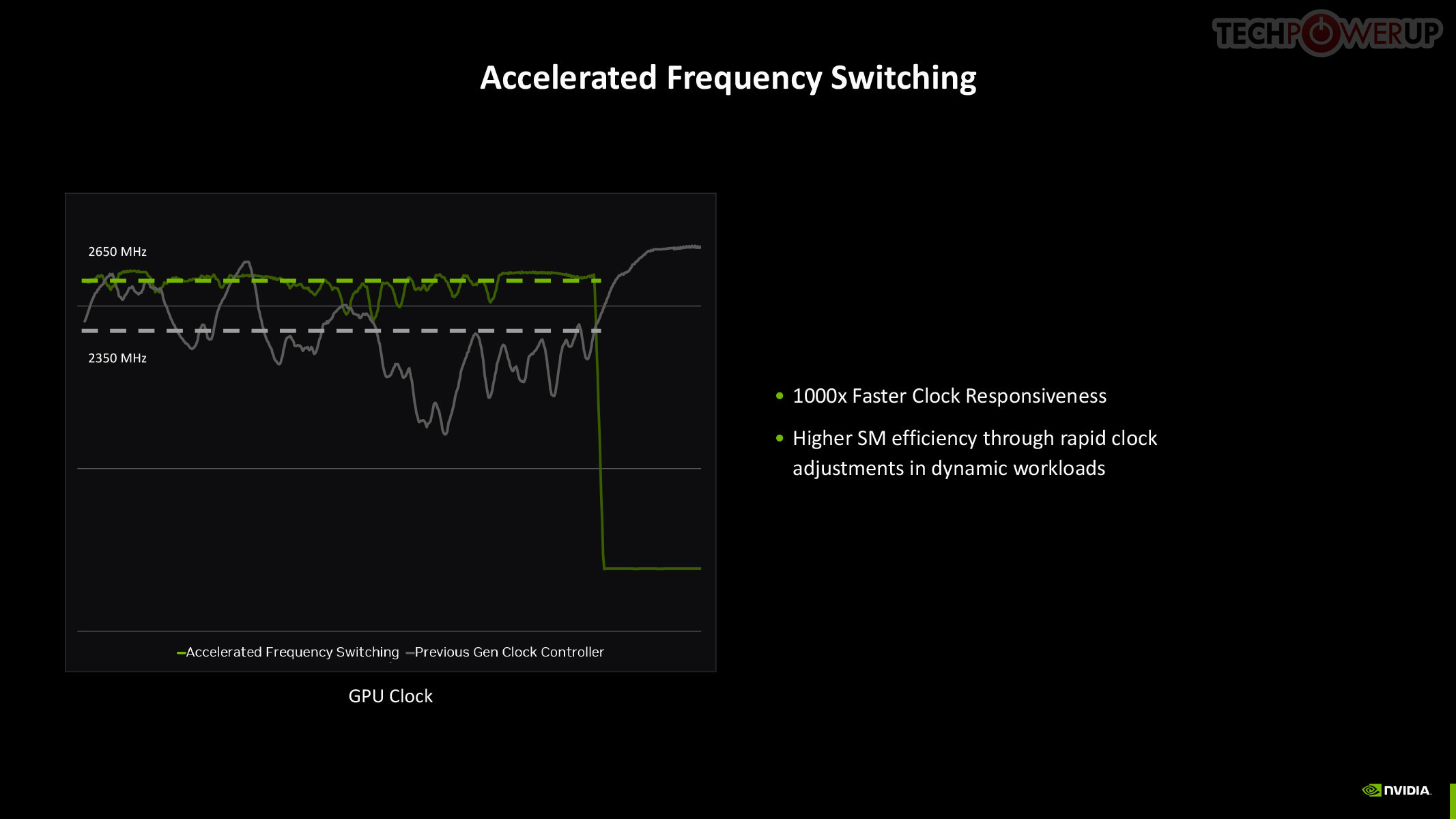
The quickest way to drop power is by adjusting the GPU clock speed, and with Blackwell, NVIDIA introduced a means for rapid clock adjustments at the SM-level.
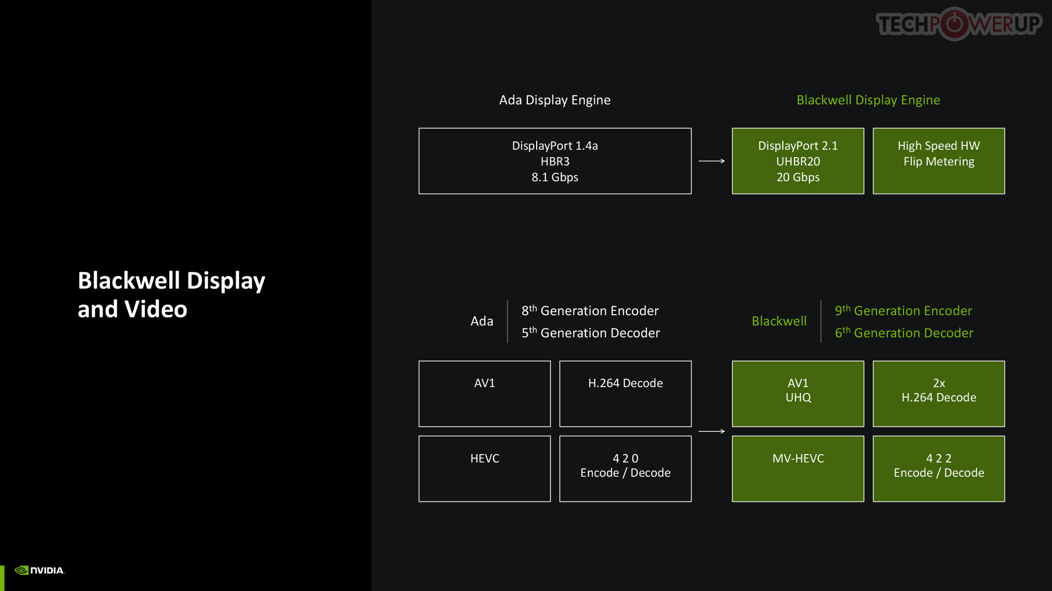
NVIDIA updated both the display engine and the media engine of Blackwell over the previous generation Ada, which drew some flack for holding on to older display I/O standards such as DisplayPort 1.4, while AMD and Intel had moved on to DisplayPort 2.1. The good news is that Blackwell supports DP 2.1 with UHBR20, enabling 8K 60 Hz with a single cable. The company also updated NVDEC and NVENC, which now support AV1 UHQ, double the H.264 decode performance, MV-HEVC, and 4:2:2 formats.
Neural Rendering
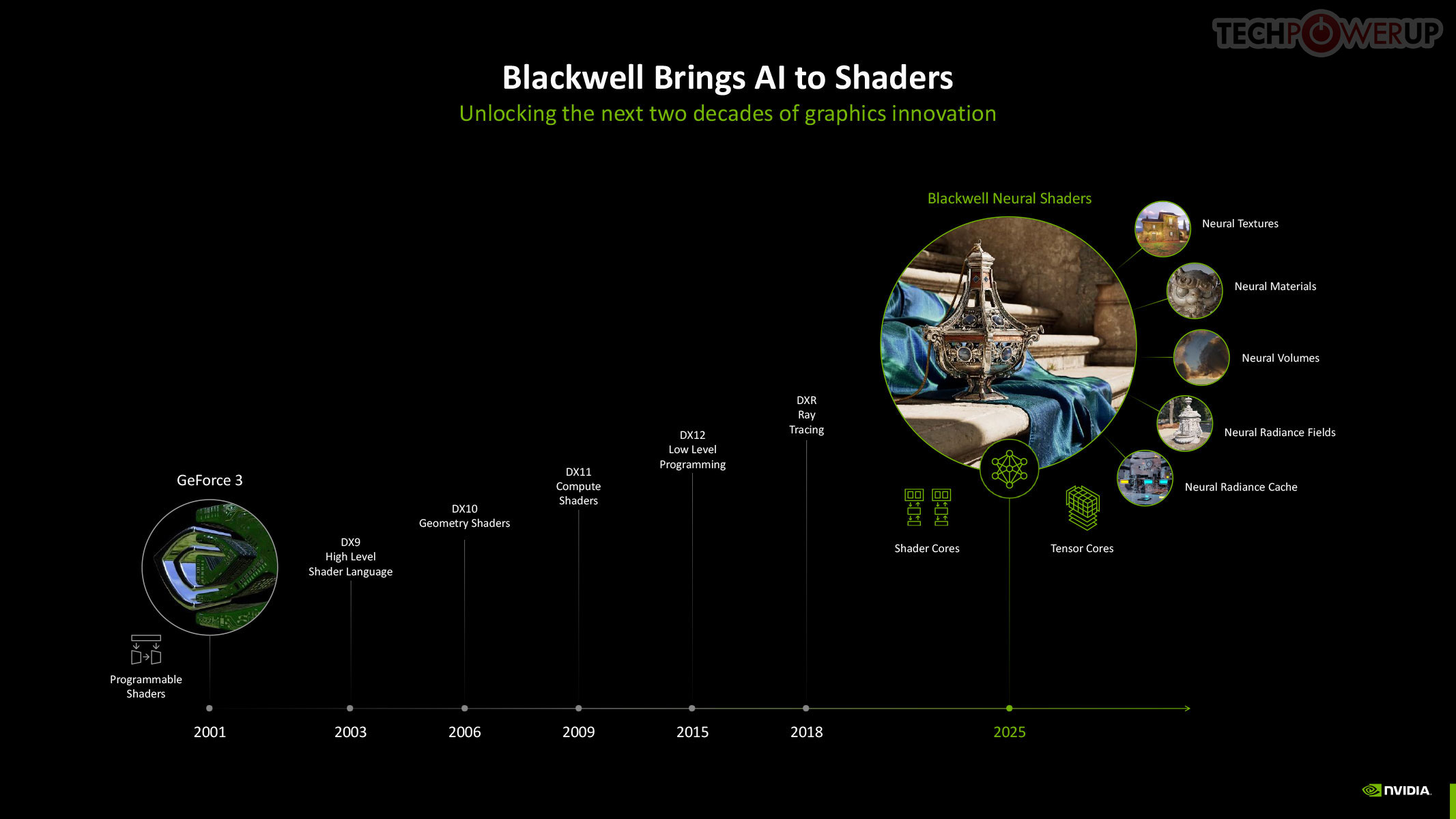
Neural Rendering promises to be as transformative to modern graphics as programmable shaders itself. 3D Graphics rendering evolved from fixed-function over the turn of the century, to programmable shaders, HLSL, geometry shaders, compute shaders, and ray tracing, over the past couple of decades. In 2025, NVIDIA is writing the next chapter in this journey with Blackwell neural shaders. This allows for a host of neural-driven effects, including neural materials, neural volumes, and even neural radiance fields. Microsoft introduced the new Cooperative Vectors API for DirectX in a recent update, making it possible to access Tensor cores within a graphics API. Combined with a new shading language, Slang, this breakthrough enables developers to integrate neural techniques directly into their workflows, potentially replacing parts of the traditional graphics pipeline. Slang splits large, complex functions into smaller pieces that are easier to handle. Given that this is a DirectX standard API feature, there is nothing that stops AMD and Intel from integrating Neural Rendering (Cooperative Vectors) into their graphics drivers.
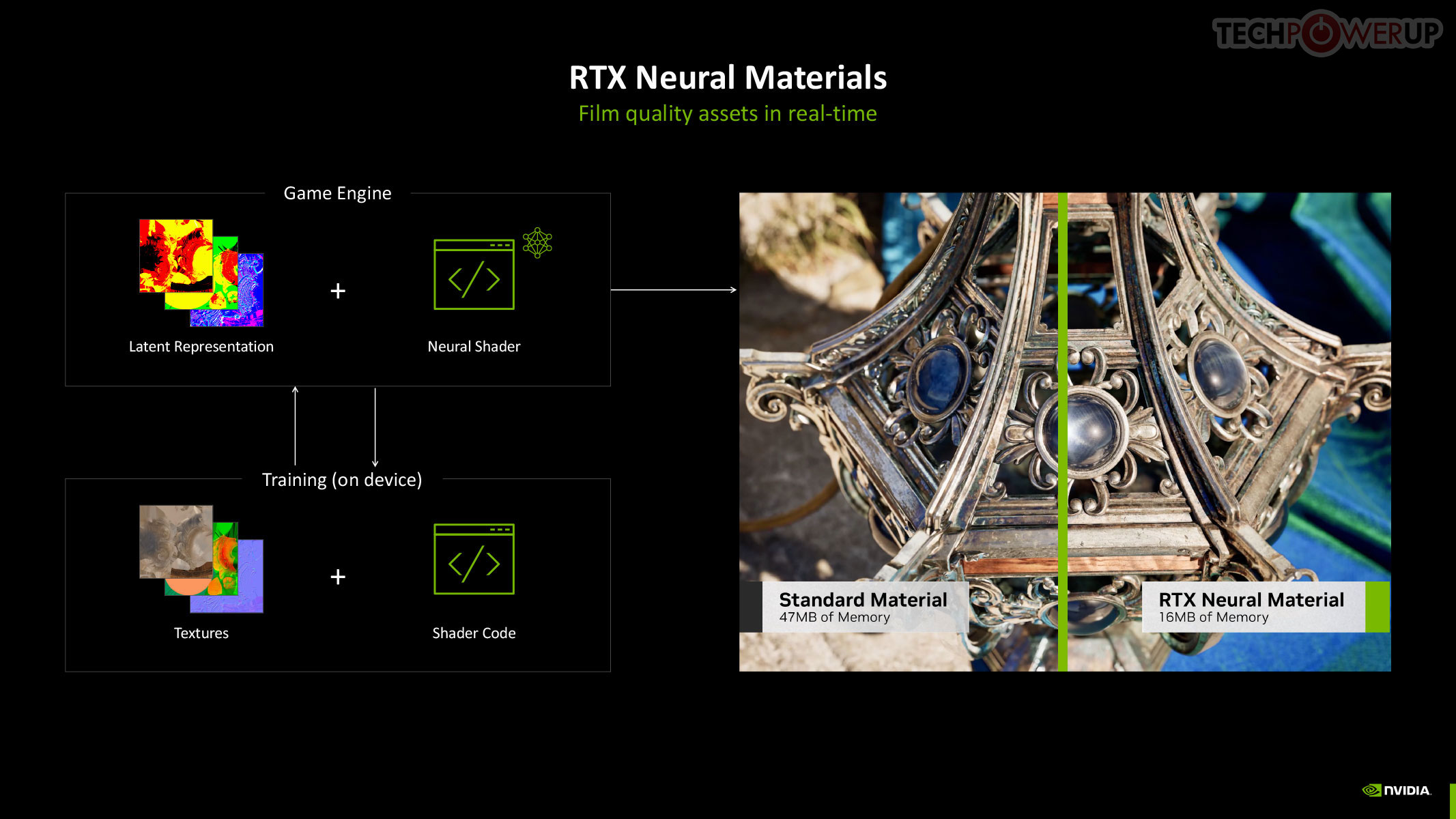
RTX Neural Materials works to significantly reduce the memory footprint of materials in 3D scenes. Under conventional rendering, the memory footprint of a material is bloated from complex shader code. Neural materials convert shader code and texture layers into a compressed neural representation. This results in up to a 7:1 compression ratio and enables small neural networks to generate stunning, film-like materials in real-time. For example, silk rendered with traditional shaders might lack the multicolored sheen seen in real life. Neural materials, however, capture intricate details like color variation and reflections, bringing such surfaces to life with unparalleled realism—and at a fraction of the memory cost.
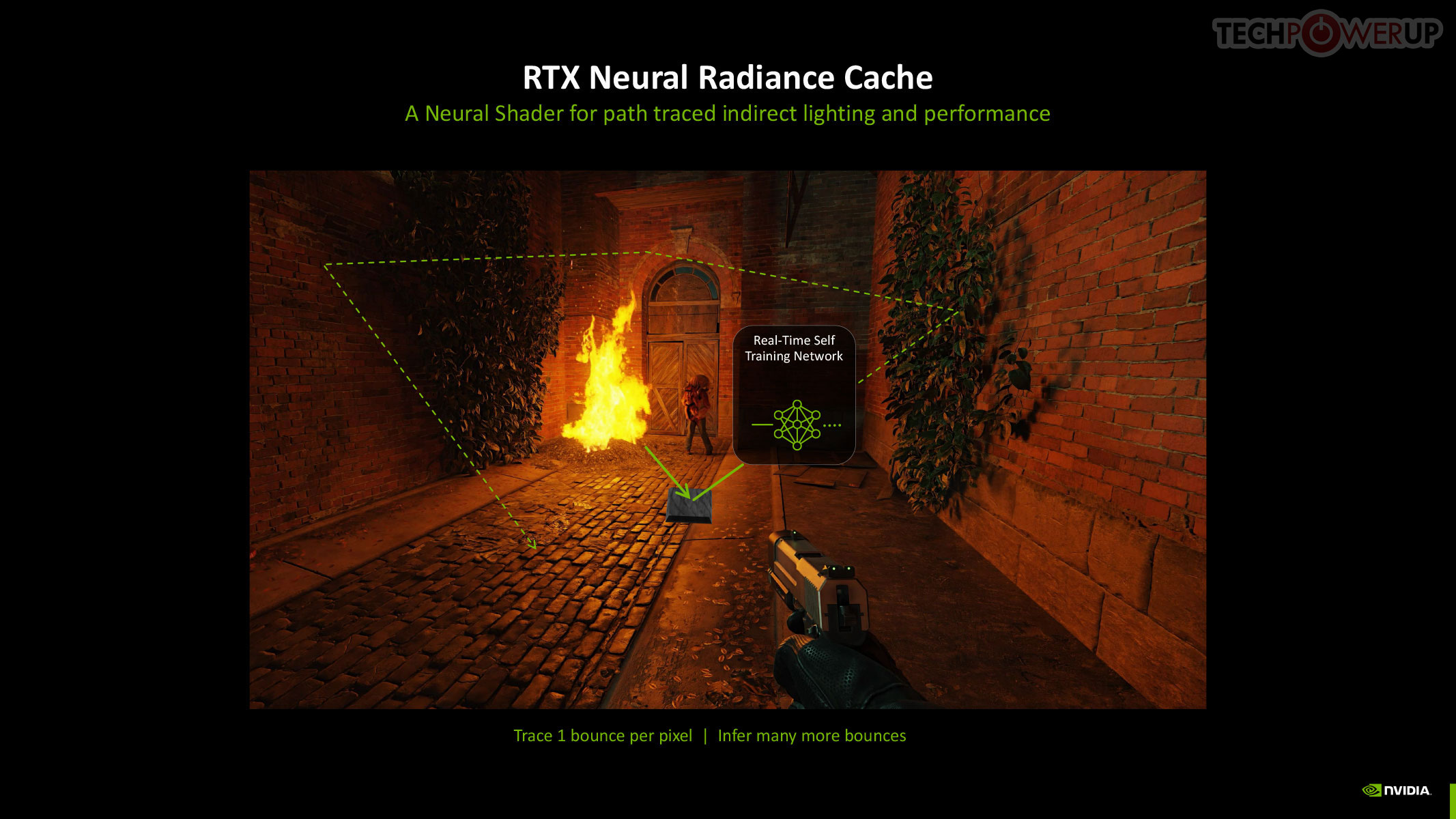
The new Neural Radiance Cache, which dynamically trains a neural network during gameplay using the user's GPU, allowing light transport to be cached spatially, enabling near-infinite light bounces in a scene. This results in realistic indirect lighting and shadows with minimal performance impact. NRC partially traces 1 or 2 rays before storing them in a radiance cache, and infers an infinite amount of rays and bounces for a more accurate representation of indirect lighting in the game scene.
DLSS 4 and Multi Frame Generation

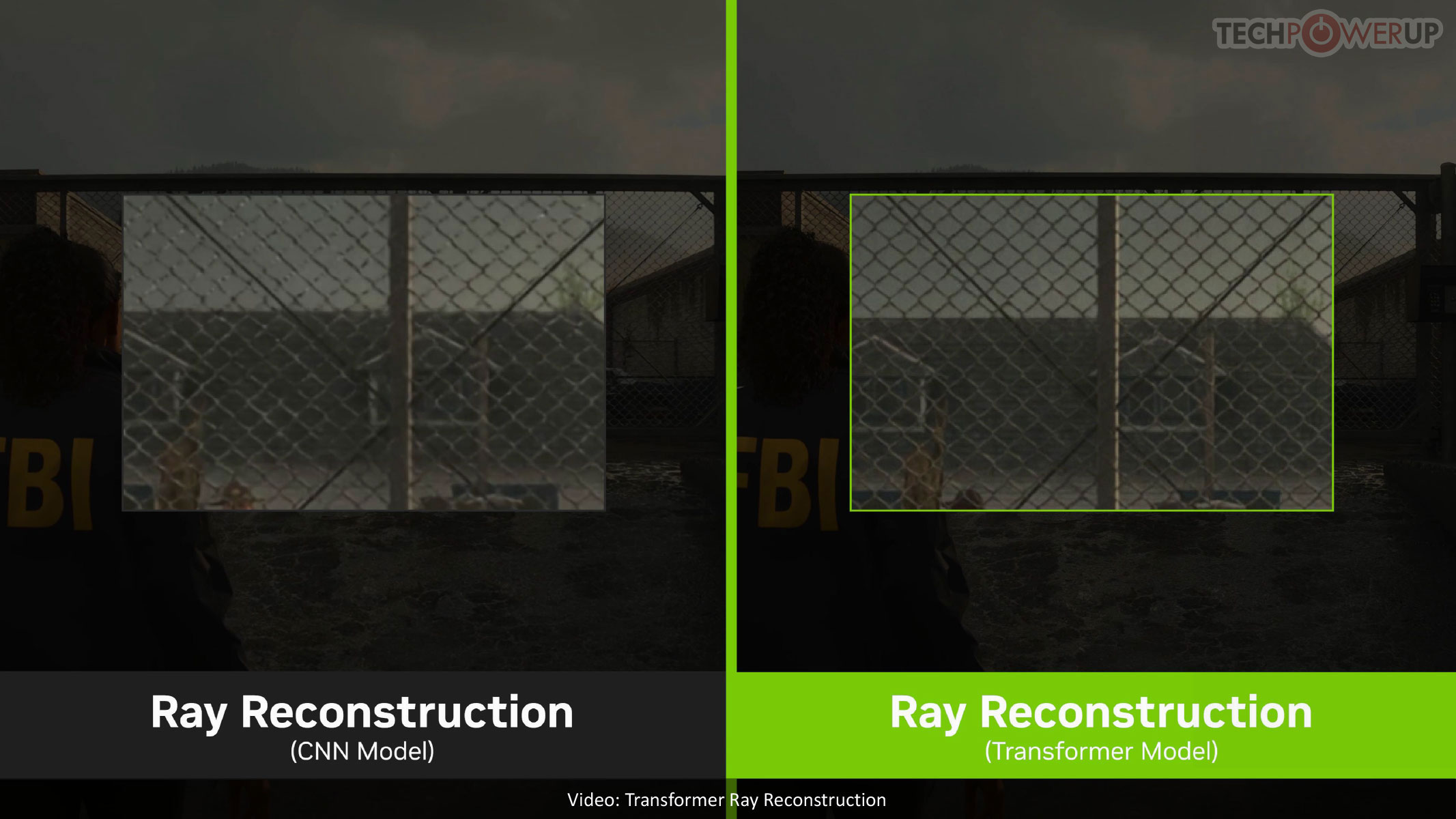
DLSS 4 introduces a major leap in image quality and performance. It isn't just a version bump with the introduction of a new feature, namely Multi Frame Generation, but introduces updates to nearly all DLSS sub-features. DLSS from its very beginning relied on AI to reconstruct details in super resolution, and with DLSS 4, NVIDIA is introducing a new transformer-based AI model to succeed the convolutional neural networks previous used, for double the parameters, four times the compute performance, and significantly improved image quality. Ray Reconstruction, introduced with DLSS 3.5, gets a significant image quality update with the new transformer-based model.
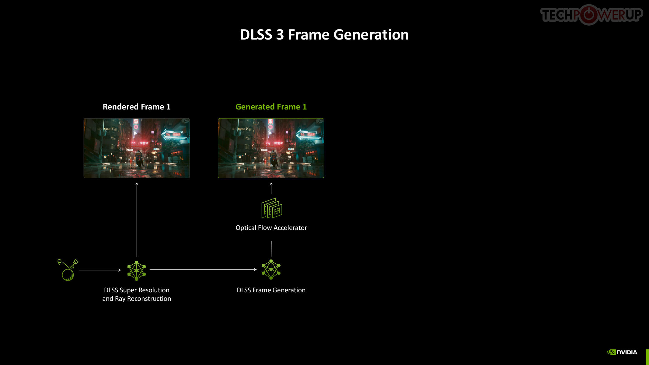
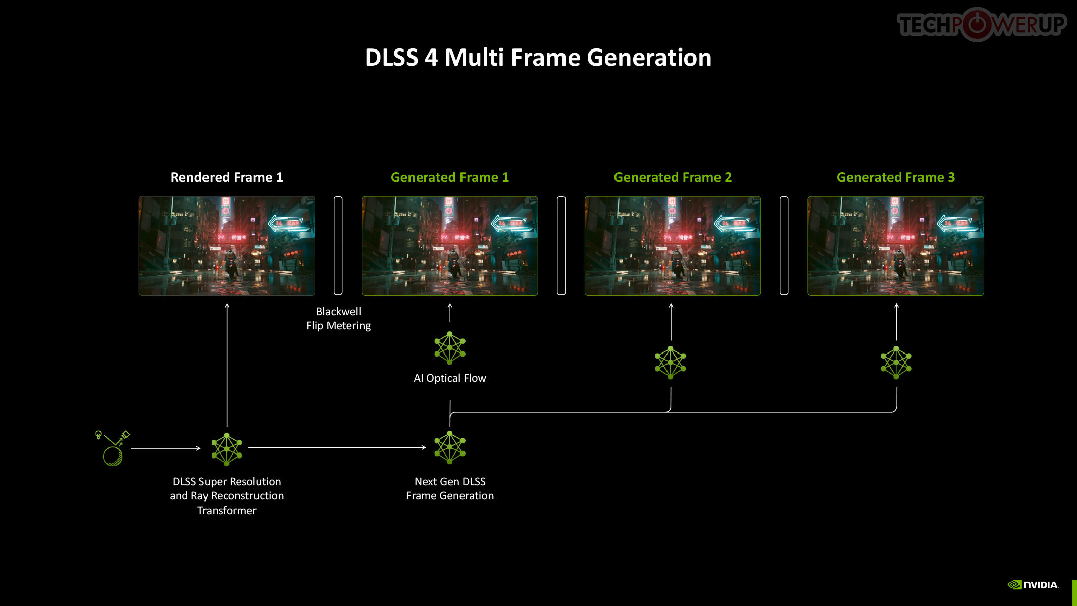
To understand Multi Frame Generation, you need to understand how DLSS Frame Generation, introduced with GeForce Ada, works. An Optical Flow Accelerator component gives the DLSS algorithm data to generate an entire frame using a neural network, using information from a previous rendered frame, effectively doubling frame rate. In Multi Frame Generation, AI takes over the functions of optical flow, to predict up to three frames following a conventionally rendered frame, effectively drawing four frames form the rendering effort of one.
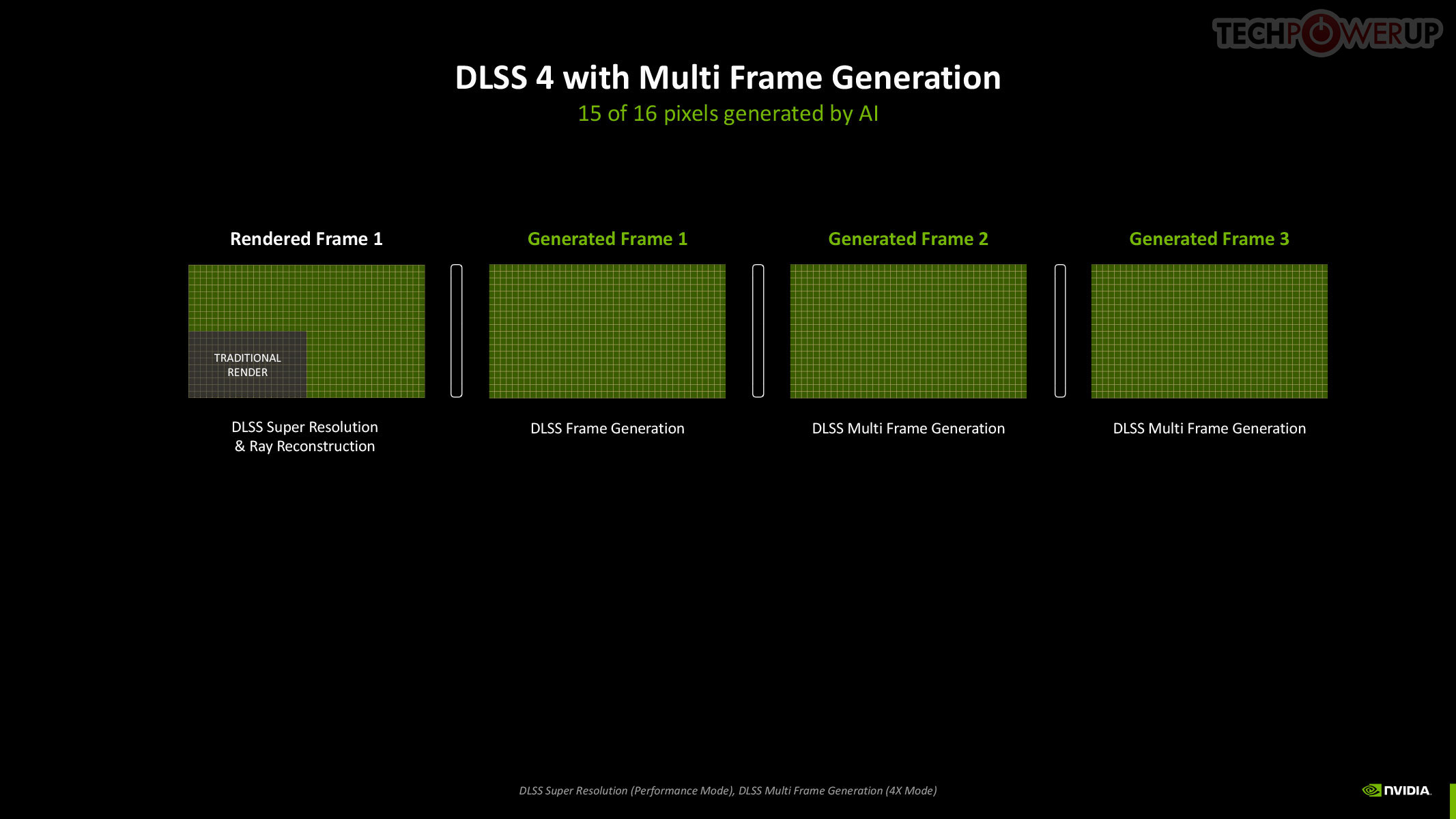
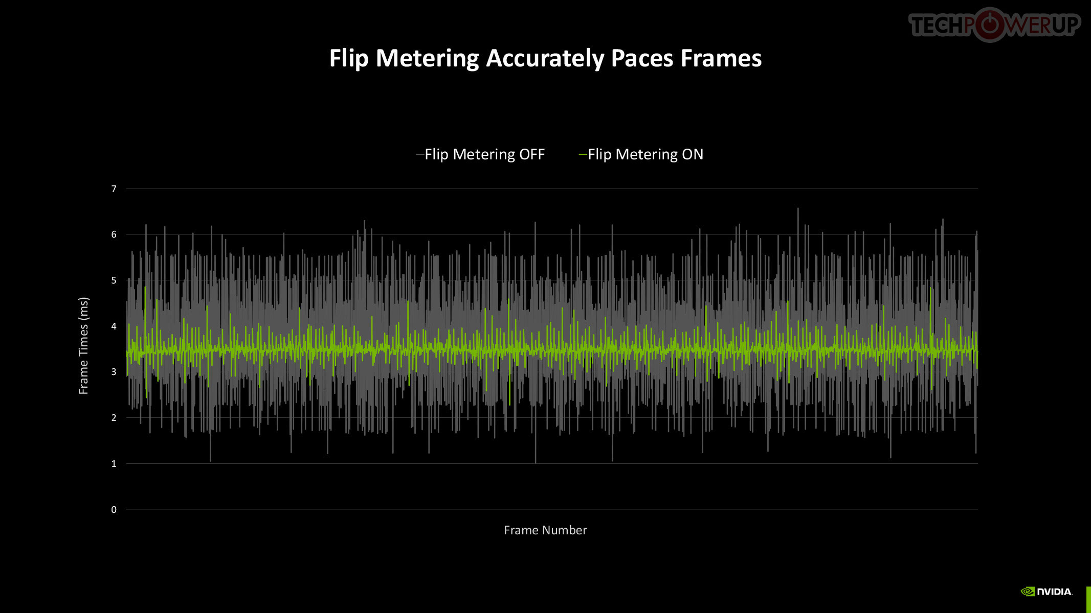
Now, assuming this rendered frame is a product of Super Resolution, with the maximum performance setting generating 4x the pixels from a single rendered pixel, you're looking at a possibility where the rendering effort of 1/4th a frame goes into drawing 4 frames, or 15 in every 16 pixels being generated entirely by DLSS. When generating so many frames, Frame Pacing becomes a problem—irregular frame intervals impact smoothness. DLSS 4 addresses these issues by using a dedicated hardware unit inside Blackwell, which takes care of flip metering, reducing frame display variability by 5-10x. The Display Engine of Blackwell contains the hardware for flip metering.
NVIDIA Reflex 2
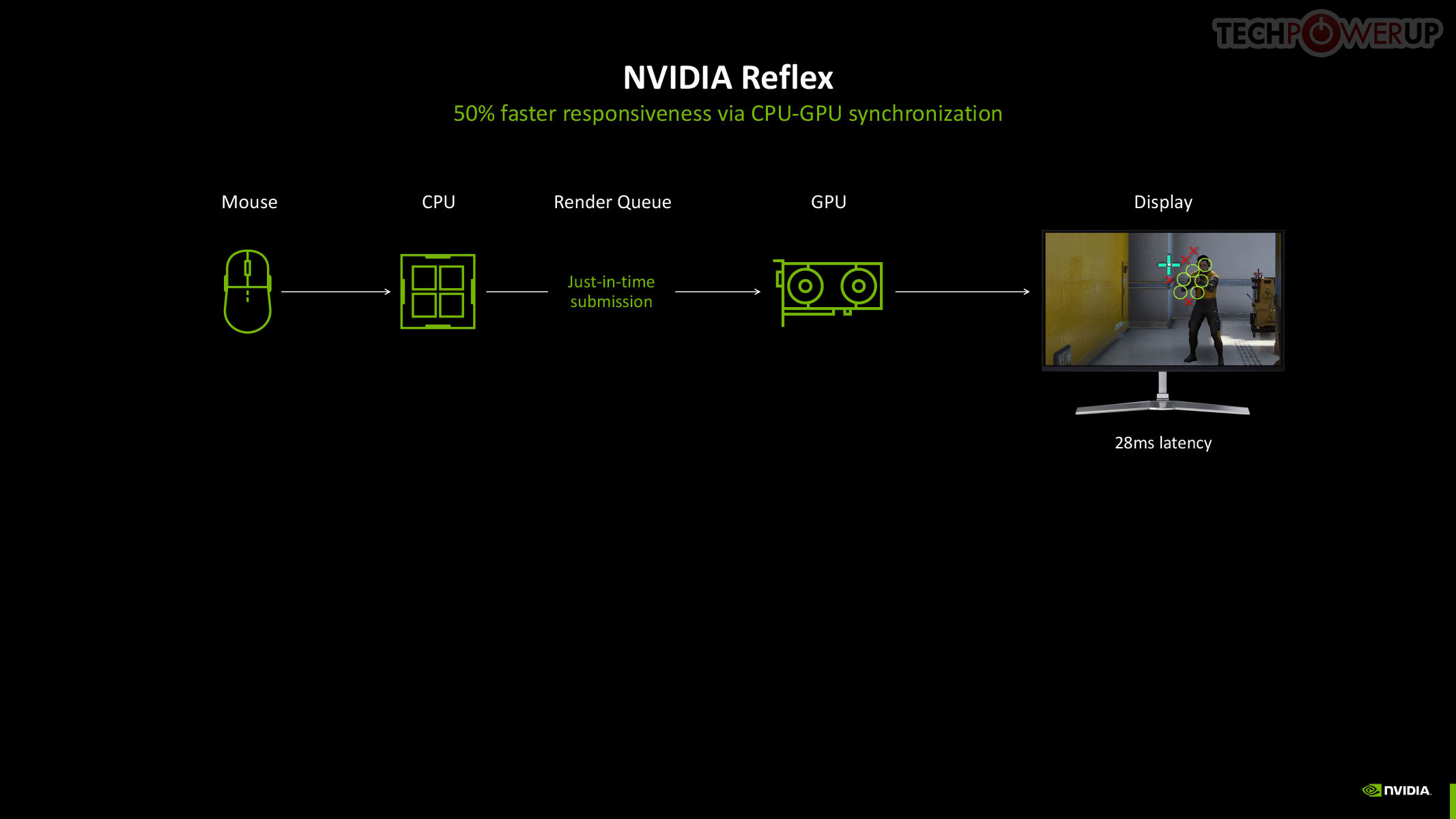
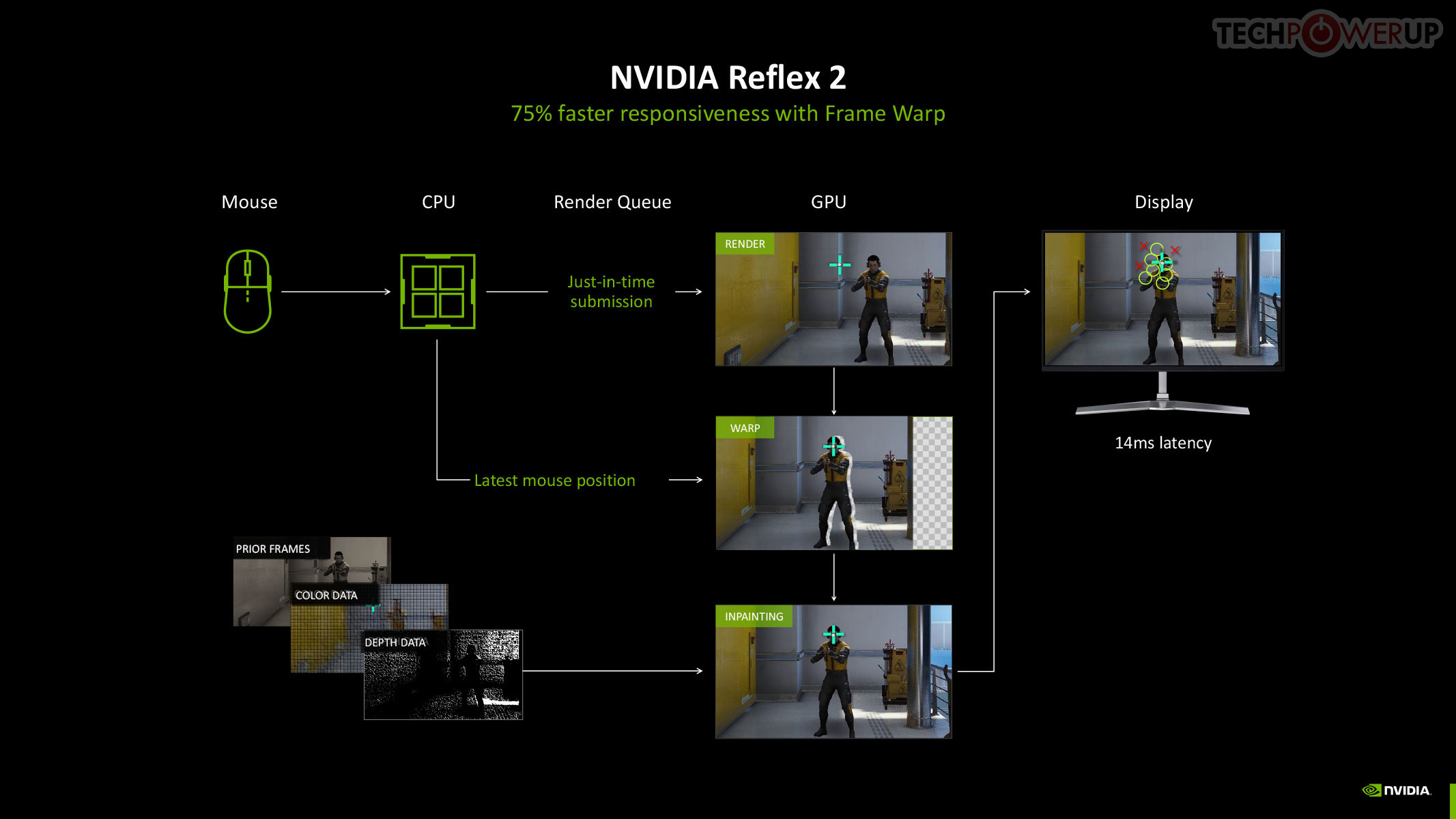
The original NVIDIA Reflex brought about a significant improvement to the responsiveness of maxed out graphics in competitive online gameplay, by compacting the rendering queue with the goal of reducing the whole system latency by up to 50%. Reflex is mandatory in DLSS 3 Frame Generation, given the latency cost imposed by the technology. Multi-frame generation calls for an equally savvy piece of technology, so we hence have Reflex 2. NVIDIA claims to have achieved a 75% reduction in latency with Frame Warp, which updates the camera (viewport) positions based on user inputs in real-time, and then uses temporal information to reconstruct the frame to display.
Packaging
The Card
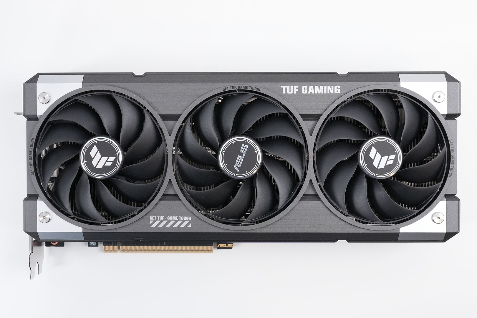
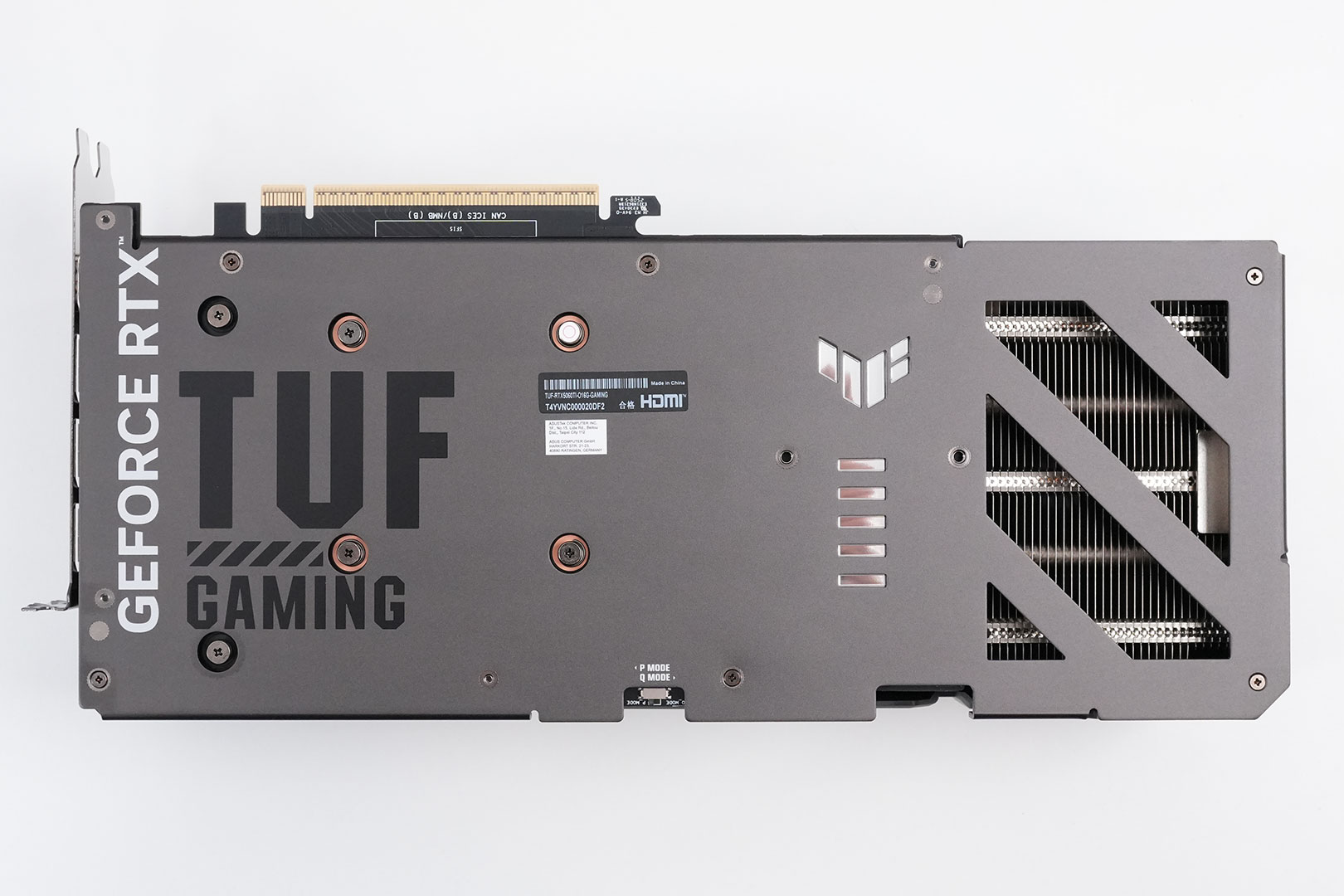
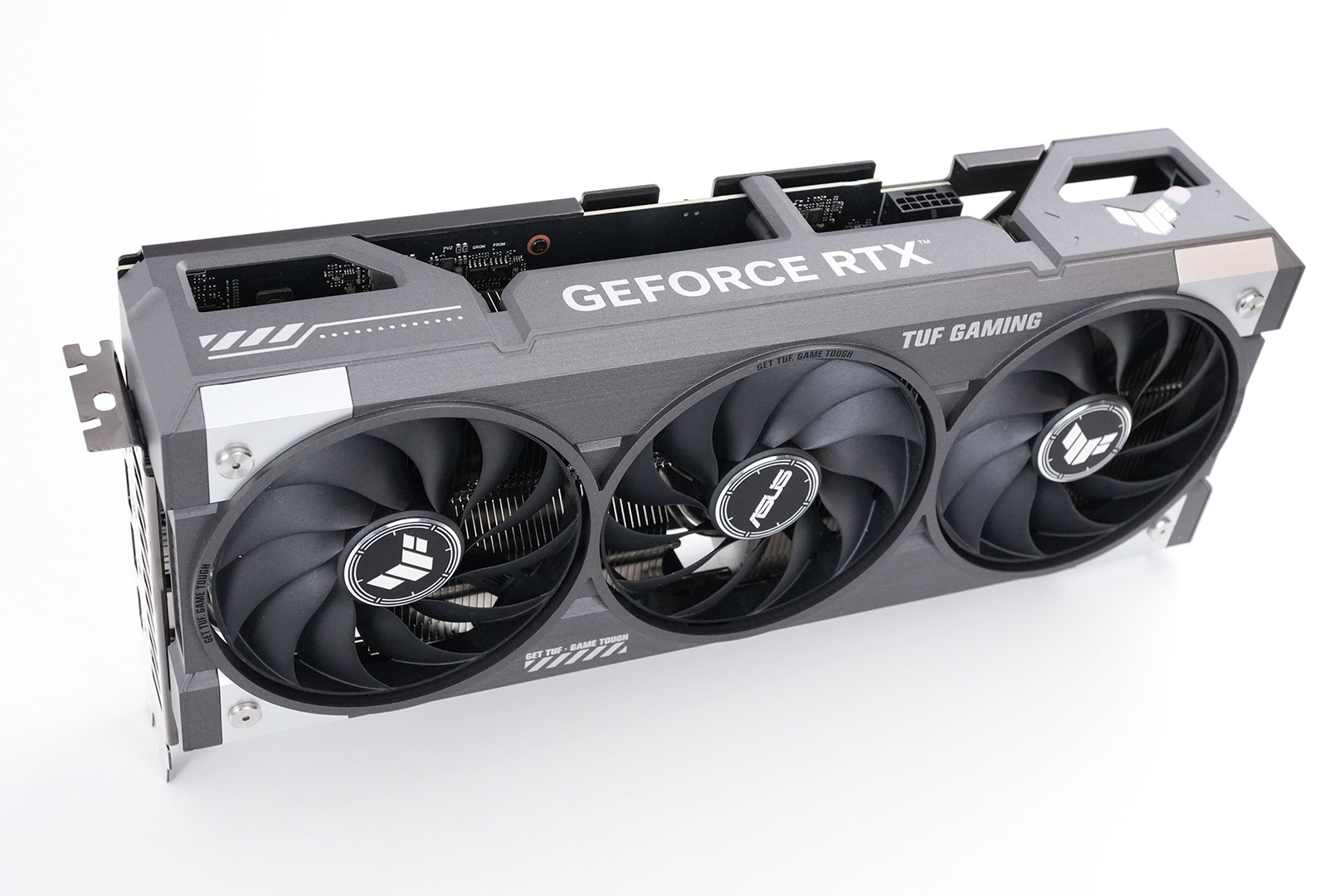
Visually, the ASUS RTX 5060 Ti TUF OC follows the design theme of the company's previous TUF cards, and it also matches the RX 9070 TUF visuals exactly. On the back you get a high quality metal backplate with a cutout for air to flow through.
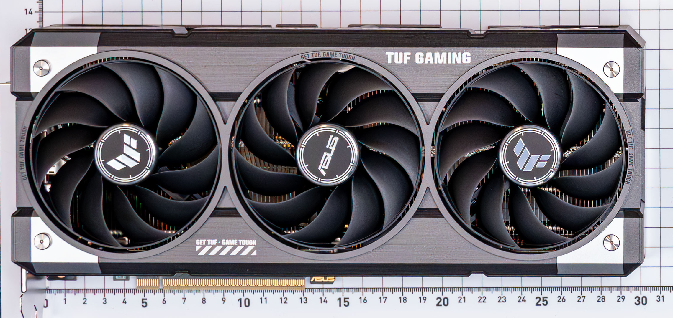
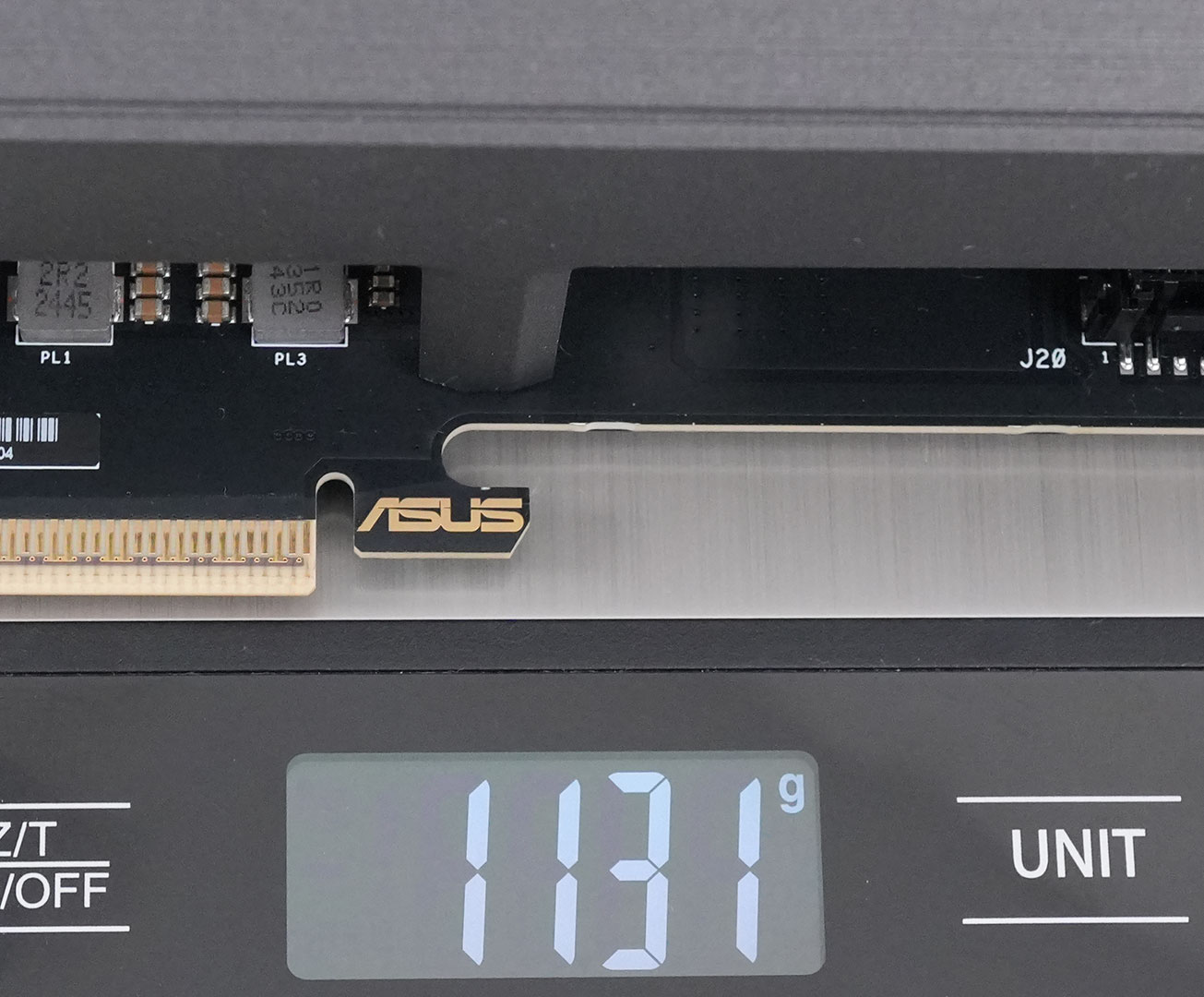
Dimensions of the card are 30.0 x 13.5 cm, and it weighs 1131 g.
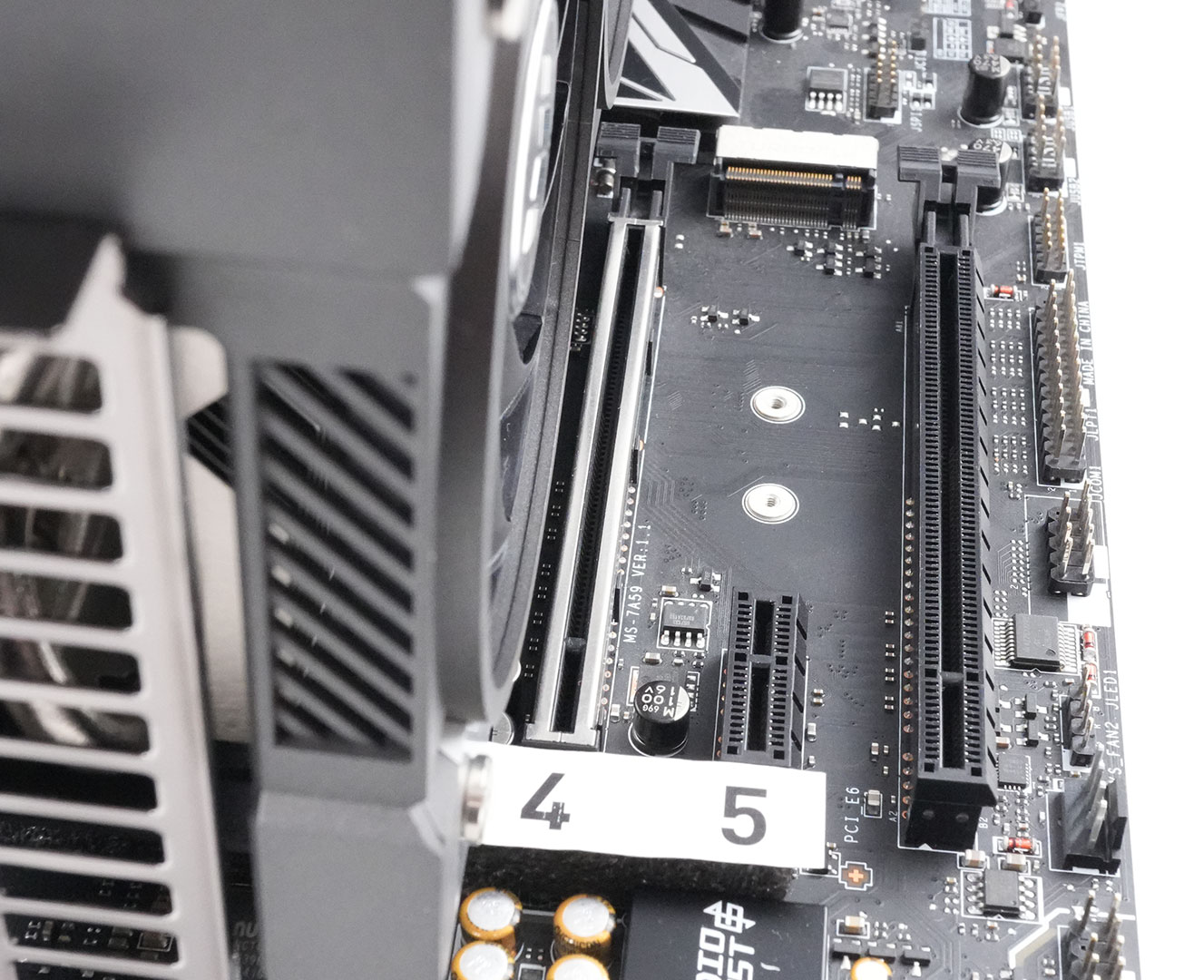

Installation requires three slots in your system. We measured the card's width to be 62 mm.
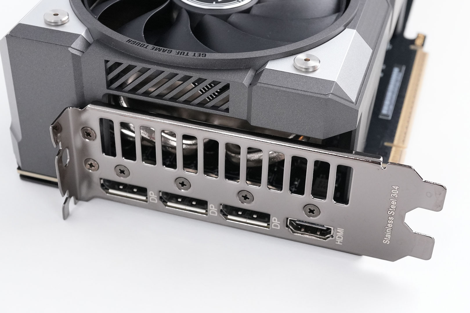
Display connectivity includes three standard DisplayPort 2.1b and one HDMI 2.1b.
Standard for all GeForce RTX 50-series Blackwell cards is a new display engine that supports three DisplayPort 2.1b outputs, each capable of UHBR20; and one HDMI 2.1a. Both interfaces support DSC (display stream compression). With DSC enabled, a single DisplayPort on this card can drive 4K 12-bit HDR at 480 Hz; or 8K 12-bit HDR at up to 165 Hz. The RTX 5060 Ti features an updated media acceleration engine with support for 4:2:2 video formats, AV1 UHQ, and MV-HEVC. Unlike the bigger RTX 50 models, which have two, there is a single NVENC and NVDEC unit each.
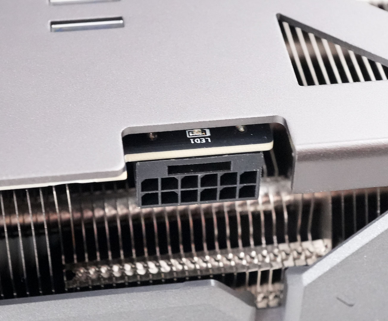
The card uses a single 16-pin connector, which, theoretically, allows a maximum power draw of 600 W. The card's power limit is set to 180 W, with up to 234 W allowed with manual increases.
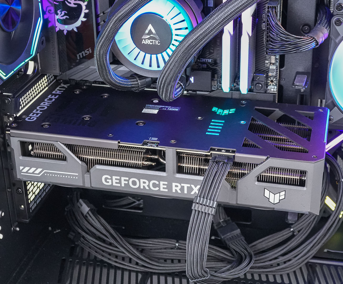
There's an RGB lighting zone on the backplate, near the TUF logo. The logo on the corner is not illuminated (unlike other TUF cards)
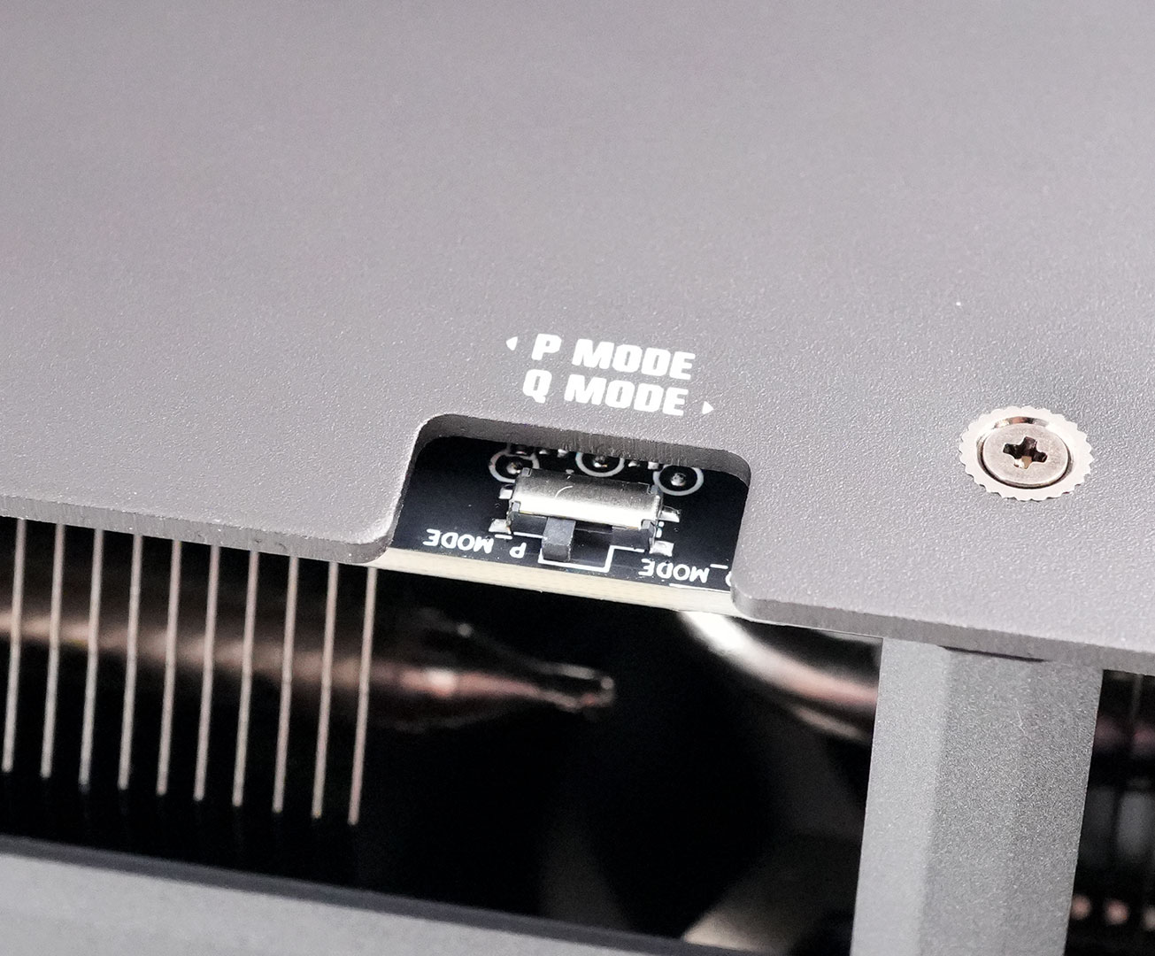
This BIOS switch lets you toggle between the default Performance BIOS and an optional "Quiet" BIOS.
Our Patreon Silver Supporters can read articles in single-page format.
Apr 24th, 2025 10:50 EDT
change timezone
Latest GPU Drivers
New Forum Posts
- To distill or not distill what say ye? (86)
- Are the 8 GB cards worth it? (141)
- The TPU UK Clubhouse (26168)
- I dont understand the phone OS world..... (20)
- Help me identify Chip of this DDR4 RAM (34)
- AAF Optimus Modded Driver For Windows 10 & Windows 11 - Only for Realtek HDAUDIO Chips (442)
- What are you playing? (23456)
- 5060 Ti 8GB DOA (263)
- New GPU 5070 Ti or better CPU Ryzen7 7800X3D ? (13)
- Microcenter GPU Stock status (85)
Popular Reviews
- NVIDIA GeForce RTX 5060 Ti 8 GB Review - So Many Compromises
- Colorful iGame B860M Ultra V20 Review
- ASUS GeForce RTX 5060 Ti TUF OC 16 GB Review
- ASRock X870E Taichi Lite Review
- Upcoming Hardware Launches 2025 (Updated Apr 2025)
- Sapphire Radeon RX 9070 XT Pulse Review
- Sapphire Radeon RX 9070 XT Nitro+ Review - Beating NVIDIA
- NVIDIA GeForce RTX 5060 Ti PCI-Express x8 Scaling
- AMD Ryzen 7 9800X3D Review - The Best Gaming Processor
- ASUS GeForce RTX 5080 TUF OC Review
Controversial News Posts
- NVIDIA GeForce RTX 5060 Ti 16 GB SKU Likely Launching at $499, According to Supply Chain Leak (182)
- NVIDIA Sends MSRP Numbers to Partners: GeForce RTX 5060 Ti 8 GB at $379, RTX 5060 Ti 16 GB at $429 (127)
- NVIDIA Launches GeForce RTX 5060 Series, Beginning with RTX 5060 Ti This Week (115)
- Nintendo Confirms That Switch 2 Joy-Cons Will Not Utilize Hall Effect Stick Technology (105)
- Nintendo Switch 2 Launches June 5 at $449.99 with New Hardware and Games (99)
- Sony Increases the PS5 Pricing in EMEA and ANZ by Around 25 Percent (85)
- NVIDIA PhysX and Flow Made Fully Open-Source (77)
- Windows Notepad Gets Microsoft Copilot Integration (75)