 126
126
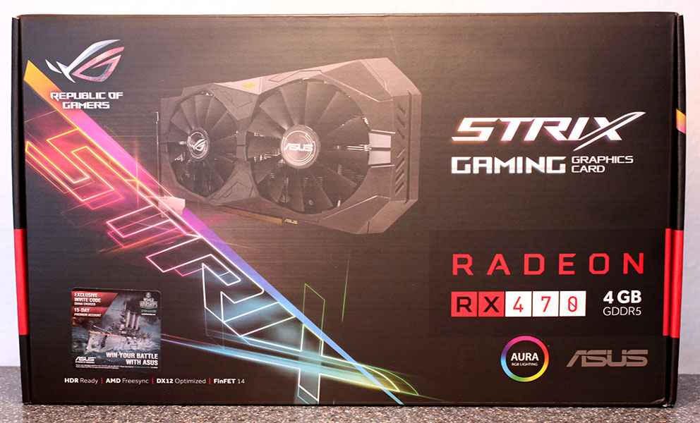
ASUS Radeon RX 470 STRIX OC 4 GB Review
(126 Comments) »Introduction
Even as NVIDIA has a somewhat top-down approach to the market with this generation by launching its top-performing "Pascal" GPUs in quick succession, including the "big chip" with the recent TITAN X Pascal, AMD's approach appears to be the opposite - bottom-up. The company debuted its "Polaris" architecture with GPUs that target the most voluminous market segment, $100-300, which AMD says to constitute the vast majority of discrete GPU sales.
Following up on the June launch of its $199-239 Radeon RX 480, AMD is launching the second, cheaper GPU based on the "Polaris" architecture, the Radeon RX 470. This SKU's price is expected to be below $200, although some custom-design cards, such as the ASUS Radeon RX 470 STRIX 4 GB we're reviewing today, could go slightly over it. This could confuse buyers because the 4 GB variant of the faster RX 480 is priced at $199 and gives you more performance.
The Radeon RX 470 is based on the same Polaris 10 "Ellesmere" silicon as the RX 480, featuring fewer shaders and lower clock speeds. The chip features 32 out of the 36 Graphics CoreNext (GCN) compute units (CUs) physically present on the chip, which makes for 2,048 stream processors. The TMU count is proportionately lowered to 128. The memory bus is untouched at 256-bit GDDR5, and the ROP count stays at 32. Reference clock speeds are set at 928 MHz core and 1206 MHz boost, and the memory runs at 6.6 Gbps, which works out to a bandwidth of 211 GB/s. ASUS overclocked its Radeon RX 470 STRIX graphics card to feature a boost frequency of 1270 MHz and left the memory untouched.

In this review, we have the ASUS Radeon RX 470 STRIX with us, which features the coveted Republic of Gamers STRIX branding and the company's all new DirectCU II cooling solution with an aluminum fin-stack heatsink that relies on two copper heat pipes that make direct contact with the GPU to draw heat away and to the fin stack. This heatsink is ventilated by a pair of 100 mm spinners, which don't spin at all when the GPU is idling. You also get an ROG emblem that glows in any of the 16.7 million colors across the RGB palette and a unique GPU-synced 4-pin PWM case-fan header feature ASUS is pioneering with this generation.
| GeForce GTX 960 | Radeon R9 380 | Radeon RX 470 | ASUS RX 470 STRIX OC | Radeon R9 380X | Radeon R9 390 | GeForce GTX 970 | Radeon RX 480 | Radeon R9 390X | GeForce GTX 980 | GeForce GTX 1060 | |
|---|---|---|---|---|---|---|---|---|---|---|---|
| Shader Units | 1024 | 1792 | 2048 | 2048 | 2048 | 2560 | 1664 | 2304 | 2816 | 2048 | 1280 |
| ROPs | 32 | 32 | 32 | 32 | 32 | 64 | 56 | 32 | 64 | 64 | 48 |
| Graphics Processor | GM206 | Tonga | Ellesmere | Ellesmere | Tonga | Hawaii | GM204 | Ellesmere | Hawaii | GM204 | GP106 |
| Transistors | 2940M | unknown | 5700M | 5700M | unknown | 6200M | 5200M | 5700M | 6200M | 5200M | 4400M |
| Memory Size | 2 GB | 2 GB | 4 GB | 4 GB | 4 GB | 8 GB | 4 GB | 4 GB / 8 GB | 8 GB | 4 GB | 6 GB |
| Memory Bus Width | 128 bit | 256 bit | 256 bit | 256 bit | 256 bit | 512 bit | 256 bit | 256 bit | 512 bit | 256 bit | 192 bit |
| Core Clock | 1127 MHz+ | 970 MHz | 1206 MHz | 1270 MHz | 970 MHz | 1000 MHz | 1051 MHz+ | 1266 MHz | 1050 MHz | 1126 MHz+ | 1506 MHz+ |
| Memory Clock | 1753 MHz | 1375 MHz | 1650 MHz | 1650 MHz | 1425 MHz | 1500 MHz | 1750 MHz | 2000 MHz | 1500 MHz | 1750 MHz | 2002 MHz |
| Price | $170 | $165 | $180 | $210 | $210 | $260 | $265 | $200 / $240 | $310 | $360 | $250 / $300 |
Architecture
At the heart of the Radeon RX 470 is the new "Ellesmere" (Polaris 10) GPU built on the 14 nanometer silicon fab process by Samsung and GlobalFoundries. The wafers are made in Upstate New York, USA, and are then bumped and packaged at a facility in Taiwan to be sent to the various graphics card manufacturers located there and across the straits.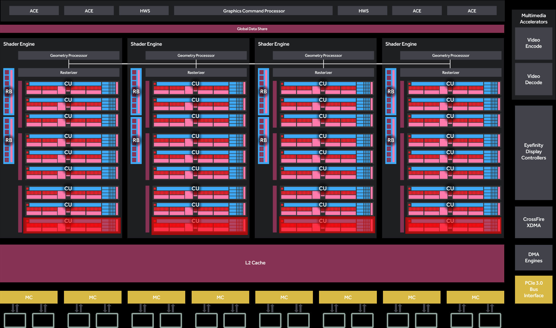

This GPU is based on AMD's fourth generation Graphics CoreNext architecture codenamed "Polaris." According to AMD, Compute Units (CUs) based on Polaris are 15% more efficient at number crunching than CUs based on the preceding Graphics CoreNext 1.2 architecture (R9 Fury, R9 380X). Pay attention to the numbers here. While the number-crunching machinery is 15% more efficient, the chip is claimed to have a 2.5x leap in overall energy-efficiency over the previous generation. This is because AMD is cashing in on the immediate gains a new silicon fab process brings to the table, the 14 nm FinFET process in this case, to increase transistor counts and clock speeds.

The component hierarchy in the Polaris 10 "Ellesmere" silicon is similar to older-generation chips, although each of the components received major updates. We begin with the chip featuring two hardware schedulers and the introduction of dedicated real-time asynchronous compute with spatial and temporal scheduling. The chip also features four async compute engines (ACEs). AMD optimized the async compute engine with new quick-response queue tech.


There's a design focus on stepping up geometry processing performance and blunting the brute-tessellation advantage NVIDIA traditionally enjoyed over AMD. For a chip of this segment, Polaris 10 features four independent geometry processors. Their functionality is upgraded over the previous generation, featuring a primitive discard accelerator which culls (discards) triangles in the pipeline with zero area or no inclusive sample points. The geometry engine now features a tiny cache called the Index Cache, which cushions small instanced geometry and reduces data movement to improve primitive throughput during instancing.
The Polaris 10 silicon features 36 Compute Units (CUs). 32 of these are enabled on the RX 470, spread across four shader engines, each with a dedicated geometry processor, a raster engine, and two render backends. The four shader engines are supported by a large 2 MB L2 cache, which acts as the town-square for the GPU's various key components.
Most of the architecture-specific innovations are centered on the CU, which now features a hardware instruction prefetcher, a larger instruction buffer, and native half-precision (FP16/Int16) support, which should reliably crunch numbers for gaming applications with significantly reduced memory and register footprints while lowering power execution. Altogether, the "Polaris" CU is claimed to have up to 15% higher performance than CUs based on the GCN 1.1 architecture (R9 390X). Each CU features 64 stream processors, which has the 32 CUs amount to 2,048 stream processors. In summary, the Polaris 10 chip features 2,048 stream processors, 128 TMUs, and 32 ROPs.


The Radeon RX 470 features a 256-bit wide GDDR5 memory interface, holding 4 GB or 8 GB of memory, clocked at 6.6 Gbps. The actual memory bandwidth of this interface at its given clock speeds is rated at up to 211 GB/s, although its effective bandwidth could be higher thanks to an updated lossless delta color compression (DCC) tech with full 2/4/8:1 compression ratios. AMD claims that its new gen DCC tech can provide an effective bandwidth uplift of a staggering 30 percent. The ASUS Radeon RX 470 STRIX we're reviewing today features 4 GB of memory.


The multimedia accelerators receive a major update, now supporting H.265 Main10 decode hardware acceleration and 4K60 HEVC encode hardware acceleration. The other components with big updates are the display controllers, which now support DisplayPort 1.4 (DP 1.3 HBR3 and DP 1.4 HDR) and HDMI 2.0b. FreeSync is supported over both DP and HDMI. Resolutions as high as 5K60, 10-bit 4K96 HDR, and 4K120 SDR are supported.
Packaging

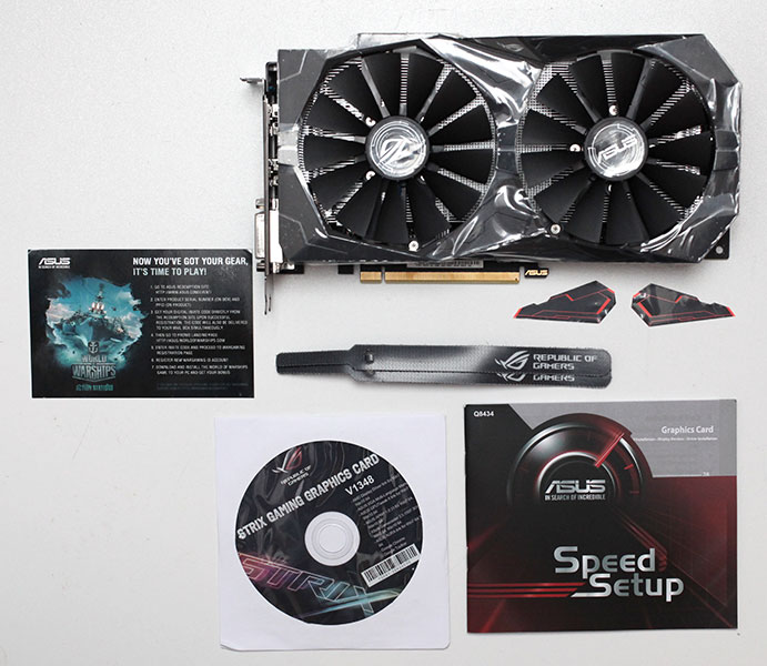
You will receive:
- Graphics card
- Driver CD + documentation
- ASUS zip ties
- ASUS stickers
- World of Warships coupon
The Card


ASUS has engineered a completely new cooler for their RX 470. It is dominated by plastic and has no colored highlights. Some stickers are included in the package, so you can put them on if you prefer some color instead of the all-black theme. Dimensions of the card are 24.5 cm x 13.0 cm.
Installation requires two slots in your system.
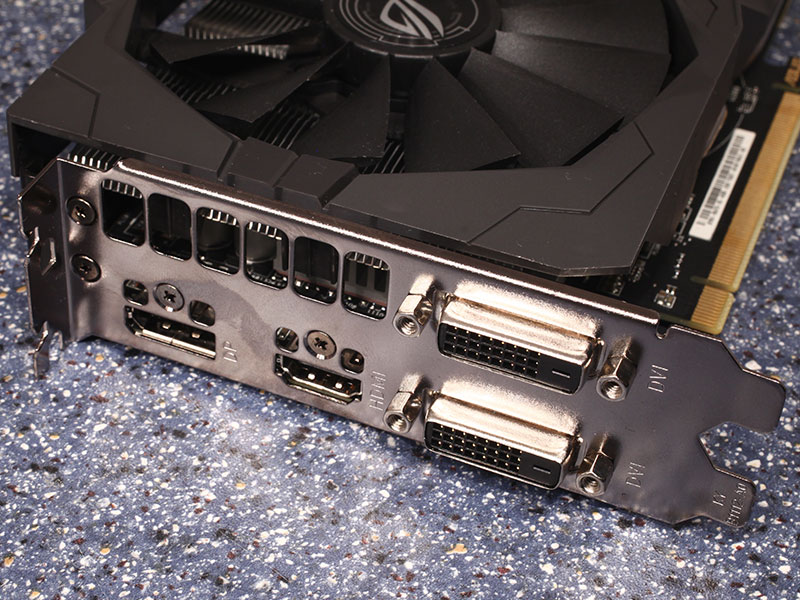
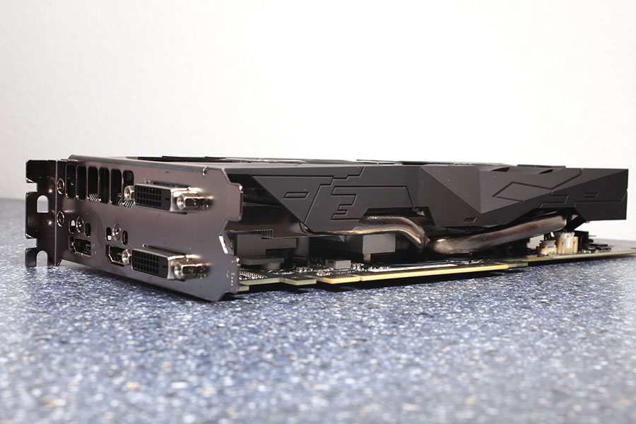
Display connectivity options include two DVI ports, one HDMI port, and one DisplayPort.
The HDMI port is now version 2.0b, and DisplayPort has been updated to 1.3 HBR3/1.4 HDR ready, which enables support for 4K @ 120 Hz and 5K @ 60 Hz, or 8K @ 60 Hz with two cables. GPU accelerated encoding is now supported for H.264 at up to 4K30, and HEVC is supported at up to 4K60. Accelerated decoding is supported for HEVC at up to 4K60 Main-10, VP9 is supported at up to 4K, and H.264 works at up to 4K120.
AMD CrossFire has been running over the PCI-Express bus for a few generations now. The Polaris Series is no different.
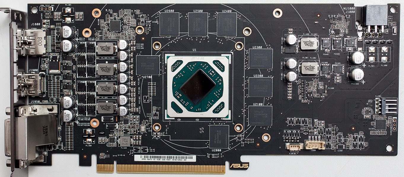
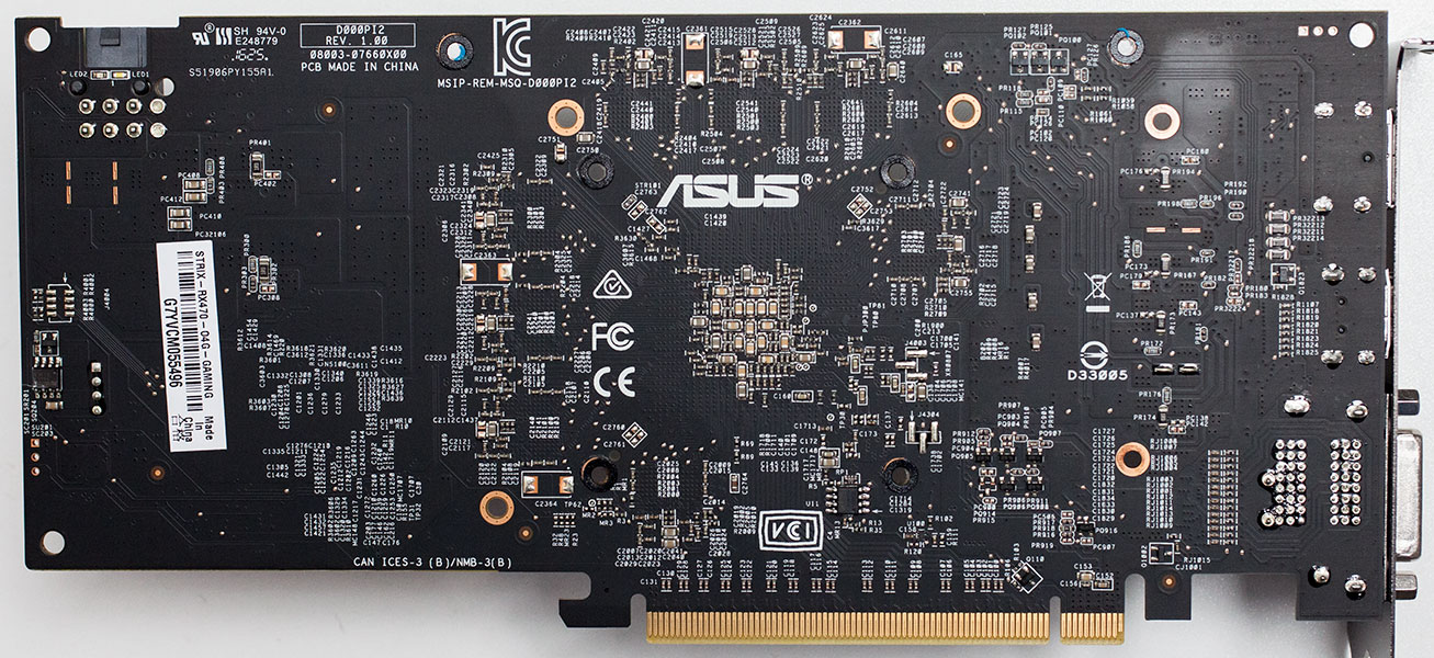
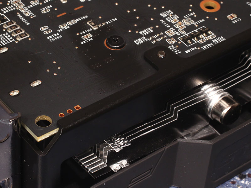
Pictured above are the front and back, showing the disassembled board. High-res versions are also available (front, back).
Our Patreon Silver Supporters can read articles in single-page format.
Apr 24th, 2025 08:27 EDT
change timezone
Latest GPU Drivers
New Forum Posts
- To distill or not distill what say ye? (77)
- RX 9000 series GPU Owners Club (508)
- Are the 8 GB cards worth it? (127)
- Throttlestop 9.7.3 Legion 7 Pro 13900HX, RTX4090 locking frequency issue (3)
- What's your latest tech purchase? (23586)
- random system shutdown with fans running at full speed (57)
- The TPU UK Clubhouse (26166)
- White Taichi 7900XTX (12)
- Help Needed with 100% SSD Usage and PC Stuttering (4)
- GameTechBench GPU benchmark is already out! (350)
Popular Reviews
- NVIDIA GeForce RTX 5060 Ti 8 GB Review - So Many Compromises
- Colorful iGame B860M Ultra V20 Review
- ASUS GeForce RTX 5060 Ti TUF OC 16 GB Review
- ASRock X870E Taichi Lite Review
- Upcoming Hardware Launches 2025 (Updated Apr 2025)
- Sapphire Radeon RX 9070 XT Pulse Review
- Sapphire Radeon RX 9070 XT Nitro+ Review - Beating NVIDIA
- NVIDIA GeForce RTX 5060 Ti PCI-Express x8 Scaling
- AMD Ryzen 7 9800X3D Review - The Best Gaming Processor
- ASUS GeForce RTX 5080 TUF OC Review
Controversial News Posts
- NVIDIA GeForce RTX 5060 Ti 16 GB SKU Likely Launching at $499, According to Supply Chain Leak (182)
- NVIDIA Sends MSRP Numbers to Partners: GeForce RTX 5060 Ti 8 GB at $379, RTX 5060 Ti 16 GB at $429 (127)
- NVIDIA Launches GeForce RTX 5060 Series, Beginning with RTX 5060 Ti This Week (115)
- Nintendo Confirms That Switch 2 Joy-Cons Will Not Utilize Hall Effect Stick Technology (105)
- Nintendo Switch 2 Launches June 5 at $449.99 with New Hardware and Games (99)
- Sony Increases the PS5 Pricing in EMEA and ANZ by Around 25 Percent (85)
- NVIDIA PhysX and Flow Made Fully Open-Source (77)
- Windows Notepad Gets Microsoft Copilot Integration (75)