 29
29
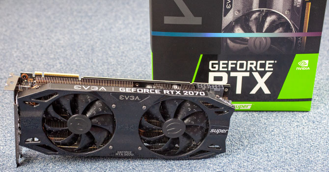
EVGA GeForce RTX 2070 Super KO Review
(29 Comments) »Introduction
Today, we review the EVGA GeForce RTX 2070 Super KO, EVGA's most affordable RTX 2070 Super graphics card priced at $499. However, EVGA already had a $499 RTX 2070 Super, the RTX 2070 Super Black, which just like the KO sticks to NVIDIA-reference clock speeds, lacks a backplate, and offers idle fan stop to one-up NVIDIA's Founders Edition card. So where did the KO come from?
The story begins with the Radeon RX 5600 XT. Through a last-minute specs update, AMD managed to get its $279 RX 5600 XT to launch with performance matching the then $349 GeForce RTX 2060. This turned up the heat on NVIDIA, and they decided to allow a design that uses a cost-efficient GTX 1660 Ti PCB paired with the RTX 2060 GPU. That product was the $299 EVGA RTX 2060 KO, a resurrection of the KO brand extension which was able to thwart the RX 5600 XT wherever it was available, so EVGA's designers could save the day for NVIDIA and go home for a pint. However, EVGA didn't rest. Earlier this month, it launched the GeForce GTX 2070 Super and RTX 2080 Super KO graphics cards, which raised our eyebrows.
The EVGA RTX 2070 Super KO we have with us launches at $510 officially, with an instant online discount that makes it a $499 product. The EVGA RTX 2070 Super Black, which was until now being sold at a "discounted" $499, is back to its original $510 online price. What does the $10 account for? All that sets the KO apart from the Black is the lack of the USB type-C VirtualLink connector on the KO. That's it.
NVIDIA designed the GeForce RTX 2070 Super to be the gateway to its high-end graphics segment. Based on the 12 nm "TU104" silicon, it features 2,560 TMUs, 160 TMUs, 64 ROPs, and a 256-bit wide GDDR6 memory interface holding 8 GB of memory that ticks at 14 Gbps. The GPU runs at up to 1770 MHz GPU Boost and 1605 MHz nominal, which are the same speeds the EVGA KO ships with. Among its display connectors are three DisplayPorts and one HDMI. In this review, we take the RTX 2070 Super KO for a spin to find out if you need to spend any more than $499 to knock high-resolution AAA gaming out.
| Price | Shader Units | ROPs | Core Clock | Boost Clock | Memory Clock | GPU | Transistors | Memory | |
|---|---|---|---|---|---|---|---|---|---|
| RX 5600 XT | $270 | 2304 | 64 | 1375 MHz | 1560 MHz | 1500 MHz | Navi 10 | 10300M | 6 GB, GDDR6, 192-bit |
| RTX 2060 | $300 | 1920 | 48 | 1365 MHz | 1680 MHz | 1750 MHz | TU106 | 10800M | 6 GB, GDDR6, 192-bit |
| RX 5700 | $320 | 2304 | 64 | 1465 MHz | 1625 MHz | 1750 MHz | Navi 10 | 10300M | 8 GB, GDDR6, 256-bit |
| GTX 1080 | $500 | 2560 | 64 | 1607 MHz | 1733 MHz | 1251 MHz | GP104 | 7200M | 8 GB, GDDR5X, 256-bit |
| RTX 2060 Super | $400 | 2176 | 64 | 1470 MHz | 1650 MHz | 1750 MHz | TU106 | 10800M | 8 GB, GDDR6, 256-bit |
| RX Vega 64 | $390 | 4096 | 64 | 1247 MHz | 1546 MHz | 953 MHz | Vega 10 | 12500M | 8 GB, HBM2, 2048-bit |
| GTX 1080 Ti | $700 | 3584 | 88 | 1481 MHz | 1582 MHz | 1376 MHz | GP102 | 12000M | 11 GB, GDDR5X, 352-bit |
| RX 5700 XT | $380 | 2560 | 64 | 1605 MHz | 1755 MHz | 1750 MHz | Navi 10 | 10300M | 8 GB, GDDR6, 256-bit |
| RTX 2070 | $400 | 2304 | 64 | 1410 MHz | 1620 MHz | 1750 MHz | TU106 | 10800M | 8 GB, GDDR6, 256-bit |
| RTX 2070 Super | $500 | 2560 | 64 | 1605 MHz | 1770 MHz | 1750 MHz | TU104 | 13600M | 8 GB, GDDR6, 256-bit |
| EVGA RTX 2070 Super KO | $500 | 2560 | 64 | 1605 MHz | 1770 MHz | 1750 MHz | TU104 | 13600M | 8 GB, GDDR6, 256-bit |
| Radeon VII | $600 | 3840 | 64 | 1802 MHz | N/A | 1000 MHz | Vega 20 | 13230M | 16 GB, HBM2, 4096-bit |
| RTX 2080 | $630 | 2944 | 64 | 1515 MHz | 1710 MHz | 1750 MHz | TU104 | 13600M | 8 GB, GDDR6, 256-bit |
| RTX 2080 Super | $700 | 3072 | 64 | 1650 MHz | 1815 MHz | 1940 MHz | TU104 | 13600M | 8 GB, GDDR6, 256-bit |
| RTX 2080 Ti | $1080 | 4352 | 64 | 1350 MHz | 1545 MHz | 1750 MHz | TU102 | 18600M | 11 GB, GDDR6, 352-bit |
Packaging


The Card


EVGA's card looks very similar visually to the company's other Turing cards. A backplate is not included.
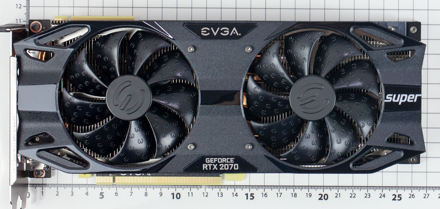
Dimensions of the card are 26 x 11.5 cm.


Installation requires two slots in your system.

Display connectivity options include three standard DisplayPort 1.4a and an HDMI 2.0b.
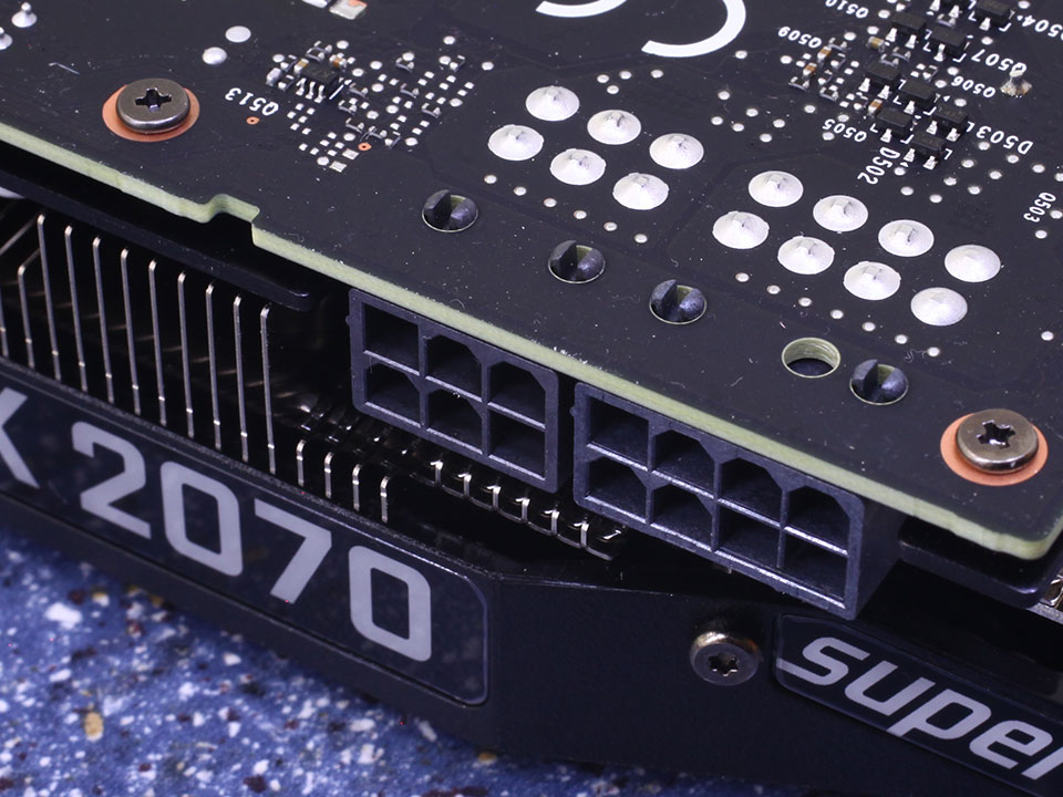
The board uses one 8-pin and one 6-pin power connector. This input configuration is specified for up to 375 watts of power draw.

With Turing, NVIDIA is using NVLink as a physical layer for its next-generation SLI technology. NVLink provides sufficient bandwidth for multi-GPU rendering at 8K 60 Hz, 4K 120 Hz, and other such bandwidth-heavy display resolutions. It's a point-to-point link between your GPUs, so latencies will be lower compared to pushing data through the PCI-Express bus.
Disassembly

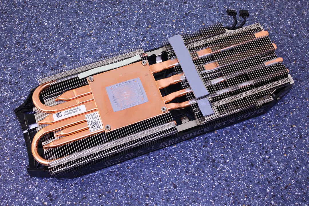
EVGA is using six heatpipes on their thermal solution, which is paired with a copper base to maximize heat transfer. This piece of the cooler also provides cooling for parts of the VRM circuitry.


Once the main heatsink is removed, a second metal plate becomes visible, which provides cooling for the memory chips and VRM circuitry.
High-resolution PCB Pictures
These pictures are for the convenience of volt modders and people who would like to see all the finer details on the PCB. Feel free to link back to us and use these in your articles or forum posts.
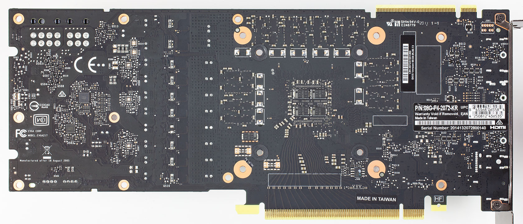
High-res versions are also available (front, back).
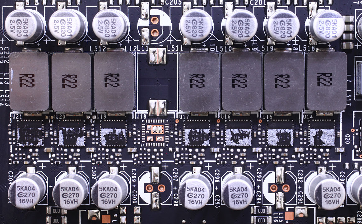
Circuit Board (PCB) Analysis
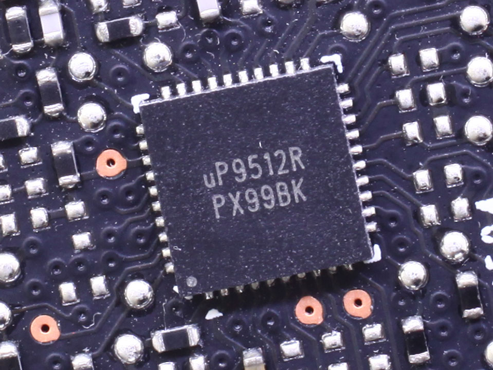
The GPU VRM is a 7-phase setup controlled by a UPI uP9512R controller.
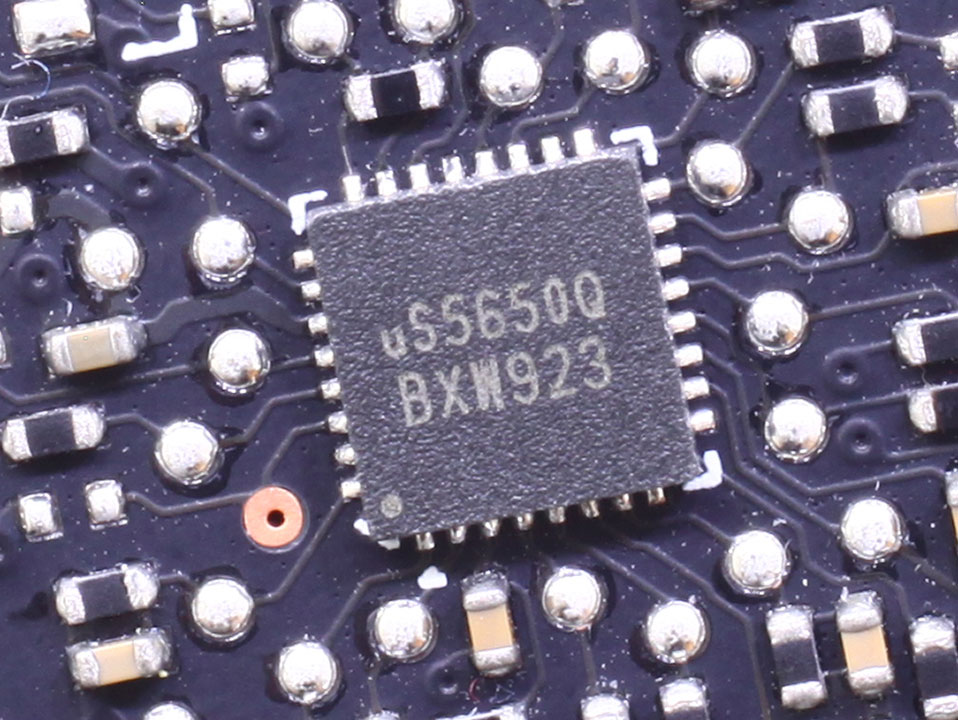
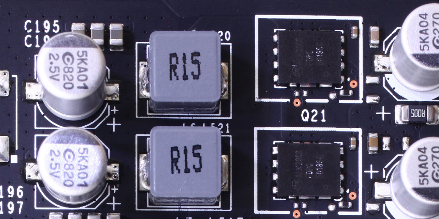
The memory VRM is dual-phase and managed by a UPI uS5650Q controller—a fairly new design.
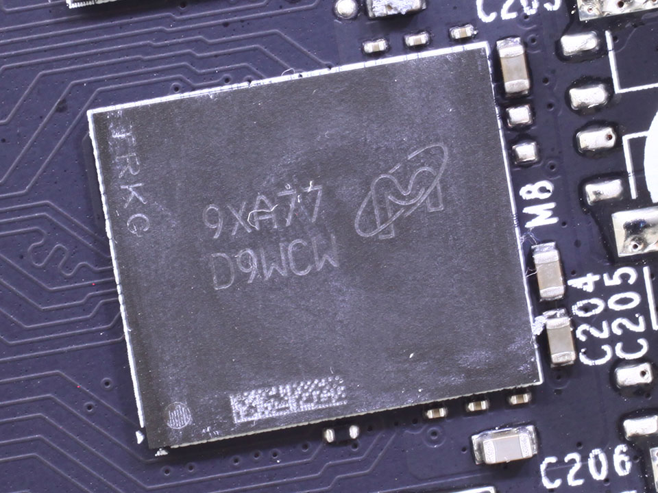
The GDDR6 memory chips are made by Micron and carry the model number D9WCW, which decodes to MT61K256M32JE-14:A. They are specified to run at 1750 MHz (14 Gbps GDDR6 effective).

NVIDIA's TU104 graphics processor is the company's second-largest chip using the Turing architecture. It is produced on a 12 nm process at TSMC, Taiwan and has a transistor count of 13.6 billion with a die size of 545 mm².
Our Patreon Silver Supporters can read articles in single-page format.
Apr 24th, 2025 12:09 EDT
change timezone
Latest GPU Drivers
New Forum Posts
- Help in overclocking the AMD Ryzen 7 7700 in ASUS TUF B650-PLUS WiFi Mobo (3)
- I dont understand the phone OS world..... (25)
- Current Sales, Bundles, Giveaways (10323)
- Are the 8 GB cards worth it? (155)
- Free Games Thread (4645)
- Throttlestop 9.7.3 Legion 7 Pro 13900HX, RTX4090 locking frequency issue (4)
- To distill or not distill what say ye? (95)
- The TPU UK Clubhouse (26170)
- New GPU 5070 Ti or better CPU Ryzen7 7800X3D ? (16)
- TPU's Nostalgic Hardware Club (20275)
Popular Reviews
- NVIDIA GeForce RTX 5060 Ti 8 GB Review - So Many Compromises
- Colorful iGame B860M Ultra V20 Review
- ASUS GeForce RTX 5060 Ti TUF OC 16 GB Review
- ASRock X870E Taichi Lite Review
- Upcoming Hardware Launches 2025 (Updated Apr 2025)
- Sapphire Radeon RX 9070 XT Pulse Review
- Sapphire Radeon RX 9070 XT Nitro+ Review - Beating NVIDIA
- NVIDIA GeForce RTX 5060 Ti PCI-Express x8 Scaling
- AMD Ryzen 7 9800X3D Review - The Best Gaming Processor
- ASUS GeForce RTX 5080 TUF OC Review
Controversial News Posts
- NVIDIA GeForce RTX 5060 Ti 16 GB SKU Likely Launching at $499, According to Supply Chain Leak (182)
- NVIDIA Sends MSRP Numbers to Partners: GeForce RTX 5060 Ti 8 GB at $379, RTX 5060 Ti 16 GB at $429 (127)
- NVIDIA Launches GeForce RTX 5060 Series, Beginning with RTX 5060 Ti This Week (115)
- Nintendo Confirms That Switch 2 Joy-Cons Will Not Utilize Hall Effect Stick Technology (105)
- Nintendo Switch 2 Launches June 5 at $449.99 with New Hardware and Games (99)
- Sony Increases the PS5 Pricing in EMEA and ANZ by Around 25 Percent (85)
- NVIDIA PhysX and Flow Made Fully Open-Source (77)
- Windows Notepad Gets Microsoft Copilot Integration (75)