 210
210
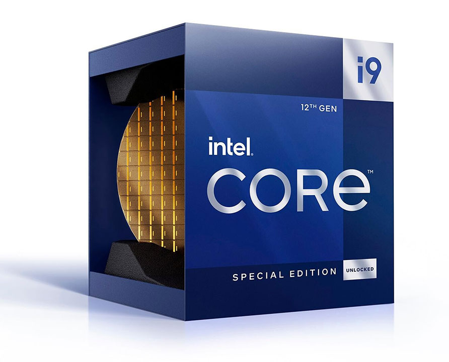
Intel Core i9-12900KS Review - The Best Just Got Better
(210 Comments) »Introduction
In case you're wondering, this is a proper review, not an April Fools' prank.
The Core i9-12900KS "Alder Lake" is a Special Edition processor SKU by Intel positioned at the very top of its desktop processor lineup. Intel has been doing such unconventional releases for the past few generations, including the Core i7-8086K and Core i9-9900KS. There were no such SKUs in the 10th and 11th generations, probably because Intel felt AMD had an unassailable performance lead both in gaming and productivity performance at the time. We're still in the thick of the golden era of PC processor competition between Intel and AMD with Ryzen and Core trying to win over the hearts of users.
Intel already holds the gaming performance crown with the Core i9-12900K, and its multi-threaded productivity performance is right in the league of 12-core and 16-core Ryzen 9 5000 "Zen 3" processors. What probably pushed Intel to come up with the i9-12900KS is AMD's June 2021 announcement of the 3D Vertical Cache technology followed by January 2022 claims that the new Ryzen 7 5800X3D, the first processor with this tech, is the "world's best gaming processor," catching up to the i9-12900K in gaming despite being based on the old "Zen 3" architecture and DDR4. Of course, Intel's response was to cook up a faster version of the i9-12900K, and we hence have the i9-12900KS for review today.

Architecturally and feature-wise, the Core i9-12900KS is mostly identical to the i9-12900K. You get eight "Golden Cove" performance cores (or P-cores), eight efficiency cores (or E-cores), 30 MB of shared L3 cache, an Xe LP iGPU with 32 EUs, and next-generation I/O that features PCI-Express Gen 5 and DDR5 memory while maintaining backwards-compatibility with DDR4. The higher-clocked P-cores are new, and these impact gaming performance. The P-cores now come with a maximum boost frequency of 5.50 GHz instead of the 5.20 GHz on the i9-12900K.
This is achieved with the re-introduction of the Thermal Velocity Boost feature that was rudimentary in the i9-12900K. The "KS" has a P-core base frequency of 3.40 GHz, which is 3.20 GHz on the i9-12900K. Turbo Boost 2.0 is 100 MHz higher at 5.20 GHz vs. 5.10 GHz. Turbo Boost Max 3.0 is again 100 MHz higher, at 5.30 GHz vs. 5.20 GHz. 5.20 GHz is where the i9-12900K topped out at stock settings. The i9-12900KS leverages Thermal Velocity Boost to push the P-core frequency up to 5.50 GHz. This algorithm works in the same manner as on the i9-11900K or i9-10900K, by rewarding good CPU cooling with those extra turbo bins. The E-core base and turbo frequencies get a 100 MHz uplift, too. iGPU clock speeds are unchanged. These higher clock speeds come at a slight increase in the processor base power (PBP) value, which is now 150 W compared to 125 W on the i9-12900K. The maximum turbo power (MTP), however, is identical between the two chips, at 241 W. Just like the Core i9-12900K, the 12900KS runs at PL1=PL2=241 W.
Besides Thermal Velocity Boost, the Intel Adaptive Boost Technology (ABT) makes a comeback. ABT was introduced with the i9-11900K "Rocket Lake," but was not included with the i9-12900K. ABT opportunistically enables additional boost frequency bins across all P-cores, improving multi-threaded performance.
As mentioned earlier, the Core i9-12900KS is a "Special Edition" SKU. Its retail availability won't be as widespread as the i9-12900K. Intel is pricing the chip at US$739 for 1K quantities, a $140 premium over the i9-12900K. We're using a $750 price point for calculations in this review. In return, you're promised the "world's fastest desktop processor." We're here to find out if that's the case.
| Price | Cores / Threads | Base Clock | Max. Boost | L3 Cache | TDP | Architecture | Process | Socket | |
|---|---|---|---|---|---|---|---|---|---|
| Core i7-9700K | $310 | 8 / 8 | 3.6 GHz | 4.9 GHz | 12 MB | 95 W | Coffee Lake | 14 nm | LGA 1151 |
| Core i7-10700K | $325 | 8 / 16 | 3.8 GHz | 5.1 GHz | 16 MB | 125 W | Comet Lake | 14 nm | LGA 1200 |
| Core i7-11700K | $315 | 8 / 16 | 3.6 GHz | 5.0 GHz | 16 MB | 125 W | Rocket Lake | 14 nm | LGA 1200 |
| Ryzen 7 3700X | $320 | 8 / 16 | 3.6 GHz | 4.4 GHz | 32 MB | 65 W | Zen 2 | 7 nm | AM4 |
| Ryzen 7 5700G | $350 | 8 / 16 | 3.8 GHz | 4.6 GHz | 16 MB | 65 W | Zen 3 + Vega | 7 nm | AM4 |
| Core i7-12700K | $385 | 8+4 / 20 | 3.6 / 2.7 GHz | 5.0 / 3.8 GHz | 25 MB | 125 W | Alder Lake | 10 nm | LGA 1700 |
| Ryzen 7 5800X | $350 | 8 / 16 | 3.8 GHz | 4.7 GHz | 32 MB | 105 W | Zen 3 | 7 nm | AM4 |
| Core i9-10900 | $440 | 10 / 20 | 2.8 GHz | 5.2 GHz | 20 MB | 65 W | Comet Lake | 14 nm | LGA 1200 |
| Ryzen 9 3900X | $490 | 12 / 24 | 3.8 GHz | 4.6 GHz | 64 MB | 105 W | Zen 2 | 7 nm | AM4 |
| Ryzen 9 5900X | $450 | 12 / 24 | 3.7 GHz | 4.8 GHz | 64 MB | 105 W | Zen 3 | 7 nm | AM4 |
| Core i9-9900K | $470 | 8 / 16 | 3.6 GHz | 5.0 GHz | 16 MB | 95 W | Coffee Lake | 14 nm | LGA 1151 |
| Core i9-10900K | $390 | 10 / 20 | 3.7 GHz | 5.3 GHz | 20 MB | 125 W | Comet Lake | 14 nm | LGA 1200 |
| Core i9-11900K | $405 | 8 / 16 | 3.5 GHz | 5.3 GHz | 16 MB | 125 W | Rocket Lake | 14 nm | LGA 1200 |
| Ryzen 9 3950X | $765 | 16 / 32 | 3.5 GHz | 4.7 GHz | 64 MB | 105 W | Zen 2 | 7 nm | AM4 |
| Ryzen 9 5950X | $670 | 16 / 32 | 3.4 GHz | 4.9 GHz | 64 MB | 105 W | Zen 3 | 7 nm | AM4 |
| Core i9-12900K | $600 | 8+8 / 24 | 3.2 / 2.4 GHz | 5.2 / 3.9 GHz | 30 MB | 125 W | Alder Lake | 10 nm | LGA 1700 |
| Core i9-12900KS | $750 | 8+8 / 24 | 3.4 / 2.5 GHz | 5.5 / 4.0 GHz | 30 MB | 150 W | Alder Lake | 10 nm | LGA 1700 |


Intel paper-launched the 12th Gen Core processor family on October 27, allowing us to post everything about the processor except performance testing, so we did a more comprehensive preview article on the "Alder Lake" microarchitecture. "Alder Lake-S" is the first desktop processor silicon built by Intel on its Intel 7 silicon fabrication node, formerly known as 10 nm Enhanced SuperFin. This node offers comparable transistor-density and power characteristics as 7 nm-class nodes by TSMC. The die measures approximately 200 mm², although it is noticeably smaller than the 14 nm "Rocket Lake-S" die.


The monolithic silicon features 8 "Golden Cove" P-cores and 8 "Gracemont" E-cores. The E-cores are spread across two 4-core "E-core clusters." A bi-directional Ringbus and 30 MB of L3 cache connect the P-cores, and E-core clusters, with the Uncore (integrated northbridge) and iGPU. The chip features a dual-mode memory controller that supports 160-bit wide DDR5 (native support for DDR5-4800) or 128-bit wide DDR4 (native support for DDR4-3200). The Gen12 Xe LP iGPU is almost the same as on the "Rocket Lake-S" silicon, with only a minor speed bump. The PCI-Express root complex is fascinating. The silicon puts out 16 Gen 5 lanes, 32 Gbps per lane, which are allocated to the PEG slot on the motherboard, and 12 Gen 4 lanes, 16 Gbps per lane, of which four drive a CPU-attached M.2 NVMe slot and eight serve as a physical layer of the DMI 4.0 x8 chipset bus, which is 128 Gbps per direction bandwidth.

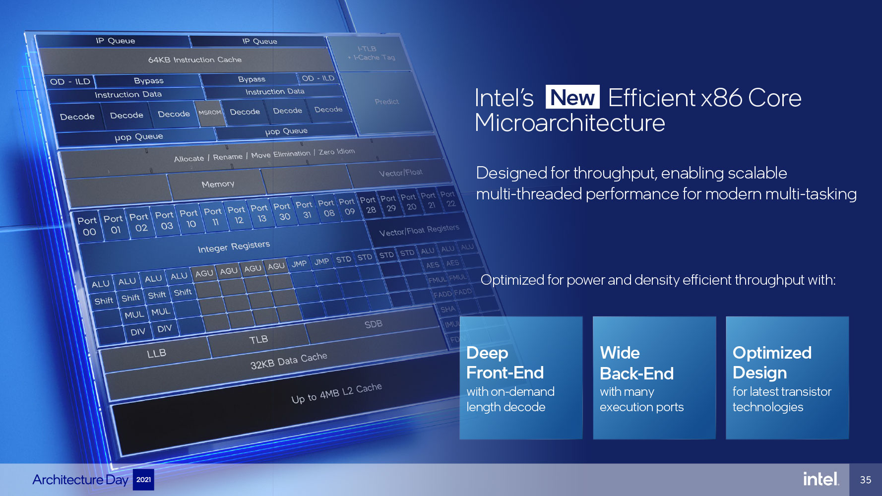
The "Golden Cove" performance core (P-core) features numerical increments to the decode unit, micro-op queue, and micro-op cache. The out-of-order (OoO) engine sees similar increments with 6-wide allocation and 12-wide execution ports, compared to 5-wide allocation and 10-wide execution ports for Cypress Cove. The execution stage sees the addition of a fifth execution port and ALU, FMA with FP16 support, and an updated fast adder (FADD). Similar improvements are made to the cache and memory sub-system. These add toward the 28% IPC uplift for this core. The E-core, on the other hand, is designed to provide a massive performance uplift from the previous-generation "Tremont" low-power microarchitecture, mainly to give it certain ISA capabilities found in larger cores, such as AVX2. The front-end is upgraded by a double-size 64 KB L1 instruction cache, more powerful branch-prediction unit, and two sets of triple out-of-order decoders. The out-of-order engine features a wide 256-entry OoO window and 17 execution ports for more parallelism. The execution stage sees a near 33% increase in both scalar and vector execution stages, as well as double the load store.
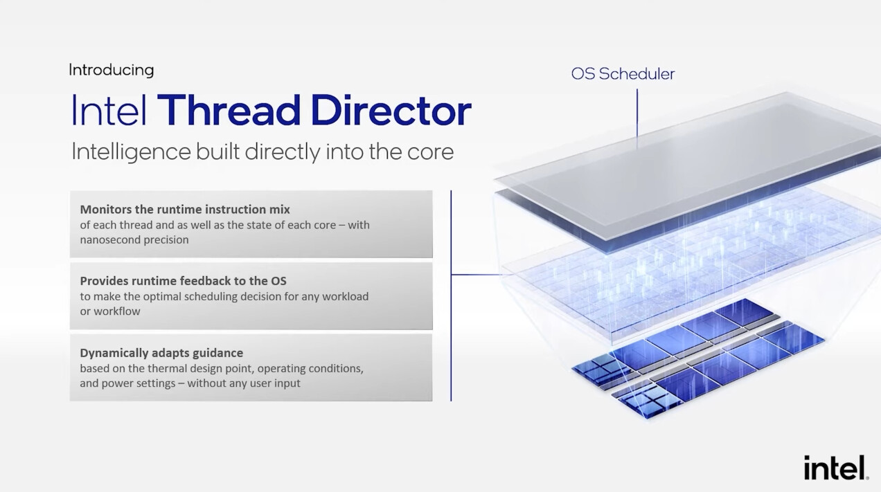

Intel Thread Director is a vital component that ensures the operating system doesn't see "Alder Lake" as having the same kind of CPU cores, sending processing traffic uniformly to all cores. Instead, it gives the OS a degree of awareness of the Hybrid architecture and ensures certain kinds of tasks are allocated exclusively on P-cores and others on E-cores. It also senses the nature of the processing workload, whether it's running in the foreground or background, and decides which kind of cores to tie it to. The OS scheduler by itself moves traffic between cores to meet certain power and thermal objectives, but Thread Director ensures this movement doesn't break the core-type hierarchy. Windows 11 is the recommended version of Windows for Alder Lake as it introduces the ability for software to inform the processor of the nature of its work, and the kind of cores it's comfortable getting processed by.


To eke out the best-possible thermals from the 14 nm node it was stuck with, Intel pulled off some innovative ways to transfer heat between the silicon and cooling solution over the past couple of solutions. These innovations continue with Alder Lake. The die and STIM are now thinner, and the copper IHS thicker. Among the new overclocking capabilities are the ability to tweak even the E-cores, DDR5 memory, new XMP 3.0 profiles for DDR5 memory, synthetic BCLK that ensures a base-clock overclock doesn't break sensitive clock domains that rely on it, and external clock generation, in addition to the processor's internal clock generator.

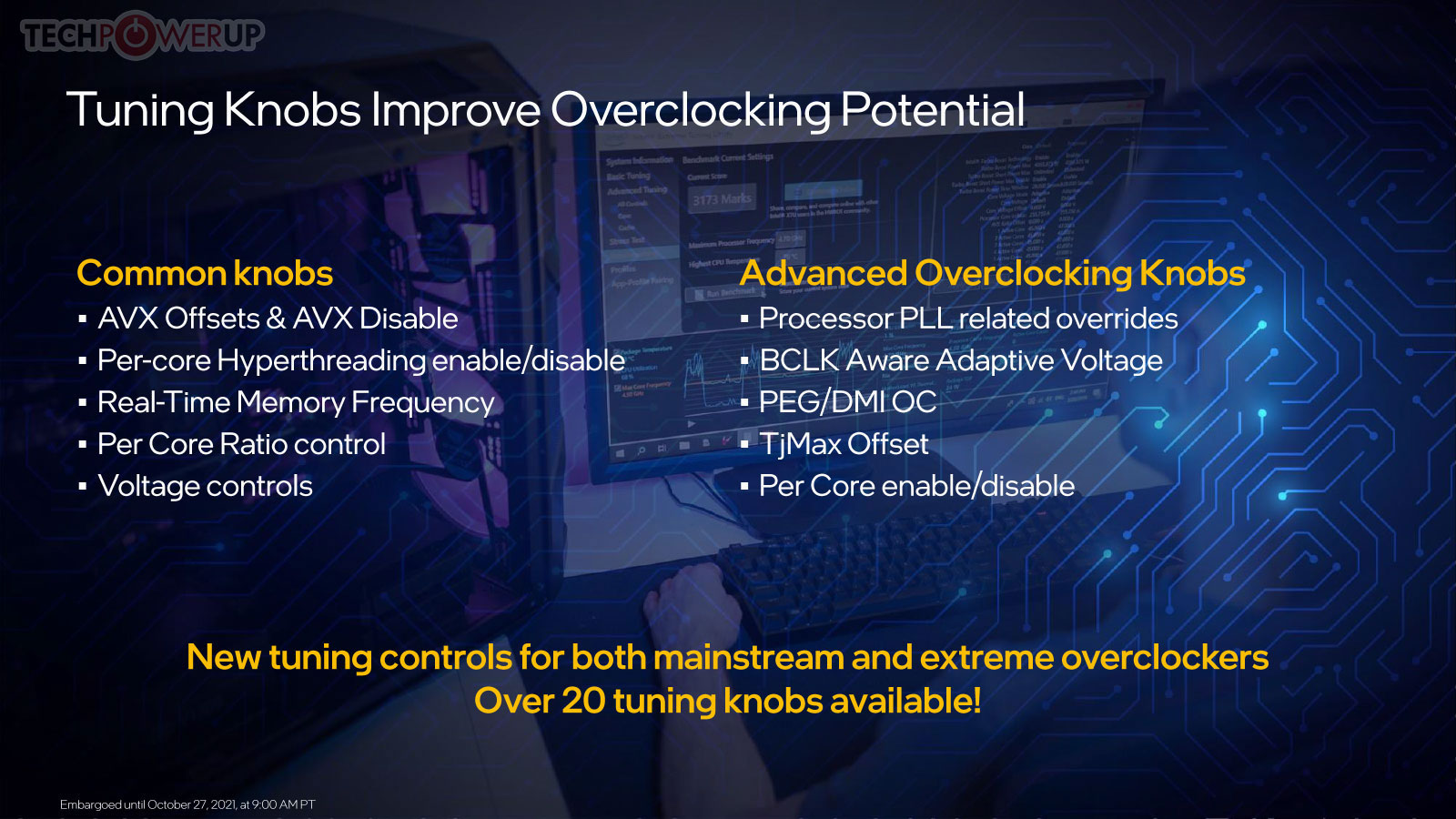
With the monolithic silicon gaining complexity, there are several new overclocking knobs and clock domains to maximize your overclock. The introduction of the E-core adds its own base-clock multiplier, called xE, which works separately from the core ratio of the P-cores, dubbed xP. The xG multiplier dictates iGPU frequency. xR dictates the frequency at which the Ringbus interconnect and L3 cache operate.
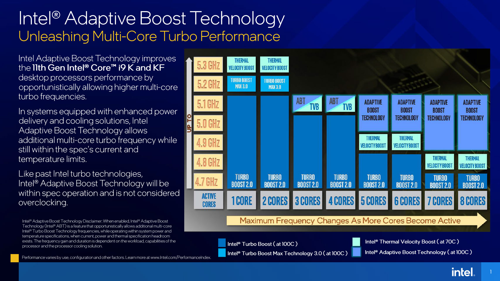
Intel Adaptive Boost Technology (ABT) is a new feature exclusive to the Core i9-12900KS in the 12th Generation, which works to significantly improve multi-threaded performance. To understand ABT, you'll have to understand the three frequency boosting technologies already available to these processors. The i9-12900KS features a nominal clock speed of 3.40 GHz. When all the P-cores are stressed, the chip can afford an all-core boost frequency of 4.80 GHz, provided factors such as the workload being non-AVX, the chip not having exhausted its power level time, etc. Classic Turbo Boost 2.0 drives frequencies up to 5.10 GHz on lighter workloads, for all the cores. Turbo Boost Max 3.0 adds another bin for two of the processor's favored (best-performing) cores, running them at 5.20 GHz. If the cooling performance checks out, Thermal Velocity Boost adds the final 100 MHz to the favored cores, taking the frequency all the way up to 5.30 GHz.
Adaptive Boost is similar to ASUS's "Multi-core Enhancement"—it helps achieve higher clock frequencies when multiple CPU cores are loaded. Unlike the ASUS solution, which is brute-force and static, ABT takes into account not just power limits, thermals, and the cooling efficiency of your machine, but also your motherboard's CPU VRM solution. If the VRM is up for the job, additional power is drawn to elevate all the cores on the processor to higher boost states, improving performance for multi-threaded workloads. The above slide shows you exactly how much clock speed is added. The onus is on the motherboard vendors to design their products such that they can offer ABT, and the motherboard BIOS should report to the processor that its VRM can handle adaptive boosting. What makes ABT special is that it follows the CPU's clock-voltage curve, making it 100% crash-proof—it just works. The price you're paying is higher heat and power consumption. This feature sounds great, and throughout this review, we will test the performance impact of Adaptive Boost.
Intel Z690 Chipset
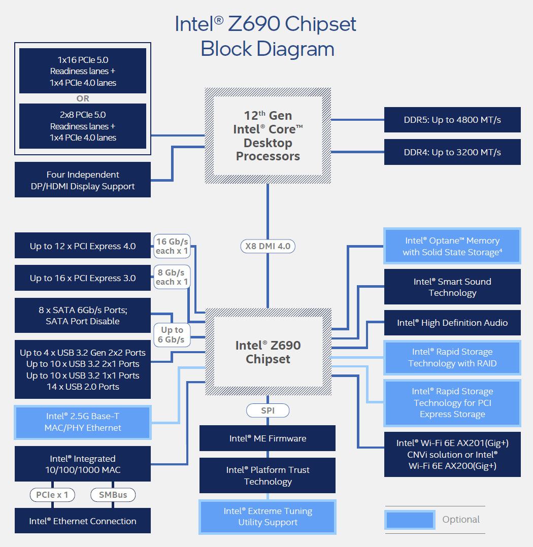
Intel debuted its 12th Gen Core desktop processors in 2021 exclusively with only the unlocked "K" and "KF" variants. As such, it only launched the companion Z690 chipset alongside those. The "locked" processor SKUs and value-ended chipsets joined the product stack in 2022. The Z690 chipset is Intel's first client chipset with PCI-Express 4.0 downstream connectivity. It talks to the "Alder Lake-S" processor over the DMI 4.0 x8 chipset bus. Downstream PCIe connectivity includes 12x Gen 4 and 16x Gen 3 PCIe general-purpose lanes. The rest of its chipset-attached connectivity is the same as Z590, including MIPI SoundWire support, NVMe RAID, 8-port SATA 6 Gbps, and recommended network interfaces that include 2.5 GbE and Wi-Fi 6E.
Intel B660 and H610 Chipsets

As of this writing, VERY few motherboards use the H670 client chipset, making the B660 Intel's mainstream desktop chipset for those with a "locked" 12th Gen Core processor the best option, those who don't need the I/O options of the Z690 and want to save big on the motherboard. The B660 lacks CPU overclocking support, but permits memory overclocking. Motherboard vendors can choose to give it a PCIe Gen 5 PEG slot, as well as DDR5 memory, although you may come across plenty of motherboards with PCIe Gen4 PEG and DDR4 memory. The B660 chipset uses a narrower 4-lane DMI 4.0 chipset bus than what 12th Gen Core processors are capable of (up to 8 DMI 4.0 lanes). This shouldn't be too much of a problem as the chipset only puts out 6 downstream PCIe Gen4 lanes, besides 8 Gen3 lanes. Motherboard designers should use the downstream Gen4 connectivity to wire out another M.2 Gen4 slot. You also get fewer high-bandwidth USB3 port types. The H610 is the bare entry-level chipset. You lose out on memory overclocking, only get Gen3 PCIe connectivity across the board, and have no CPU-attached NVMe.
Unboxing and Photography

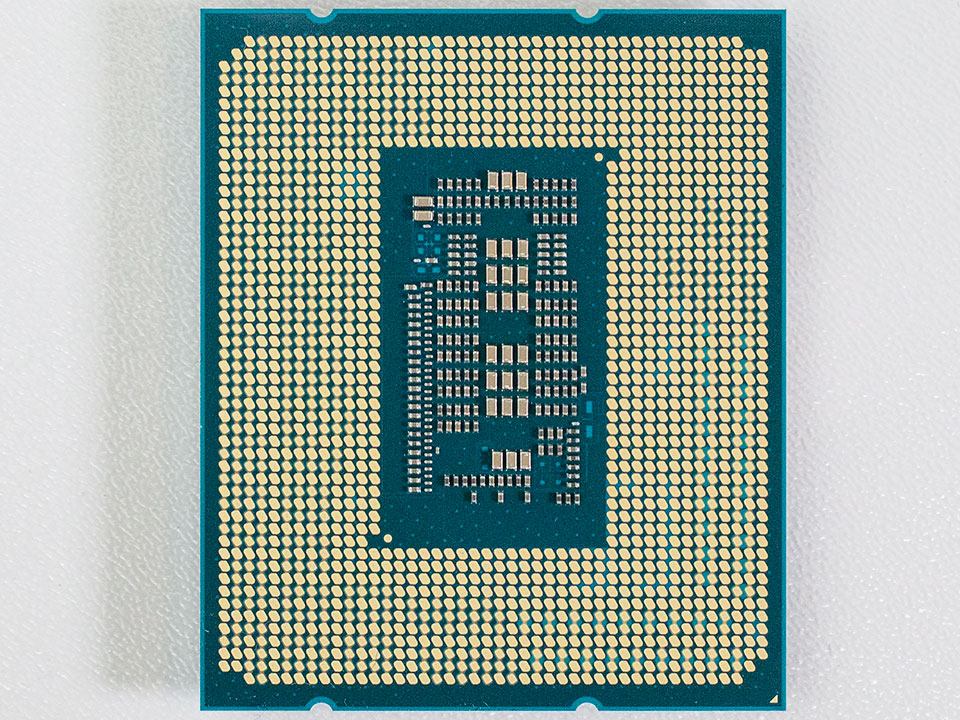
The Core i9-12900KS ships in a large box that contains only the processor (no cooler included). The CPU itself measures 37.5 mm x 45.0 mm and is a more rectangular-looking processor, much like the LGA1366 before it.
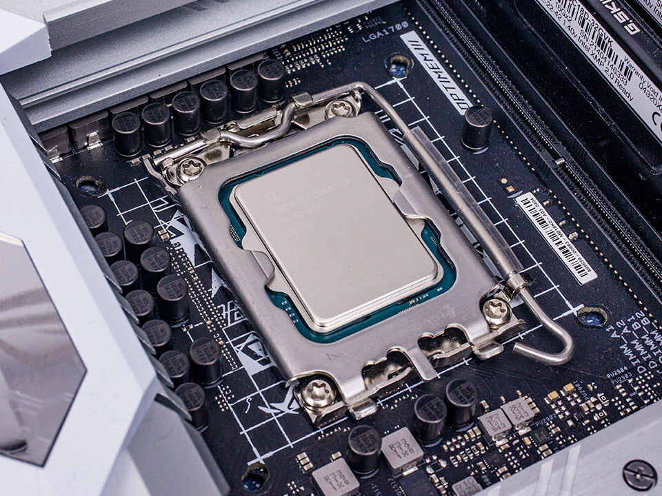
Intel Socket LGA1700 has an intuitive installation process that should be familiar from many past LGA sockets. Trouble is that it comes with a different cooler mount-hole spacing than LGA1200 and the five different Socket-H series sockets before it, so you'll need to search for a compatible cooler or get an updated mounting bracket.
Test Setup
- All applications, games, and processors are tested with the drivers and hardware listed below—no performance results were recycled between test systems.
- All games and applications are tested using the same version.
- All games are set to their highest quality setting unless indicated otherwise.
| Test System "Alder Lake" | |
|---|---|
| Processor: | All Intel 12th Generation processors |
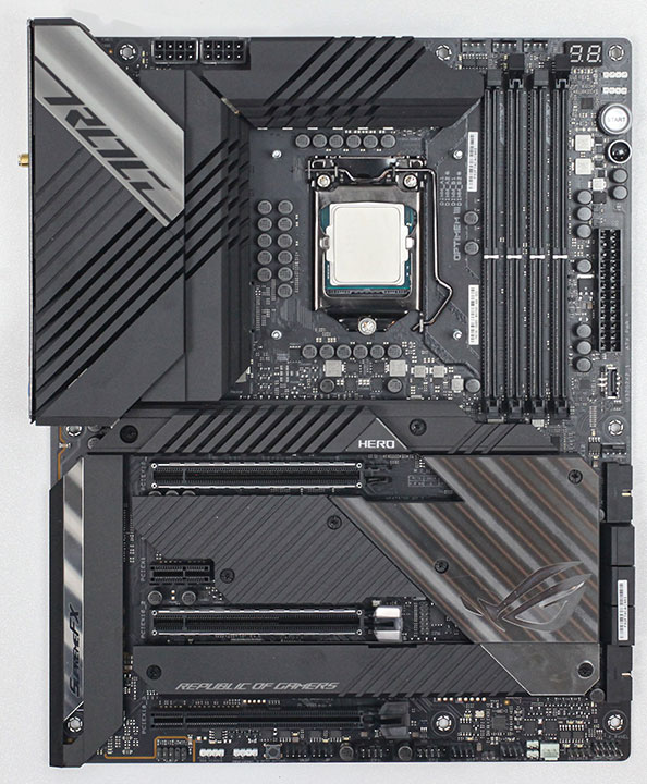
| Motherboard: | ASUS Z690 Maximus Hero / BIOS 0702 i9-12900KS: BIOS 1403 with 0x1F Microcode update for 12900KS |
| Memory: | 2x 16 GB G.SKILL Trident Z5 RGB DDR5-6000 36-36-36-76 2T / Gear 2 |
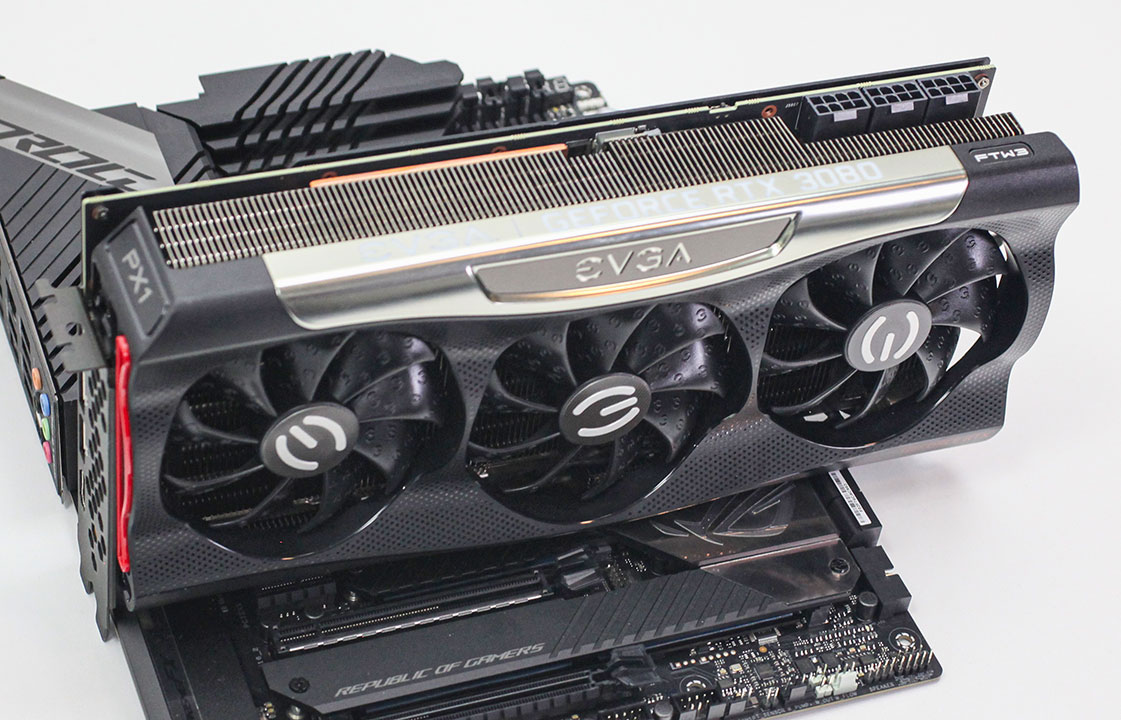
| Graphics: | EVGA GeForce RTX 3080 FTW3 Ultra |
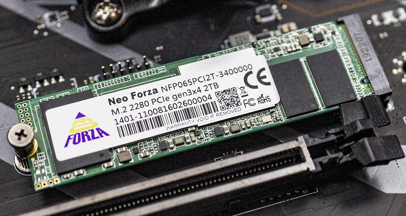
| Storage: | Neo Forza NFP065 1 TB M.2 NVMe SSD |
| Air Cooling: | Noctua NH-U14S |
| Water Cooling: | Arctic Liquid Freezer II 360 mm |
| Thermal Paste: | Arctic MX-5 |
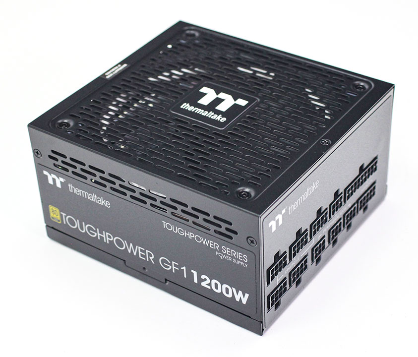
| Power Supply: | Thermaltake Toughpower GF1 1200 W |
| Software: | Windows 11 Professional 64-bit Build 10.0.22000.282 Includes AMD L3 latency fix |
| Drivers: | NVIDIA GeForce 496.49 WHQL |

| Test System "Zen 3" | |
|---|---|
| Processor: | All AMD Ryzen 5000 |
| Motherboard: | MSI MPG X570 Gaming Plus BIOS 7C37vAF3, AGESA 1.2.0.3c |
| Memory: | 2x 16 GB DDR4-3600 16-20-20-34 1T Infinity Fabric @ 1800 MHz 1:1 |
| All other specifications same as above | |
| Test System "Rocket Lake" | |
|---|---|
| Processor: | All Intel 11th Generation processors |
| Motherboard: | ASUS Z590 Maximus XIII Hero BIOS 1007 |
| Memory: | 2x 16 GB DDR4-3600 16-20-20-34 1T Gear 1 |
| All other specifications same as above | |
| Test System "Comet Lake" | |
|---|---|
| Processor: | All Intel 10th Generation processors |
| Motherboard: | ASUS Z490 Maximus XII Extreme BIOS 2301 |
| Memory: | 2x 16 GB DDR4-3600 16-20-20-34 1T |
| All other specifications same as above | |
Super Pi
SuperPi is one of the most popular benchmarks with overclockers and tweakers. It has been used in world-record competitions since forever. It is a purely single-threaded CPU test that calculates Pi to a large number of digits—32 million for our testing. Released in 1995, it only supports x86 floating-point instructions and thus makes for a good test for single-threaded legacy application performance.
Our Patreon Silver Supporters can read articles in single-page format.
Apr 14th, 2025 14:42 EDT
change timezone
Latest GPU Drivers
New Forum Posts
- Folding Pie and Milestones!! (9472)
- Your GPU history? (377)
- best ram to buy for my usage and system specs? (23)
- Advice on GPU upgrade (48)
- What's your latest tech purchase? (23549)
- Free Games Thread (4624)
- Gainward Phoenix RTX 5070ti Temperatures (5)
- Windows 11 Install/Change (2)
- Sapphire RX9070XT Nitro+ fan and high temperature problem (12)
- Help me identify Chip of this DDR4 RAM (10)
Popular Reviews
- TerraMaster F8 SSD Plus Review - Compact and quiet
- ASUS GeForce RTX 5080 TUF OC Review
- Thermaltake TR100 Review
- The Last Of Us Part 2 Performance Benchmark Review - 30 GPUs Compared
- Zotac GeForce RTX 5070 Ti Amp Extreme Review
- Sapphire Radeon RX 9070 XT Pulse Review
- Sapphire Radeon RX 9070 XT Nitro+ Review - Beating NVIDIA
- Upcoming Hardware Launches 2025 (Updated Apr 2025)
- MSI MAG CORELIQUID A15 360 Review
- AMD Ryzen 7 9800X3D Review - The Best Gaming Processor
Controversial News Posts
- NVIDIA GeForce RTX 5060 Ti 16 GB SKU Likely Launching at $499, According to Supply Chain Leak (182)
- NVIDIA Sends MSRP Numbers to Partners: GeForce RTX 5060 Ti 8 GB at $379, RTX 5060 Ti 16 GB at $429 (124)
- Nintendo Confirms That Switch 2 Joy-Cons Will Not Utilize Hall Effect Stick Technology (105)
- Over 200,000 Sold Radeon RX 9070 and RX 9070 XT GPUs? AMD Says No Number was Given (100)
- Nintendo Switch 2 Launches June 5 at $449.99 with New Hardware and Games (99)
- Sony Increases the PS5 Pricing in EMEA and ANZ by Around 25 Percent (79)
- NVIDIA PhysX and Flow Made Fully Open-Source (77)
- NVIDIA Pushes GeForce RTX 5060 Ti Launch to Mid-April, RTX 5060 to May (77)