 30
30
MSI GeForce RTX 4080 Super Expert Review
(30 Comments) »Introduction
The new MSI GeForce RTX 4080 Super Expert graphics card releasing today, introduces the company's latest attempt at an ultra-premium custom design tier. MSI is among the few NVIDIA board partners that's been making serious efforts to beat the NVIDIA Founders Edition in aesthetics and cooling performance. The new Expert brand sits alongside the company's SUPRIM X and SUPRIM Liquid tiers. It's also the first GeForce RTX product from the company to feature the MSI PRO logo that's usually found in notebooks, monitors, and pre-built desktops from the company targeted at the workstation and creator PC market segments. So the MSI RTX 4080 Super Expert is meant for the high-end gaming PC crowd that does quite a bit of creator work on the side, paired with NVIDIA's Studio drivers.
As for the GeForce RTX 4080 Super, it sits at the top of the Super series mid-lifecycle refresh of the RTX 40-series Ada. This refresh aims to being more performance at existing or lower price points. The RTX 4080 Super is recommended by NVIDIA for maxed out gaming at the 4K Ultra HD resolution, including with ray tracing. It is built on the same AD103 silicon as the original RTX 4080, but maxes it out, enabling all its available shaders. Perhaps the best aspect of the RTX 4080 Super isn't this increase in shaders, but a lowering in its MSRP to $1,000, from the $1,200 that the RTX 4080 launched at. This ensures that premium custom-design cards such as the MSI RTX 4080 Super Expert we're reviewing here, are priced similar to the original baseline price of the RTX 4080.

The GeForce RTX 4080 Super is being introduced to cement NVIDIA's competitive proposition against the AMD Radeon RX 7900 XTX, which can be often found around the $900 mark. The company probably felt that it didn't need to tap into the larger AD102 silicon driving the RTX 4090, to do this. Instead, the RTX 4080 Super enables all 80 SM physically present on the AD103, when compared to the RTX 4080 that nearly maxed it out with 76; and lower the baseline price of the resulting product by 20%. With 80 SM, the RTX 4080 Super enjoys some eye-pleasing counts of 10,240 CUDA cores, 320 Tensor cores, 80 RT cores, 320 TMUs, and 112 ROPs. The memory size is unchanged at 16 GB, across the chip's full 256-bit memory interface, cushioned by the 64 MB on-die cache; however NVIDIA has slightly increased the memory speed to 23 Gbps, over the 22.4 Gbps of the original RTX 4080. The Super refresh doesn't change the underlying Ada Lovelace graphics architecture, including its new CUDA cores that support shader execution reordering; new RT cores that support displaced micro-meshes that enable increase in complexity of ray traced objects; and optical flow accelerator, which enables the new DLSS 3 Frame Generation feature.
The MSI GeForce RTX 4080 Super Expert board design is perhaps the most truthful adaptation of the dual-axial flow-through cooler architecture introduced by NVIDIA with its past two generations of Founders Edition graphics cards. In fact, it takes the concept up a notch, and minimizes lateral ventilation from the sides of the card. There are two large fans on this triple-slot cooler; the first one is on the obverse side of the card, and toward the front end. It draws fresh air onto the heatsink underneath; which is ventilated from the cutouts in the rear I/O shield. The second fan is located on the reverse side, pulling air through the heatsink, through a large vent on the obverse side. The MSI Expert card also comes with factory overclocked speeds, with the GPU running at 2610 MHz boost frequency, compared to 2550 MHz reference. The company is pricing the card at $1150, a premium over the $1,000 baseline.
Short 10-Minute Video Comparing 9x RTX 4080 Super
Our goal with the videos is to create short summaries, not go into all the details and test results, which can be found in our written reviews.
| Price | Cores | ROPs | Core Clock | Boost Clock | Memory Clock | GPU | Transistors | Memory | |
|---|---|---|---|---|---|---|---|---|---|
| RX 6800 XT | $500 | 4608 | 128 | 2015 MHz | 2250 MHz | 2000 MHz | Navi 21 | 26800M | 16 GB, GDDR6, 256-bit |
| RTX 3080 | $450 | 8704 | 96 | 1440 MHz | 1710 MHz | 1188 MHz | GA102 | 28000M | 10 GB, GDDR6X, 320-bit |
| RTX 4070 | $540 | 5888 | 64 | 1920 MHz | 2475 MHz | 1313 MHz | AD104 | 35800M | 12 GB, GDDR6X, 192-bit |
| RX 7800 XT | $500 | 3840 | 96 | 2124 MHz | 2430 MHz | 2425 MHz | Navi 32 | 28100M | 16 GB, GDDR6, 256-bit |
| RX 6900 XT | $650 | 5120 | 128 | 2015 MHz | 2250 MHz | 2000 MHz | Navi 21 | 26800M | 16 GB, GDDR6, 256-bit |
| RX 6950 XT | $630 | 5120 | 128 | 2100 MHz | 2310 MHz | 2250 MHz | Navi 21 | 26800M | 16 GB, GDDR6, 256-bit |
| RTX 3090 | $800 | 10496 | 112 | 1395 MHz | 1695 MHz | 1219 MHz | GA102 | 28000M | 24 GB, GDDR6X, 384-bit |
| RTX 4070 Super | $600 | 7168 | 80 | 1980 MHz | 2475 MHz | 1313 MHz | AD104 | 35800M | 12 GB, GDDR6X, 192-bit |
| RTX 4070 Ti | $750 | 7680 | 80 | 2310 MHz | 2610 MHz | 1313 MHz | AD104 | 35800M | 12 GB, GDDR6X, 192-bit |
| RTX 4070 Ti Super | $800 | 8448 | 112 | 2340 MHz | 2610 MHz | 1313 MHz | AD103 | 45900M | 16 GB, GDDR6X, 256-bit |
| RX 7900 XT | $720 | 5376 | 192 | 2000 MHz | 2400 MHz | 2500 MHz | Navi 31 | 57700M | 20 GB, GDDR6, 320-bit |
| RTX 3090 Ti | $1050 | 10752 | 112 | 1560 MHz | 1950 MHz | 1313 MHz | GA102 | 28000M | 24 GB, GDDR6X, 384-bit |
| RTX 4080 | $1200 | 9728 | 112 | 2205 MHz | 2505 MHz | 1400 MHz | AD103 | 45900M | 16 GB, GDDR6X, 256-bit |
| RTX 4080 Super | $1000 | 10240 | 112 | 2295 MHz | 2550 MHz | 1438 MHz | AD103 | 45900M | 16 GB, GDDR6X, 256-bit |
| MSI RTX 4080 Super Expert | $1150 | 10240 | 112 | 2295 MHz | 2610 MHz | 1438 MHz | AD103 | 45900M | 16 GB, GDDR6X, 256-bit |
| RX 7900 XTX | $970 | 6144 | 192 | 2300 MHz | 2500 MHz | 2500 MHz | Navi 31 | 57700M | 24 GB, GDDR6, 384-bit |
| RTX 4090 | $1800 | 16384 | 176 | 2235 MHz | 2520 MHz | 1313 MHz | AD102 | 76300M | 24 GB, GDDR6X, 384-bit |
Architecture
The Ada graphics architecture heralds the third generation of the NVIDIA RTX technology, an effort toward increasing the realism of game visuals by leveraging real-time ray tracing, without the enormous amount of compute power required to draw purely ray-traced 3D graphics. This is done by blending conventional raster graphics with ray traced elements such as reflections, lighting, and global illumination, to name a few. The 3rd generation of RTX introduces the new higher IPC "Ada" CUDA core, 3rd generation RT core, 4th generation Tensor core, and the new Optical Flow Processor, a component that plays a key role in generating new frames without involving the GPU's main graphics rendering pipeline. The GeForce Ada graphics architecture driving the RTX 4080 Super leverages the TSMC 5 nm EUV foundry process to increase transistor counts.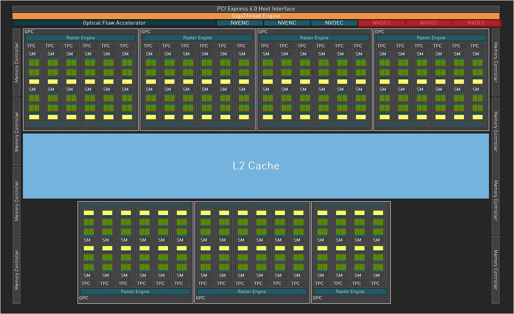
The GeForce RTX 4080 Super is based on the same 5 nm AD103 silicon as the original RTX 4080. As a SKU, it has a lot in common with the RTX 2080 Super, which had maxed out the TU104 silicon, while the original RTX 2080 wasn't too far behind. The AD103 is NVIDIA's second largest silicon, powering not just the RTX 4080 and the RTX 4080 Super, but also the mobile RTX 4090. This 379 mm² beast packs nearly 46 billion transistors—more than that of the previous generation flagship GA102. It has 80 streaming multiprocessors, and since the RTX 4080 Super maxes the chip out, all 80 are enabled. This gives the RTX 4080 Super a phenomenal CUDA core count of 10,240, with 320 Tensor cores, 80 RT cores, 320 TMUs, and all of the chip's 112 ROPs. The AD103 features a 256-bit wide memory interface, and the RTX 4080 Super continues to get 16 GB of memory, running at 23 Gbps—higher than the 22.4 Gbps of the RTX 4080.
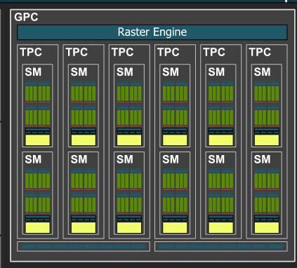
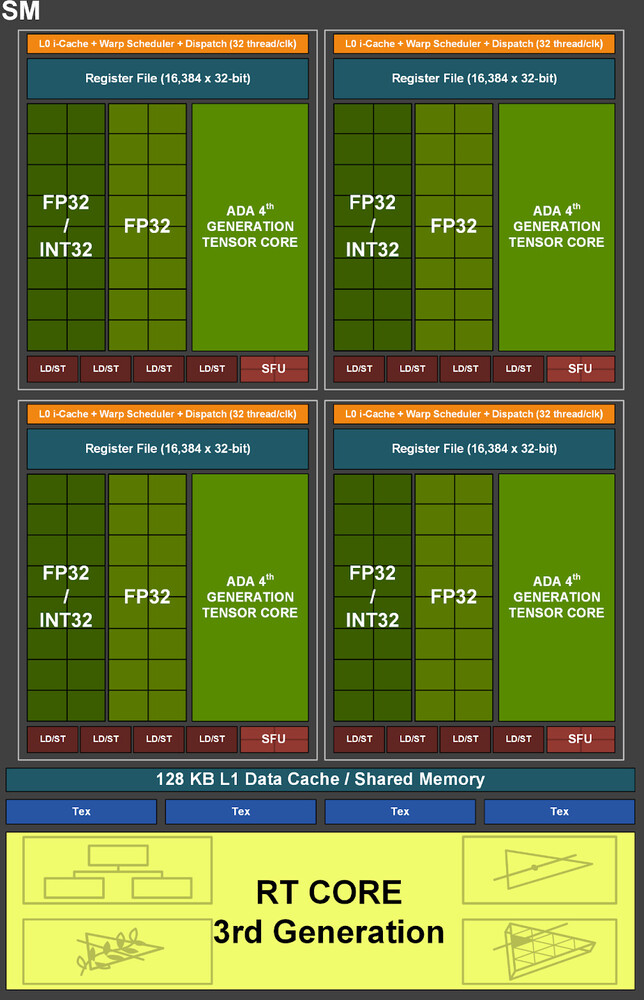
The AD103 features a PCI-Express 4.0 x16 host interface along with support for PCI resizable BAR; and its 256-bit wide GDDR6X memory interface. The GigaThread Engine serves as the main workflow controller for the GPU, dispatching work among the GPU's 7 graphics processing clusters (GPCs). Each GPC shares a Raster Engine and render backends among six texture processing clusters (TPCs), the indivisible subunit of the GPU; one of the GPCs has just four TPCs. Each TPC has two Streaming Multiprocessors (SM), and a Polymorph unit. Each SM contains 128 CUDA cores across four partitions. Half of these CUDA cores are pure-FP32; while the other half is capable of FP32 or INT32. The SM retains concurrent FP32+INT32 math processing capability. The SM also contains a 3rd generation RT core, four 4th generation Tensor cores, some cache memory, and four TMUs. One of the seven GPCs on the AD103 physically only has four TPCs.
With 80 SM that have 128 CUDA cores, each; we arrive at 10,240 CUDA cores. NVIDIA says that the RTX 4080 Super maxes out the AD103 silicon; and this statement is 99.999% true. The AD103 has four NVDEC and two NVENC units on the silicon; but for the RTX 4080 Super, just like the RTX 4080, three of these NVDEC units are disabled. This is irrelevant for a GeForce RTX product, and NVIDIA only put those large numbers of NVDEC units for pro-visualization graphics cards, such as the RTX 5000 Ada.
3rd Gen RT Core and Ray Tracing

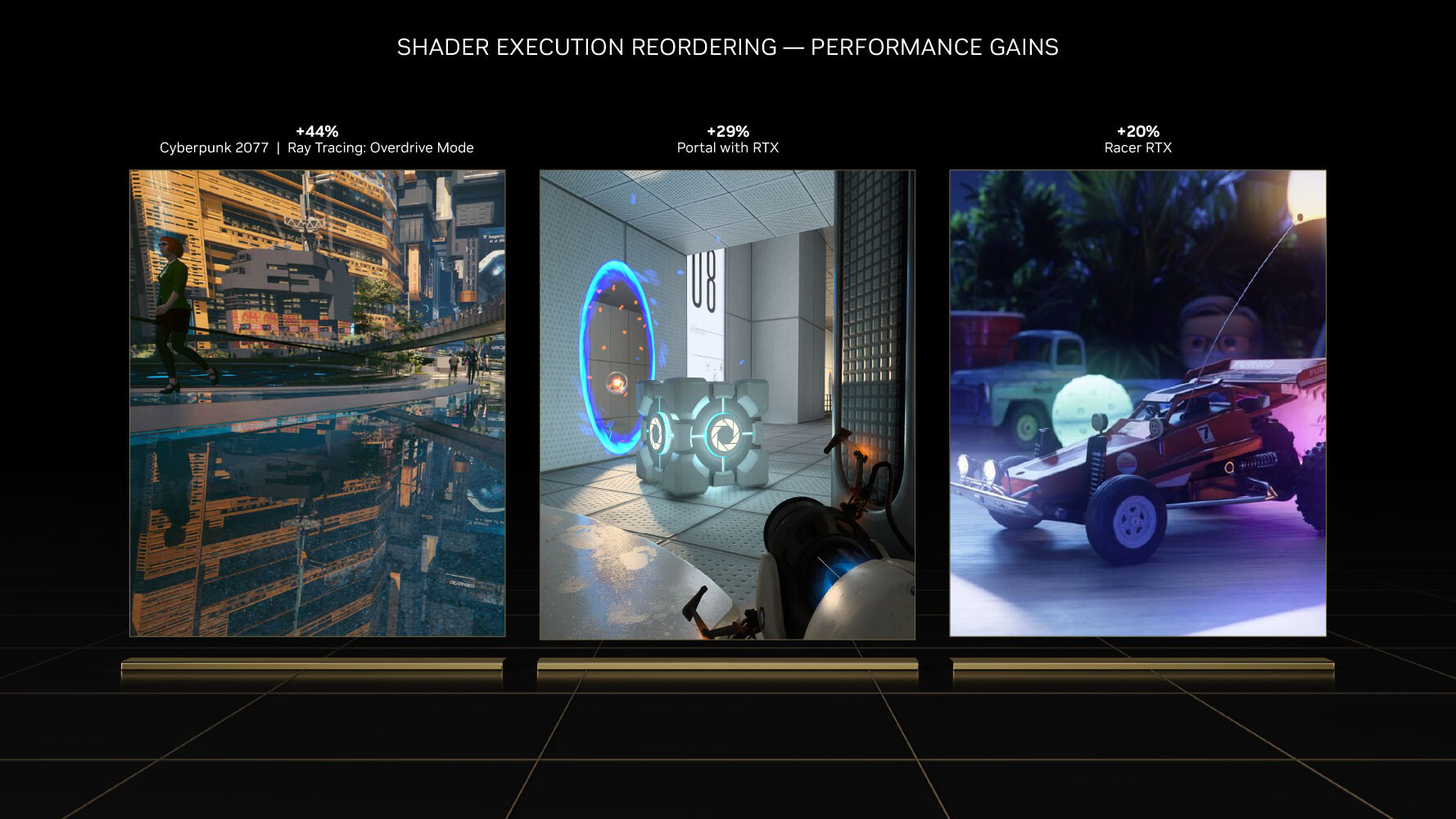
The 3rd generation RT core accelerates the most math-intensive aspects of real-time ray tracing, including BVH traversal. Displaced micro-mesh engine is a revolutionary feature introduced with the new 3rd generation RT core. Just as mesh shaders and tessellation have had a profound impact on improving performance with complex raster geometry, allowing game developers to significantly increase geometric complexity; DMMs is a method to reduce the complexity of the bounding-volume hierarchy (BVH) data-structure, which is used to determine where a ray hits geometry. Previously, the BVH had to capture even the smallest details to properly determine the intersection point. Ada's ray tracing architecture also receives a major performance uplift from Shader Execution Reordering (SER), a software-defined feature that requires awareness from game-engines, to help the GPU reorganize and optimize worker threads associated with ray tracing.


The BVH now needn't have data for every single triangle on an object, but can represent objects with complex geometry as a coarse mesh of base triangles, which greatly simplifies the BVH data structure. A simpler BVH means less memory consumed and helps to greatly reduce ray tracing CPU load, because the CPU only has to generate a smaller structure. With older "Ampere" and "Turing" RT cores, each triangle on an object had to be sampled at high overhead, so the RT core could precisely calculate ray intersection for each triangle. With Ada, the simpler BVH, plus the displacement maps can be sent to the RT core, which is now able to figure out the exact hit point on its own. NVIDIA has seen 11:1 to 28:1 compression in total triangle counts. This reduces BVH compile times by 7.6x to over 15x, in comparison to the older RT core; and reducing its storage footprint by anywhere between 6.5 to 20 times. DMMs could reduce disk- and memory bandwidth utilization, utilization of the PCIe bus, as well as reduce CPU utilization. NVIDIA worked with Simplygon and Adobe to add DMM support for their tool chains.
Opacity Micro Meshes


Opacity Micro Meshes (OMM) is a new feature introduced with Ada to improve rasterization performance, particularly with objects that have alpha (transparency data). Most low-priority objects in a 3D scene, such as leaves on a tree, are essentially rectangles with textures on the leaves where the transparency (alpha) creates the shape of the leaf. RT cores have a hard time intersecting rays with such objects, because they're not really in the shape that they appear (they're really just rectangles with textures that give you the illusion of shape). Previous-generation RT cores had to have multiple interactions with the rendering stage to figure out the shape of a transparent object, because they couldn't test for alpha by themselves.


This has been solved by using OMMs. Just as DMMs simplify geometry by creating meshes of micro-triangles; OMMs create meshes of rectangular textures that align with parts of the texture that aren't alpha, so the RT core has a better understanding of the geometry of the object, and can correctly calculate ray intersections. This has a significant performance impact on shading performance in non-RT applications, too. Practical applications of OMMs aren't just low-priority objects such as vegetation, but also smoke-sprites and localized fog. Traditionally there was a lot of overdraw for such effects, because they layered multiple textures on top of each other, that all had to be fully processed by the shaders. Now only the non-opaque pixels get executed—OMMs provide a 30 percent speedup with graphics buffer fill-rates, and a 10 percent impact on frame-rates.
DLSS 3 Frame Generation
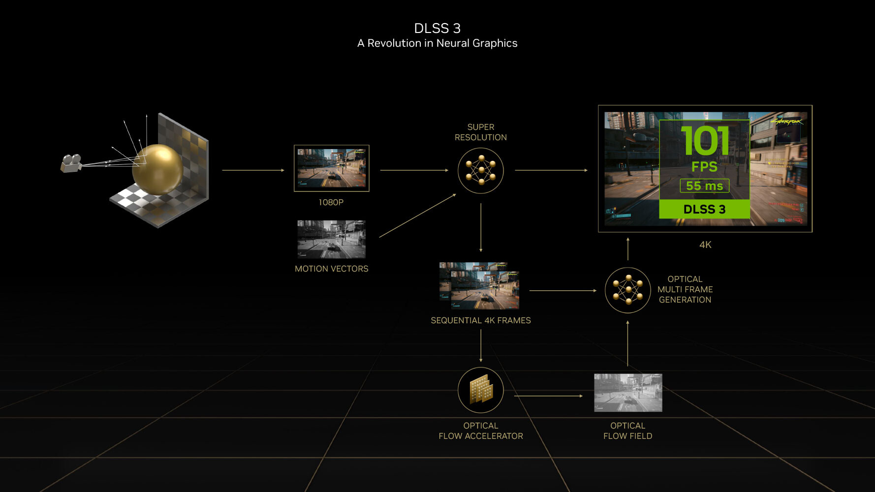

DLSS 3 introduces a revolutionary new feature that promises a doubling in frame-rate at comparable quality, it's called AI frame-generation. Building on DLSS 2 and its AI super-resolution (scaling up a lower-resolution frame to native resolution with minimal quality loss); DLSS 3 can generate entire frames simply using AI, without involving the graphics rendering pipeline, it's also possible to enable frame generation at native resolution without upscaling. Later in the article, we will show you DLSS 3 in action.

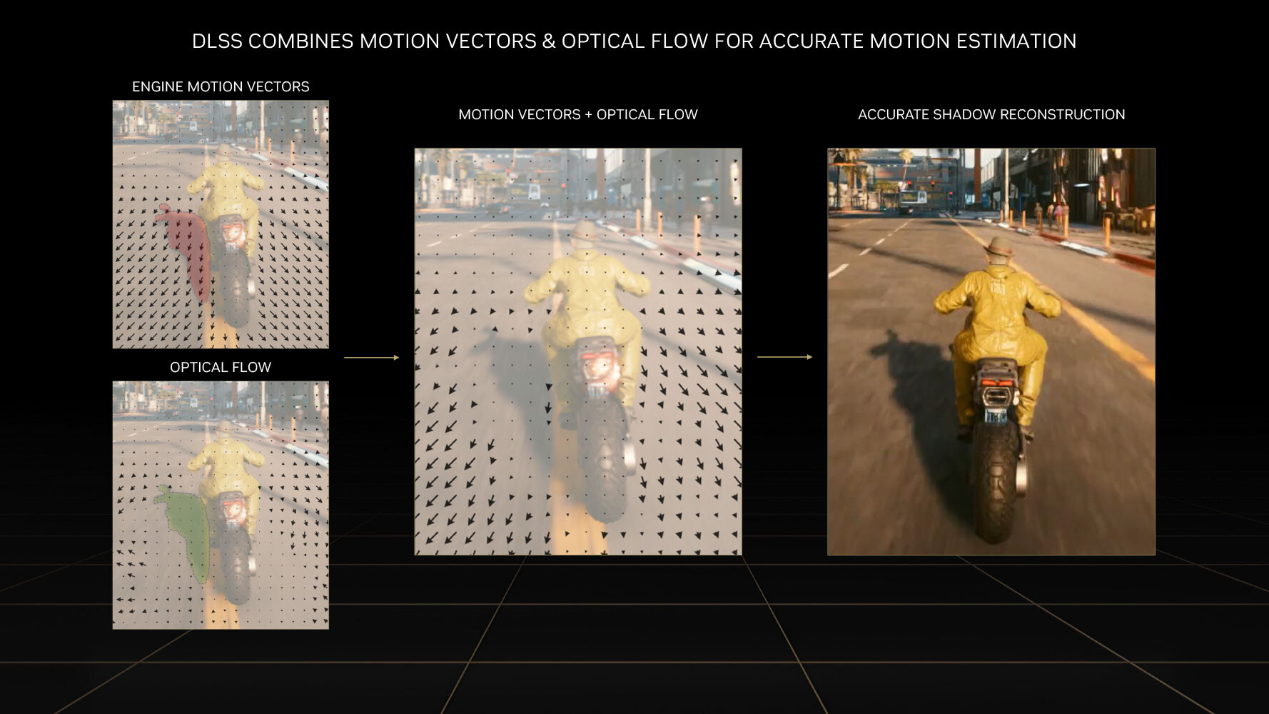
Every alternating frame with DLSS 3 is hence AI-generated, without being a replica of the previous rendered frame. This is possible only on the Ada graphics architecture, because of a hardware component called the optical flow accelerator (OFA), which assists in predicting what the next frame could look like, by creating what NVIDIA calls an optical flow-field. OFA ensures that the DLSS 3 algorithm isn't confused by static objects in a rapidly-changing 3D scene (such as a race sim). The process heavily relies on the performance uplift introduced by the FP8 math format of the 4th generation Tensor core. A third key ingredient of DLSS 3 is Reflex. By reducing the rendering queue to zero, Reflex plays a vital role in ensuring that latency with DLSS 3 enabled is at an acceptable level. A combination of OFA and the 4th Gen Tensor core is why the Ada architecture is required to use DLSS 3, and why it won't work on older architectures.
Packaging

The Card
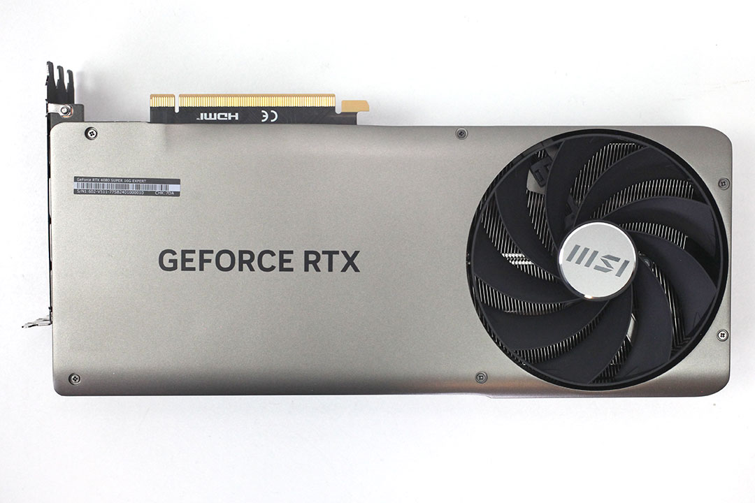

With the Expert line, MSI is introducing a new design theme for their lineup and I have to say it looks mighty good. Both the main cooler shroud and the backplate are made from high-quality metal with a nice matte surface texture. The card is designed so that hot air gets exhausted out of the case by the front fan and the back fan pulls air through the card.
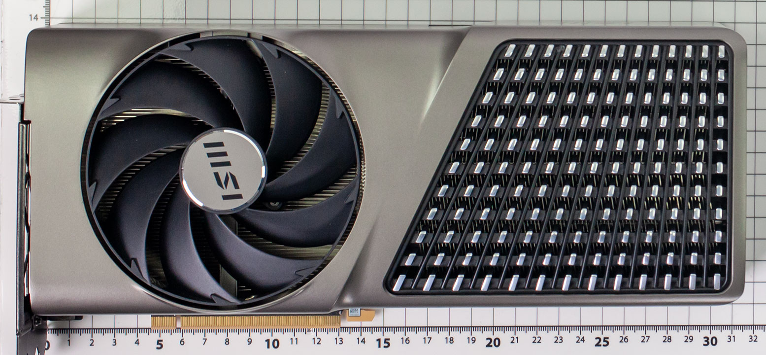
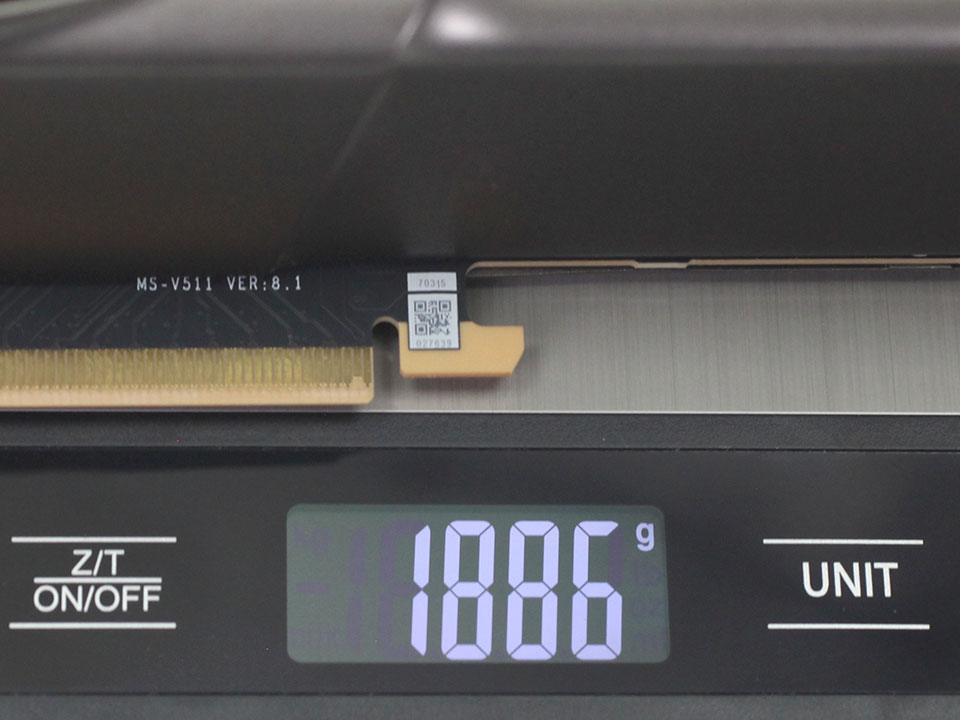
Dimensions of the card are 31.0 x 14.0 cm, and it weighs 1886 g.
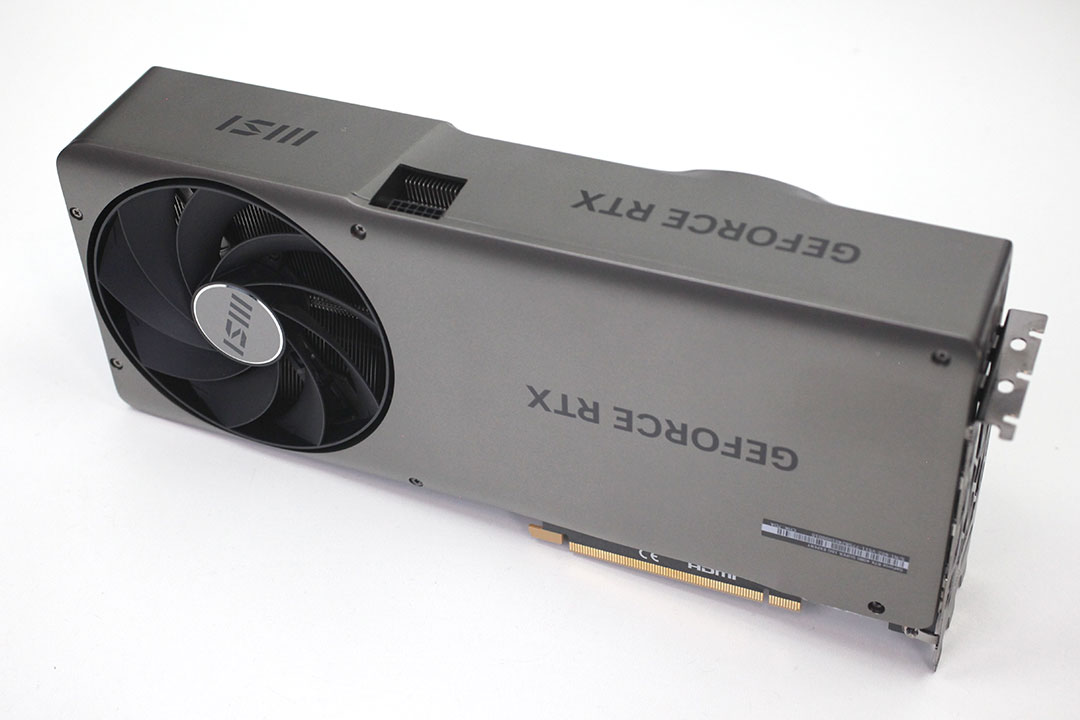
Installation requires three slots in your system. We measured the card's width to be 61 mm.
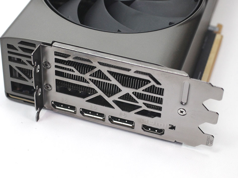
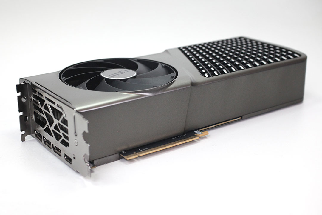
Display connectivity includes three standard DisplayPort 1.4a ports and one HDMI 2.1a (same as Ampere and same as non-Super Ada).
NVIDIA introduced the concept of dual NVDEC and NVENC Codecs with the Ada Lovelace architecture. This means there are two independent sets of hardware-accelerators; so you can encode and decode two streams of video in parallel or one stream at double the FPS rate. The new 8th Gen NVENC now accelerates AV1 encoding, besides HEVC. You also get an "optical flow accelerator" unit that is able to calculate intermediate frames for videos, to smooth playback. The same hardware unit is used for frame generation in DLSS 3.
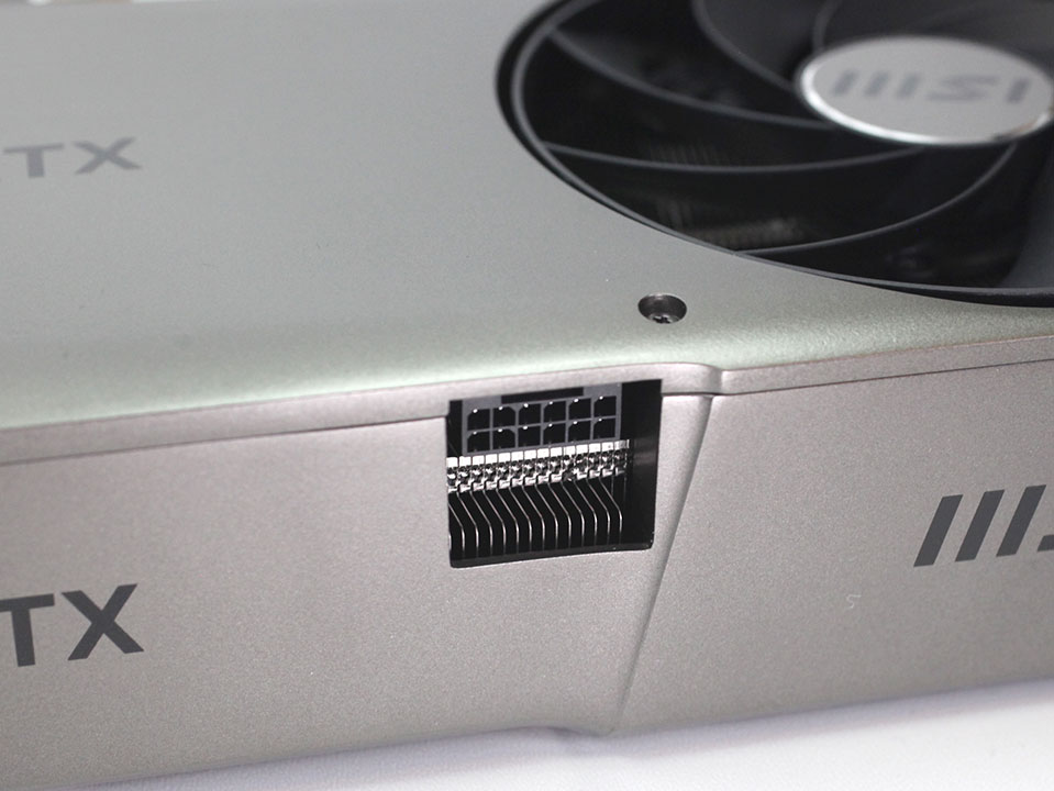
All GeForce RTX 4080 and 4080 Super graphics cards use the 12+4 pin ATX 12VHPWR connector, an adapter cable is included in the box.
Our Patreon Silver Supporters can read articles in single-page format.
Mar 13th, 2025 06:59 EDT
change timezone
Latest GPU Drivers
New Forum Posts
- The TPU UK Clubhouse (25882)
- What's your latest tech purchase? (23291)
- Free Games Thread (4553)
- 3D Printer Club (451)
- How's your old spinner holding up? (48)
- I'm looking for a good tool to make the 3D scanning of my mini-pc using the photogrammetry and my Kinect 2. (87)
- Missing nvidia control panel after using nvcleanstall with latest drivers (4)
- Zen6 is almost here ? (67)
- Core i7 12700k or Ryzen 7 7700? (13)
- Post your Old CDs & FDs, from back in the day thread. (72)
Popular Reviews
- AMD Ryzen 9 9950X3D Review - Great for Gaming and Productivity
- Sapphire Radeon RX 9070 XT Nitro+ Review - Beating NVIDIA
- XFX Radeon RX 9070 XT Mercury OC Magnetic Air Review
- Dough Spectrum Black 32 Review
- FSP MP7 Black Review
- ASUS Radeon RX 9070 TUF OC Review
- ASUS GeForce RTX 5090 TUF Review
- AMD Ryzen 7 9800X3D Review - The Best Gaming Processor
- NVIDIA GeForce RTX 5070 Founders Edition Review
- MSI MAG B850 Tomahawk Max Wi-Fi Review
Controversial News Posts
- NVIDIA GeForce RTX 50 Cards Spotted with Missing ROPs, NVIDIA Confirms the Issue, Multiple Vendors Affected (513)
- AMD Radeon RX 9070 and 9070 XT Listed On Amazon - One Buyer Snags a Unit (261)
- AMD RDNA 4 and Radeon RX 9070 Series Unveiled: $549 & $599 (260)
- AMD Mentions Sub-$700 Pricing for Radeon RX 9070 GPU Series, Looks Like NV Minus $50 Again (249)
- NVIDIA Investigates GeForce RTX 50 Series "Blackwell" Black Screen and BSOD Issues (244)
- AMD Radeon RX 9070 and 9070 XT Official Performance Metrics Leaked, +42% 4K Performance Over Radeon RX 7900 GRE (195)
- AMD Radeon RX 9070-series Pricing Leaks Courtesy of MicroCenter (158)
- AMD Radeon RX 9070 XT Reportedly Outperforms RTX 5080 Through Undervolting (102)