 74
74
MSI GeForce RTX 5090 Suprim SOC Review
(74 Comments) »Introduction
MSI GeForce RTX 5090 SUPRIM SOC is the company's most premium air-cooled custom design graphics card based on the new RTX 5090 Blackwell, the flagship RTX 50-series GPU, designed to not just max all current and upcoming games at 4K Ultra HD, but also unlock new experiences never before imagined, such as 8K 60 Hz or even 120 Hz. Today we are also reviewing this card's liquid-cooled sister, the MSI RTX 5090 SUPRIM Liquid SOC, so be sure to check out that review too, to see which cooling option is more practical for you. The SUPRIM line of graphics cards are a rather recent addition to MSI's graphics card product stack, introduced with the RTX 30-series. These cards represent the pinnacle of MSI's product design. The company is looking to meet or exceed the form and function combination standards set by NVIDIA's first-party Founders Edition graphics cards, while also having superior cooling performance, noise, and a much higher factory overclock to boot. There are actually two variants of the air-cooled RTX 5090 SUPRIM, the OC and SOC (super overclock), both of which are clocked higher than MSI's other custom RTX 5090 models. We are reviewing the SOC today.

The GeForce RTX 5090 heralds NVIDIA's new GeForce Blackwell graphics architecture, and with it, a major industry standard addition to the way real time graphics is rendered, called Neural Rendering. You've probably already been blown away by generative AI, and its ability to conjure up photorealistic images and video. NVIDIA and its allied researchers have invented a way to bring generative AI models closer to the graphics rendering pipeline, making the AI create portions of a 3D scene. This is enabled by a new API-level access to the Tensor cores of the GPU, and the introduction of a new on-chip AI acceleration resource management component called AMP. This is different from DLSS, where AI is used to reconstruct details in an upscaled frame. Blackwell also introduces DLSS 4, which introduces new transformer-based AI models to all the subcomponents (super resolution, frame generation, etc.), and introduces Multi Frame Generation, the ability for an AI model to create not just every other frame, but up to three succeeding frames to a traditionally rendered frame, without any of the blur, latency, or other optical artifacts expected of such a technique. Multi Frame Generation makes it possible to play today's games at 8K with 60 Hz, if you have such a TV or a display, or even high refresh-rate gameplay at 4K.
Perhaps the most striking aspect of Blackwell is that unlike every new graphics architecture from NVIDIA in the past decade, it does not introduce a new foundry node. That's right, the RTX 5090 is built on the same NVIDIA co-engineered variant of the 5 nm EUV from TSMC, called simply TSMC 4N—the exact same node on which the RTX 40-series Ada generation of GPUs is built on. And yet, the company promises generational gains in performance-per-Watt. This is thanks entirely to the performance of the new architecture, paired with a completely re-architected power management solution that we'll talk about in the next page.
The RTX 5090 is a no-holds-barred flagship product, and is based on the largest GPU from the family, codenamed GB202. This is the first gaming GPU to introduce a PCI-Express 5.0 x16 host interface, and the new GDDR7 memory standard that doubles speeds over the GDDR6. The RTX 5090 comes with a mammoth 21,760 CUDA cores, 680 Tensor cores, and 170 RT cores, across 11 GPCs, and this doesn't even max out the GB202. The card comes with 32 GB of 28 Gbps GDDR7 memory across a 512-bit wide memory bus, giving it 1.79 TB/s of memory bandwidth. The GPU needs this kind of memory bandwidth to pull off neural rendering, and you'll find massive increases in memory bandwidth to be a common trend across all upcoming RTX 50-series GPUs, thanks to GDDR7.
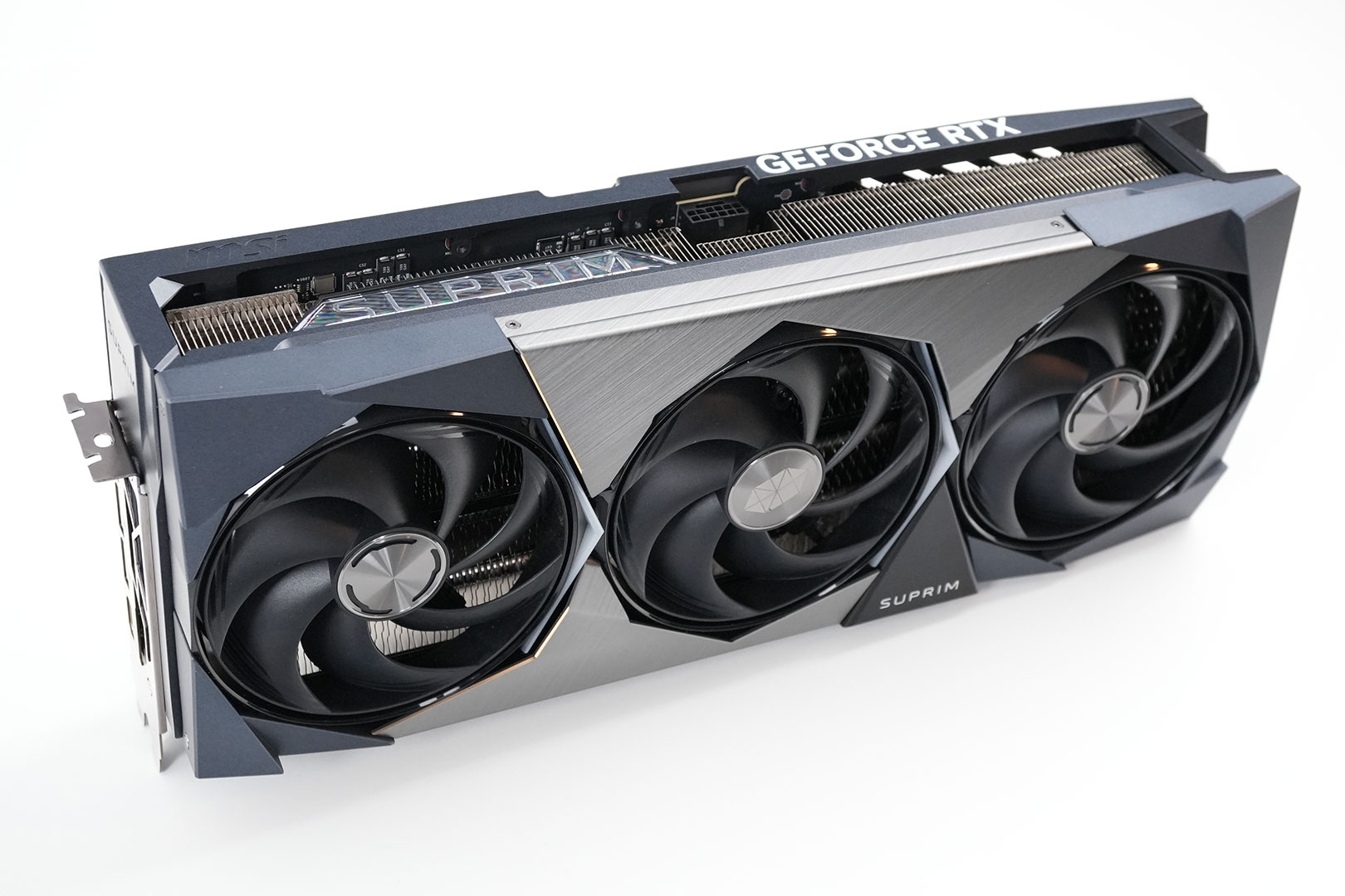
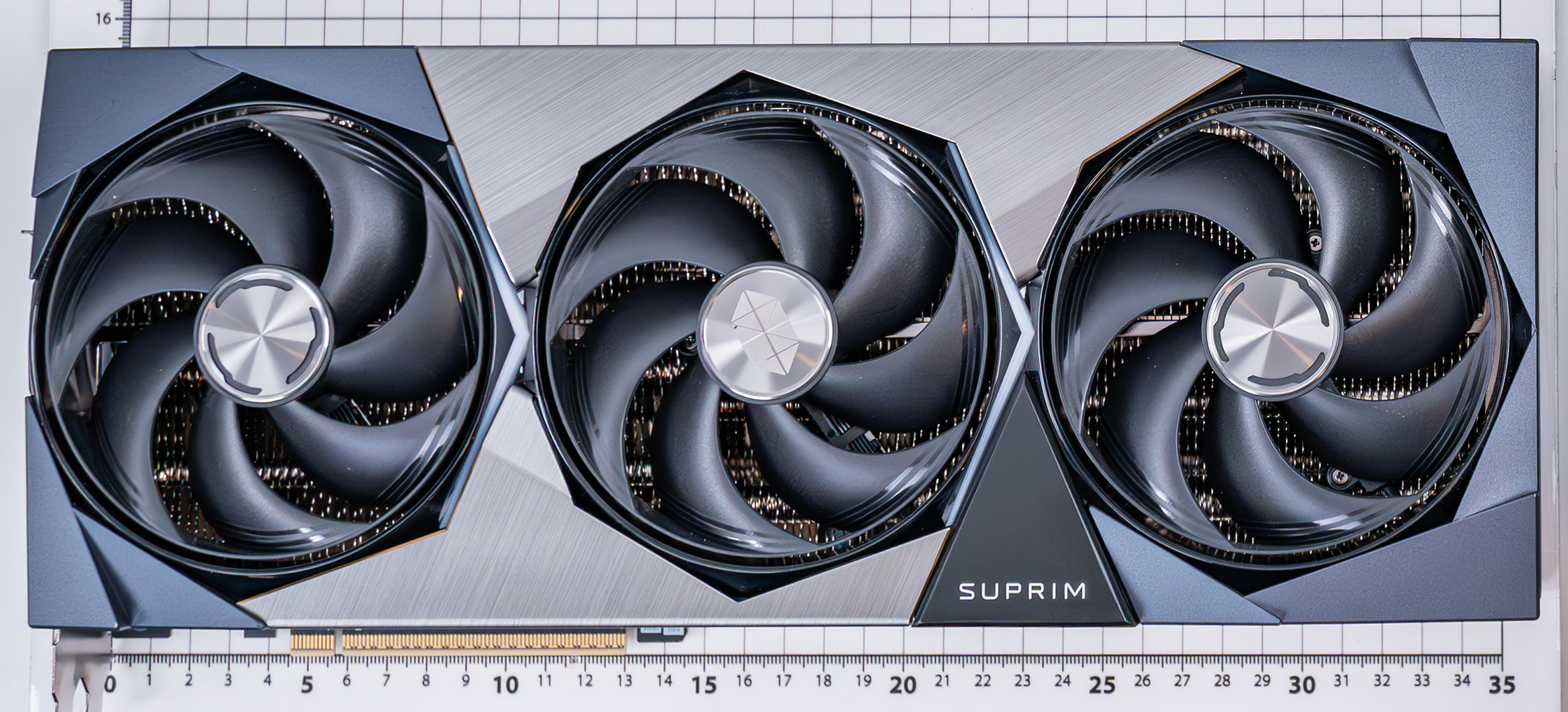
The MSI RTX 5090 SUPRIM SOC is designed to resemble jewellery, its cooling solution is made of the most premium materials, machined to perfection. The card debuts MSI's new Hyper Frozr SUPRIM cooling solution, featuring a sturdy outer frame that suspends the rest of the card. A large vapor chamber baseplate pulls heat from the GB202 ASIC, and the sixteen GDDR7 memory chips, conveying it to an arrangement of seven heat pipes that are flattened and bunched up over this vapor chamber. The heatsink is ventilated by three of MSI's latest StormForce axial airflow fans, which aren't just webbed toward the edges, but also feature serrations. There is a tastefully executed ARGB LED lighting setup, and the highlight of MSI's original design has to be its 3D backplate, which gives the card an industrial look when installed. Lastly, the card comes with MSI's highest factory overclock for the RTX 5090, with the GPU boosting up to 2565 MHz (vs. 2407 MHz reference). This may not seem like much, but the whole point of this nearly 4-pound cooling solution is to ensure the GPU holds onto boost frequencies better, by keeping temperatures lower. Out of the box, though, both our MSI SUPRIM samples came with the BIOS switch in the "silent" setting, which boosts up to 2512 MHz. We test cards in the BIOS setting they come with, out of the box. MSI is asking $2,400 for this card, which is a stiff 20% premium over the baseline price.
| Price | Cores | ROPs | Core Clock | Boost Clock | Memory Clock | GPU | Transistors | Memory | |
|---|---|---|---|---|---|---|---|---|---|
| RTX 3080 | $420 | 8704 | 96 | 1440 MHz | 1710 MHz | 1188 MHz | GA102 | 28000M | 10 GB, GDDR6X, 320-bit |
| RTX 4070 | $490 | 5888 | 64 | 1920 MHz | 2475 MHz | 1313 MHz | AD104 | 35800M | 12 GB, GDDR6X, 192-bit |
| RX 7800 XT | $440 | 3840 | 96 | 2124 MHz | 2430 MHz | 2425 MHz | Navi 32 | 28100M | 16 GB, GDDR6, 256-bit |
| RX 6900 XT | $450 | 5120 | 128 | 2015 MHz | 2250 MHz | 2000 MHz | Navi 21 | 26800M | 16 GB, GDDR6, 256-bit |
| RX 6950 XT | $630 | 5120 | 128 | 2100 MHz | 2310 MHz | 2250 MHz | Navi 21 | 26800M | 16 GB, GDDR6, 256-bit |
| RTX 3090 | $900 | 10496 | 112 | 1395 MHz | 1695 MHz | 1219 MHz | GA102 | 28000M | 24 GB, GDDR6X, 384-bit |
| RTX 4070 Super | $590 | 7168 | 80 | 1980 MHz | 2475 MHz | 1313 MHz | AD104 | 35800M | 12 GB, GDDR6X, 192-bit |
| RX 7900 GRE | $530 | 5120 | 160 | 1880 MHz | 2245 MHz | 2250 MHz | Navi 31 | 57700M | 16 GB, GDDR6, 256-bit |
| RTX 4070 Ti | $700 | 7680 | 80 | 2310 MHz | 2610 MHz | 1313 MHz | AD104 | 35800M | 12 GB, GDDR6X, 192-bit |
| RTX 4070 Ti Super | $750 | 8448 | 96 | 2340 MHz | 2610 MHz | 1313 MHz | AD103 | 45900M | 16 GB, GDDR6X, 256-bit |
| RX 7900 XT | $620 | 5376 | 192 | 2000 MHz | 2400 MHz | 2500 MHz | Navi 31 | 57700M | 20 GB, GDDR6, 320-bit |
| RTX 3090 Ti | $1000 | 10752 | 112 | 1560 MHz | 1950 MHz | 1313 MHz | GA102 | 28000M | 24 GB, GDDR6X, 384-bit |
| RTX 4080 | $940 | 9728 | 112 | 2205 MHz | 2505 MHz | 1400 MHz | AD103 | 45900M | 16 GB, GDDR6X, 256-bit |
| RTX 4080 Super | $990 | 10240 | 112 | 2295 MHz | 2550 MHz | 1438 MHz | AD103 | 45900M | 16 GB, GDDR6X, 256-bit |
| RX 7900 XTX | $820 | 6144 | 192 | 2300 MHz | 2500 MHz | 2500 MHz | Navi 31 | 57700M | 24 GB, GDDR6, 384-bit |
| RTX 4090 | $2400 | 16384 | 176 | 2235 MHz | 2520 MHz | 1313 MHz | AD102 | 76300M | 24 GB, GDDR6X, 384-bit |
| RTX 5090 | $2000 | 21760 | 176 | 2017 MHz | 2407 MHz | 1750 MHz | GB202 | 92200M | 32 GB, GDDR7, 512-bit |
| MSI RTX 5090 Suprim SOC | $2400 | 21760 | 176 | 2017 MHz | 2512 MHz | 1750 MHz | GB202 | 92200M | 32 GB, GDDR7, 512-bit |
NVIDIA Blackwell Architecture
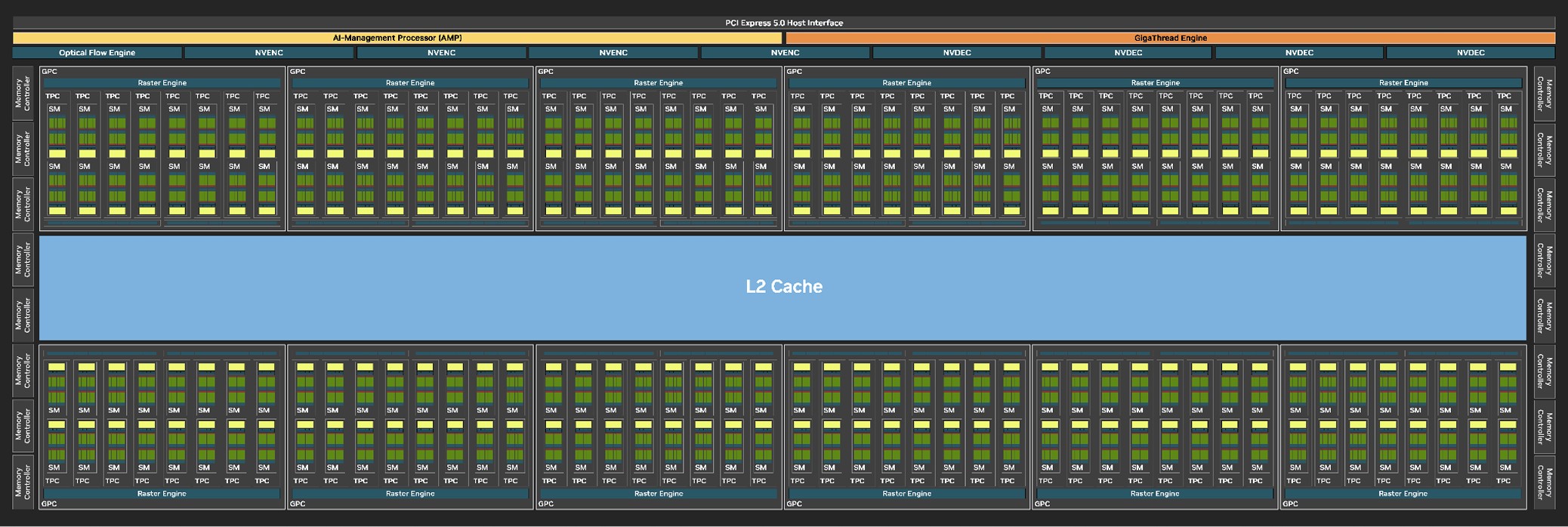
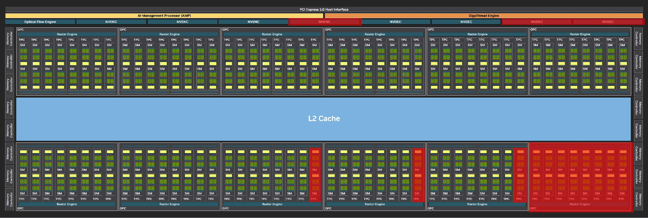
The GeForce Blackwell graphics architecture heralds NVIDIA's 4th generation of RTX, the late-2010s re-invention of the modern GPU that sees a fusion of real time ray traced objects with conventional raster 3D graphics. With Blackwell, NVIDIA is helping add another dimension, neural rendering, the ability for the GPU to leverage a generative AI to create portions of a frame. This is different from DLSS, where an AI model is used to reconstruct details in an upscaled frame based on its training date, temporal frames, and motion vectors. At the heart of the GeForce RTX 5090 we are reviewing today is the mammoth 5 nm GB202 silicon. This is one of the largest monolithic dies ever designed by NVIDIA, measuring 750 mm², compared to the 608.5 mm² of the AD102 die. The process is unchanged between the two generations—it's still an NVIDIA-specific variant of TSMC 5 nm EUV, dubbed TSMC 4N. The GB202 rocks 92.2 billion transistors, a 20% increase over the AD102.
The GB202 silicon is laid out essentially in the same component hierarchy as past generations of NVIDIA GPUs, but with a few notable changes. The GPU features PCI-Express 5.0 x16, making it the first gaming GPU to do so. PCIe Gen 5 has been around since Intel's 12th Gen Core "Alder Lake" and AMD's Ryzen 7000 "Zen 4," so there is a sizable install-base of systems that can take advantage of it. The GPU is of course compatible with older generations of PCIe. Whether this affects performance is a question we cover in our separate RTX 5090 PCIe Scaling Article. The GB202 is also the first GPU to implement the new GDDR7 memory standard, which doubles speeds over GDDR6 while lowering the energy cost of bandwidth. NVIDIA left no half-measures with the GB202, and gave it a broad 512-bit GDDR7 memory interface. On the RTX 5090, this is configured with 32 GB of 28 Gbps GDDR7. Upcoming RTX 50-series SKUs could have narrower memory interfaces but with higher memory speeds, and some professional graphics cards based on the GB202 could even use high-density memory chips.
The GigaThread Engine is the main graphics rendering workload allocation logic on the GB202, but there's a new addition, a dedicated serial processor for managing all AI acceleration resources on the GPU, NVIDIA calls this AMP (AI management processor). Other components at the global level are the Optical Flow Processor, a component involved in older versions of DLSS frame generation and for video encoding; and a vast media acceleration engine consisting of four NVENC encode accelerators, and four NVDEC decode accelerators. The new 9th Gen NVENC video encode accelerators come with 4:2:2 AV1 and HEVC encoding support. The RTX 5090 has 3 out of 4 NVENC and 2 out of 4 NVDEC units enabled. The central region of the GPU has the single largest common component, the 128 MB L2 cache. The RTX 5090 is configured with 96 MB of it.
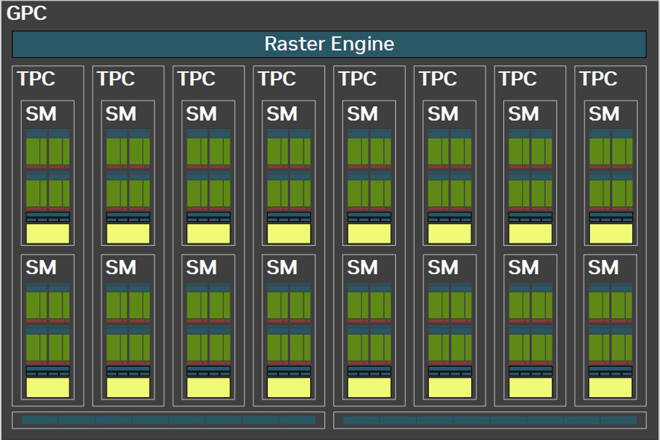
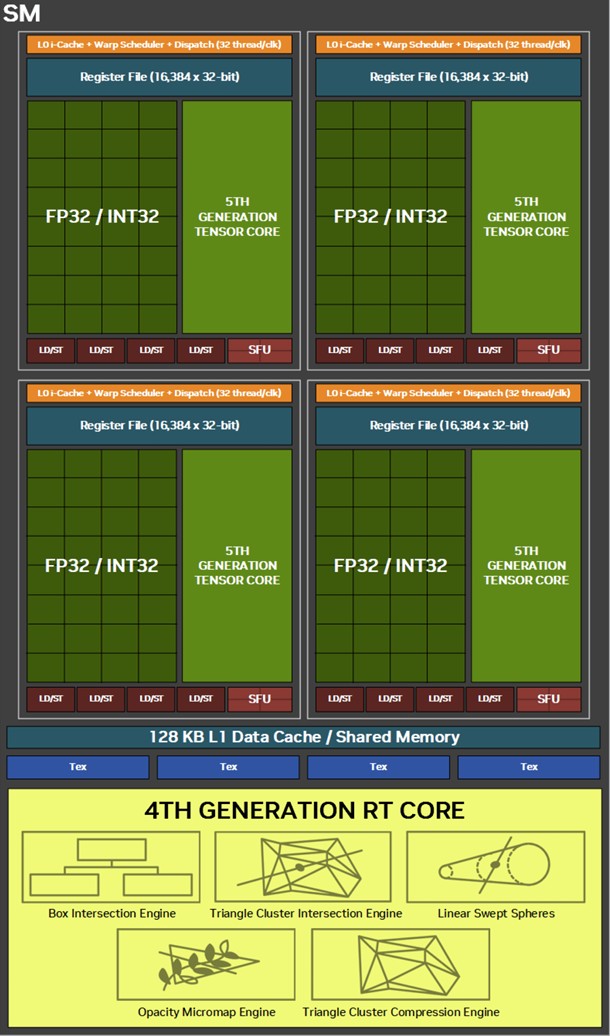

Each graphics processing cluster (GPC) is a subdivision of the GPU with nearly all components needed for graphics rendering. On the GB202, a GPC consists of 16 streaming multiprocessors (SM) across 8 texture processing clusters (TPCs), and a raster engine consisting of 16 ROPs. Each SM contains 128 CUDA cores. Unlike the Ada generation SM that each had 64 FP32+INT32 and 64 purely-FP32 SIMD units, the new Blackwell generation SM features concurrent FP32+INT32 capability on all 128 SIMD units. These 128 CUDA cores are arranged in four slices, each with a register file, a level-0 instruction cache, a warp scheduler, two sets of load-store units, and a special function unit (SFU) handling some special math functions such as trigonometry, exponents, logarithms, reciprocals, and square-root. The four slices share a 128 KB L1 data cache, and four TMUs. The most exotic components of the Blackwell SM are the four 5th Gen Tensor cores, and a 4th Gen RT core.
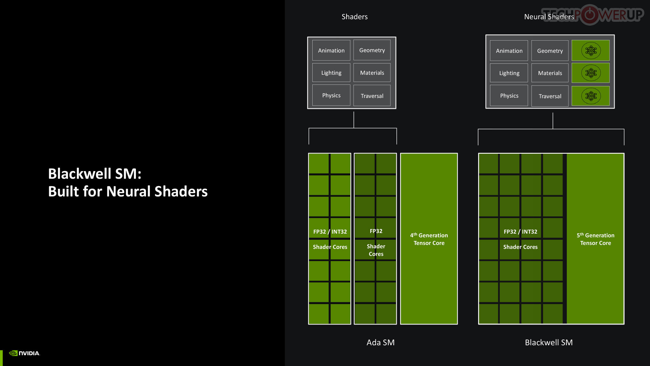
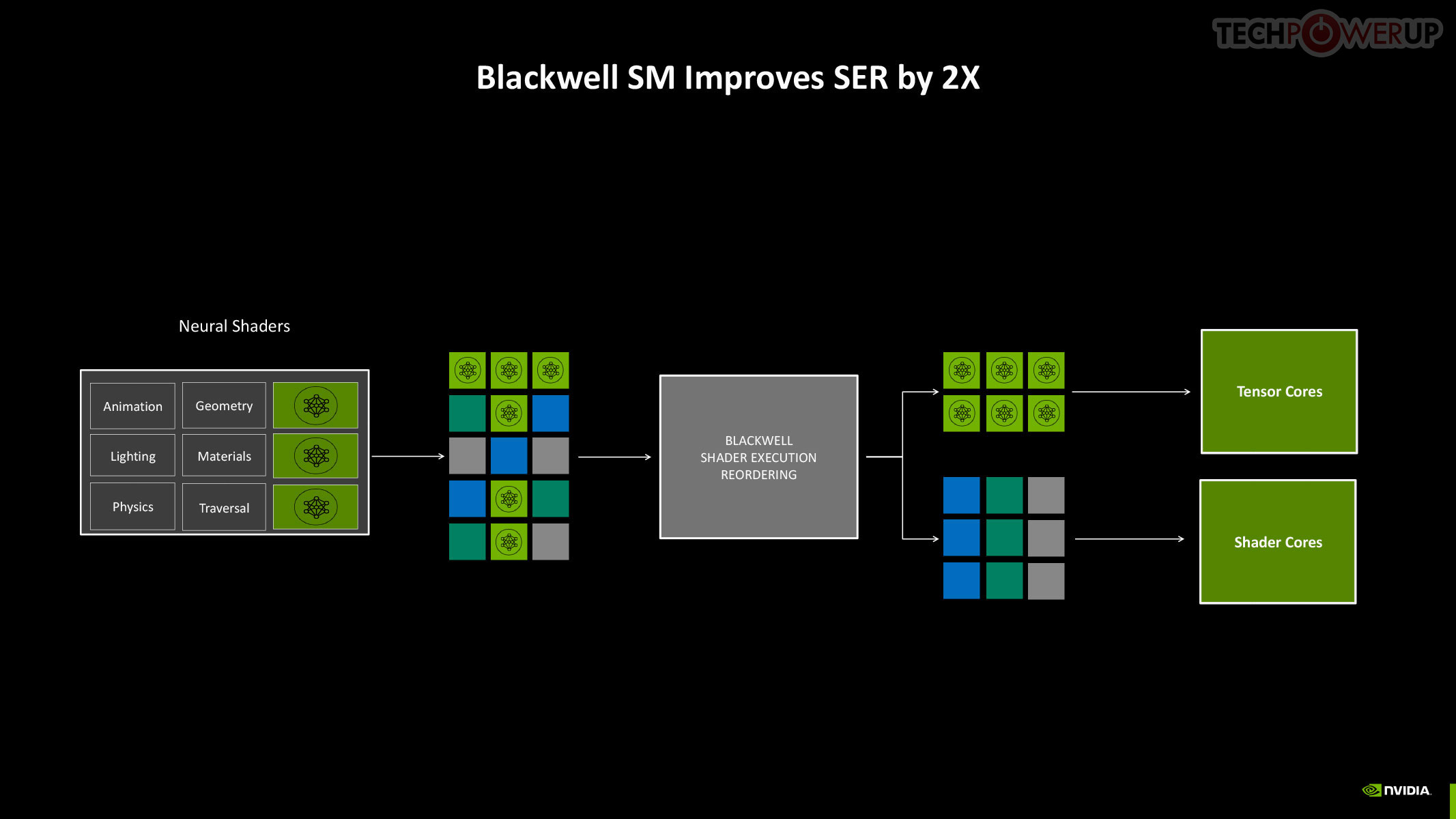
Perhaps the biggest change to the way the SM handles work introduced with Blackwell is the concept of neural shaders—treating portions of the graphics rendering workload done by a generative AI model as shaders. Microsoft has laid the groundwork for standardization of neural shaders with its Cooperative Vectors API, in the latest update to DirectX 12. The Tensor cores are now accessible for workloads through neural shaders, and the shader execution reordering (SER) engine of the Blackwell SM is able to more accurately reorder workloads for the CUDA cores and the Tensor core in an SM.
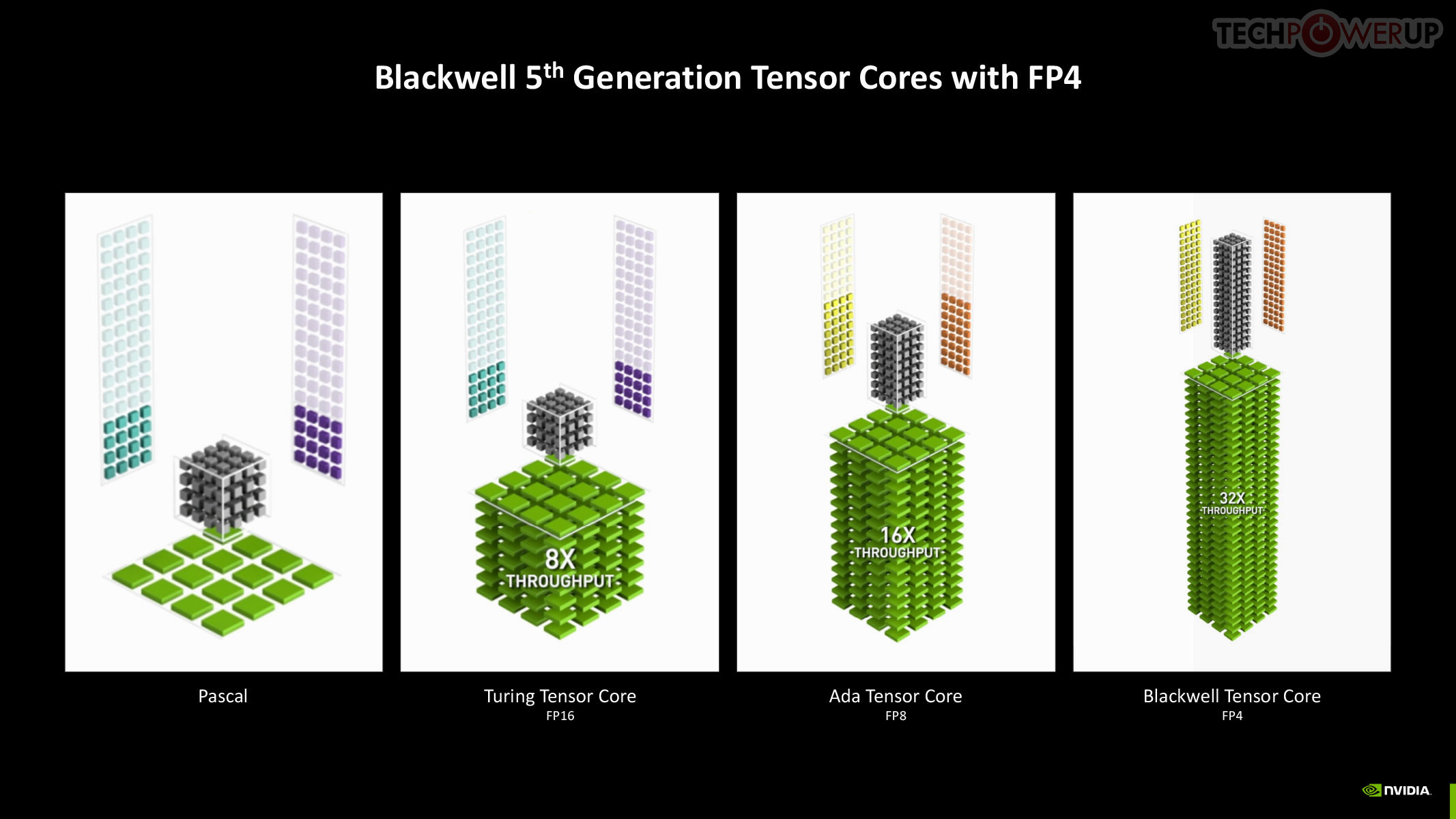

The new 5th Gen Tensor core introduces support for FP4 data format (1/8 precision) to fast moving atomic workloads, providing 32 times the throughput of the very first Tensor core introduced with the Volta architecture. Over the generations, AI models leveraged lesser precision data formats, and sparsity, to improve performance. The AI management processor (AMP) is what enables simultaneous AI and graphics workloads at the highest levels of the GPU, so it could be simultaneously rendering real time graphics for a game, while running an LLM, without either affecting the performance of the other. AMP is a specialized hardware scheduler for all the AI acceleration resources on the silicon. This plays a crucial role for DLSS 4 multi-frame generation to work.
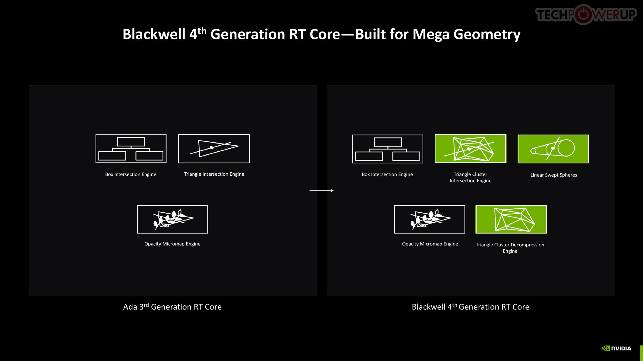
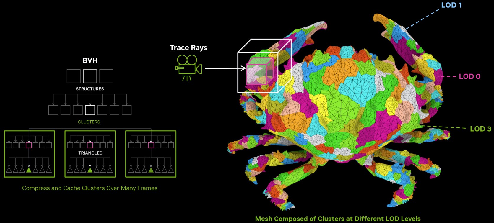
The 4th Gen RT core not just offers a generational increase in ray testing and ray intersection performance, which lowers the performance cost of enabling path tracing and ray traced effects; but also offers a potential generational leap in performance with the introduction of Mega Geometry. This allows for ray traced objects with extremely high polygon counts, increasing their detail. Poly count and ray tracing present linear increases in performance costs, as each triangle has to intersect with a ray, and there should be sufficient rays to intersect with each of them. This is achieved by adopting clusters of triangles in an object as first-class primitives, and cluster-level acceleration structures. The new RT cores introduce a component called a triangle cluster intersection engine, designed specifically for handling mega geometry. The integration of a triangle cluster compression format and a lossless decompression engine allows for more efficient processing of complex geometry.
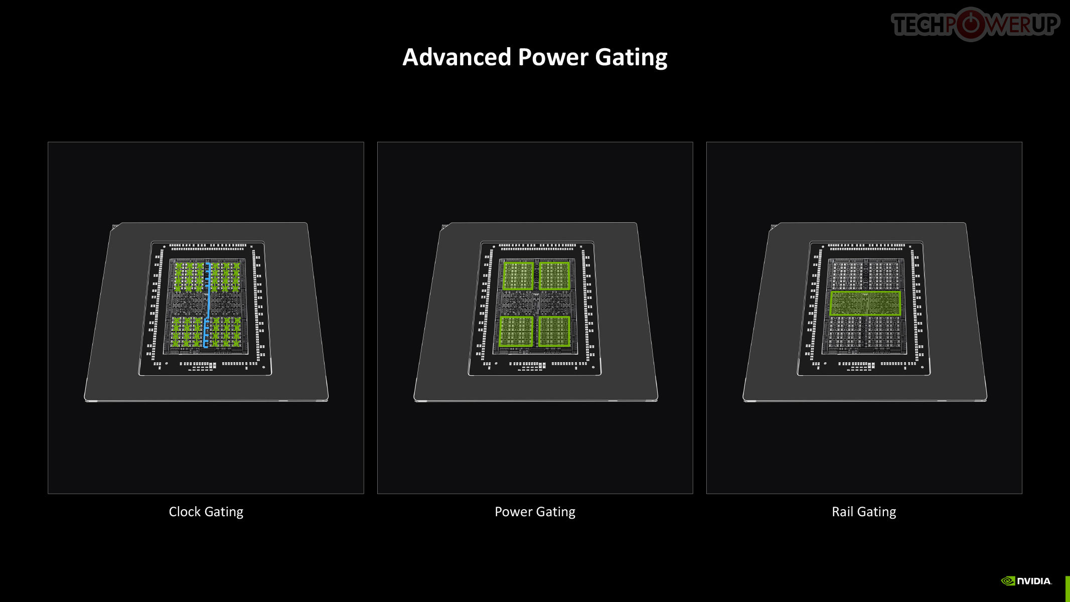
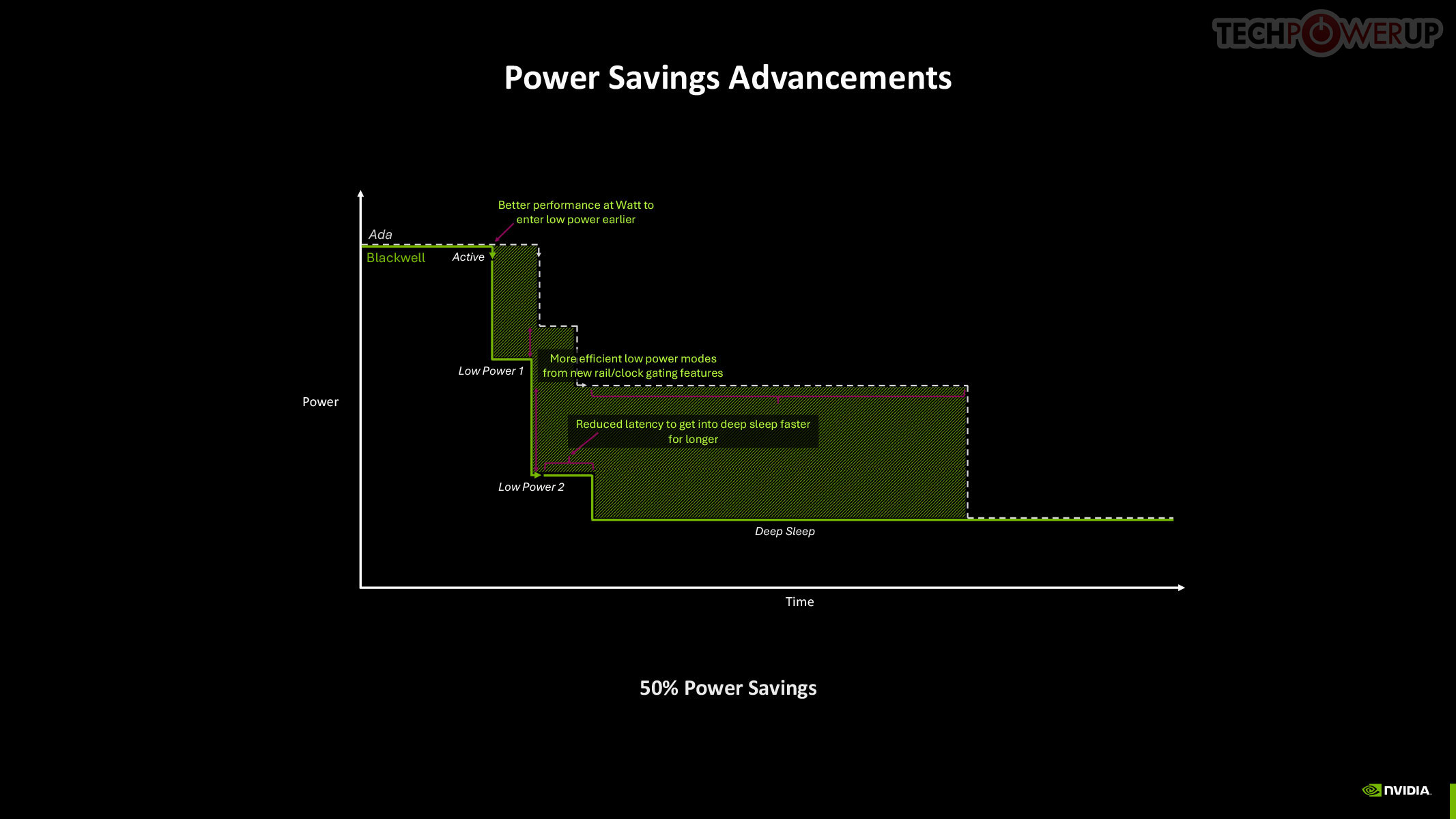
The GB202 and the rest of the GeForce Blackwell GPU family is built on the exact same TSMC "NVIDIA 4N" foundry node, which is actually 5 nm, as previous-generation Ada, so NVIDIA directed efforts to finding innovative new ways to manage power and thermals. This is done through a re-architected power management engine that relies on clock gating, power gating, and rail gating of the individual GPCs and other top-level components. It also worked on the speed at which the GPU makes power-related decisions.
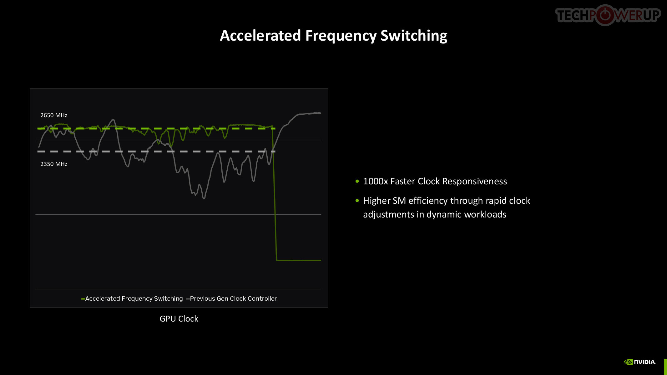
The quickest way to drop power is by adjusting the GPU clock speed, and with Blackwell, NVIDIA introduced a means for rapid clock adjustments at the SM-level.
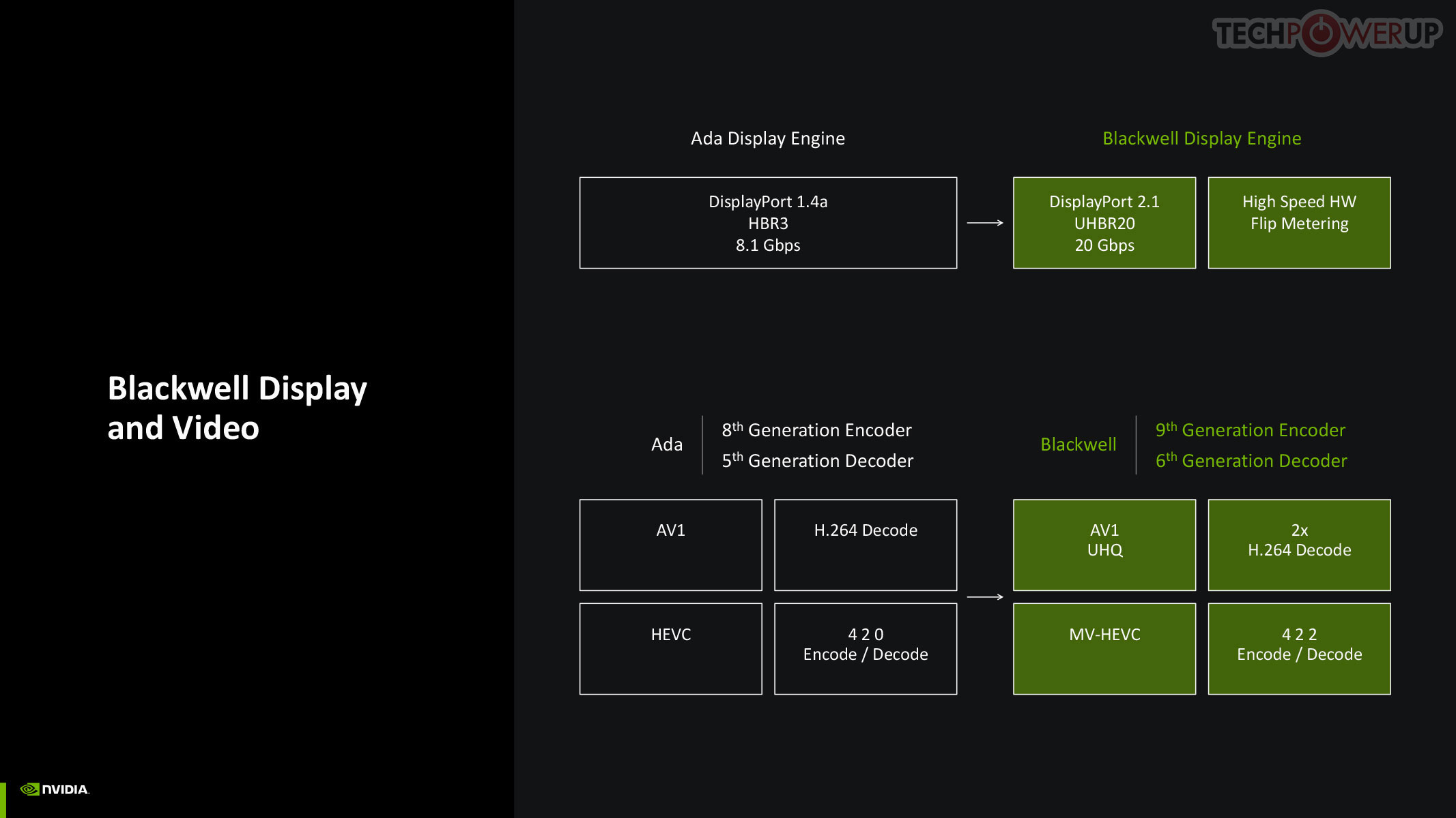
NVIDIA updated both the display engine and the media engine of Blackwell over the previous generation Ada, which drew some flack for holding on to older display I/O standards such as DisplayPort 1.4, while AMD and Intel had moved on to DisplayPort 2.1. The good news is that Blackwell supports DP 2.1 with UHBR20, enabling 8K 60 Hz with a single cable. The company also updated NVDEC and NVENC, which now support AV1 UHQ, double the H.264 decode performance, MV-HEVC, and 4:2:2 formats.
Neural Rendering
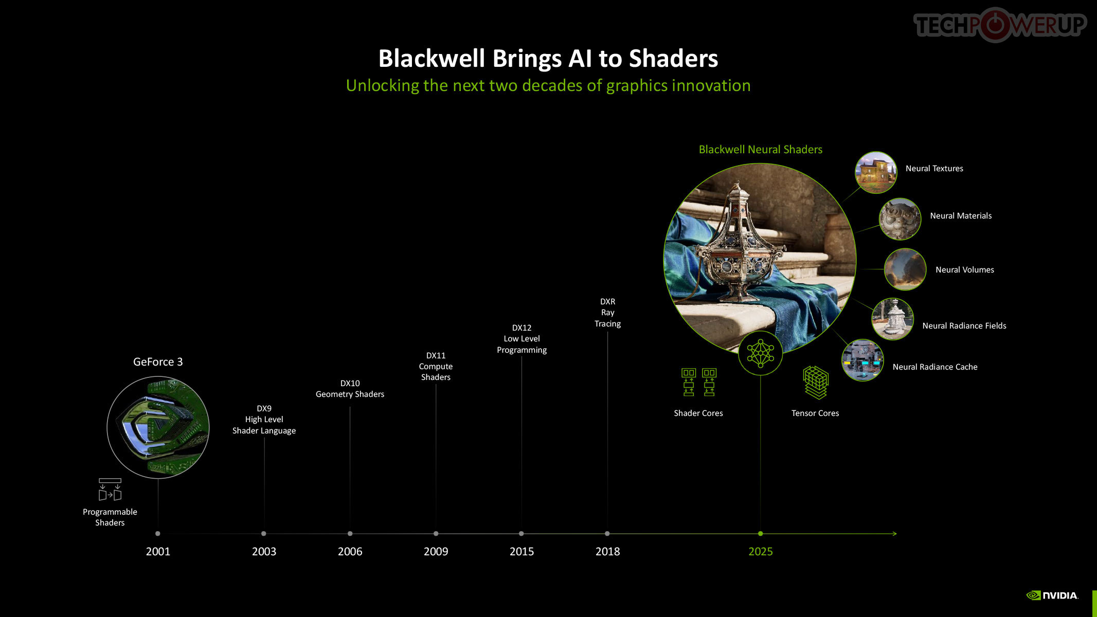
Neural Rendering promises to be as transformative to modern graphics as programmable shaders itself. 3D Graphics rendering evolved from fixed-function over the turn of the century, to programmable shaders, HLSL, geometry shaders, compute shaders, and ray tracing, over the past couple of decades. In 2025, NVIDIA is writing the next chapter in this journey with Blackwell neural shaders. This allows for a host of neural-driven effects, including neural materials, neural volumes, and even neural radiance fields. Microsoft introduced the new Cooperative Vectors API for DirectX in a recent update, making it possible to access Tensor cores within a graphics API. Combined with a new shading language, Slang, this breakthrough enables developers to integrate neural techniques directly into their workflows, potentially replacing parts of the traditional graphics pipeline. Slang splits large, complex functions into smaller pieces that are easier to handle. Given that this is a DirectX standard API feature, there is nothing that stops AMD and Intel from integrating Neural Rendering (Cooperative Vectors) into their graphics drivers.
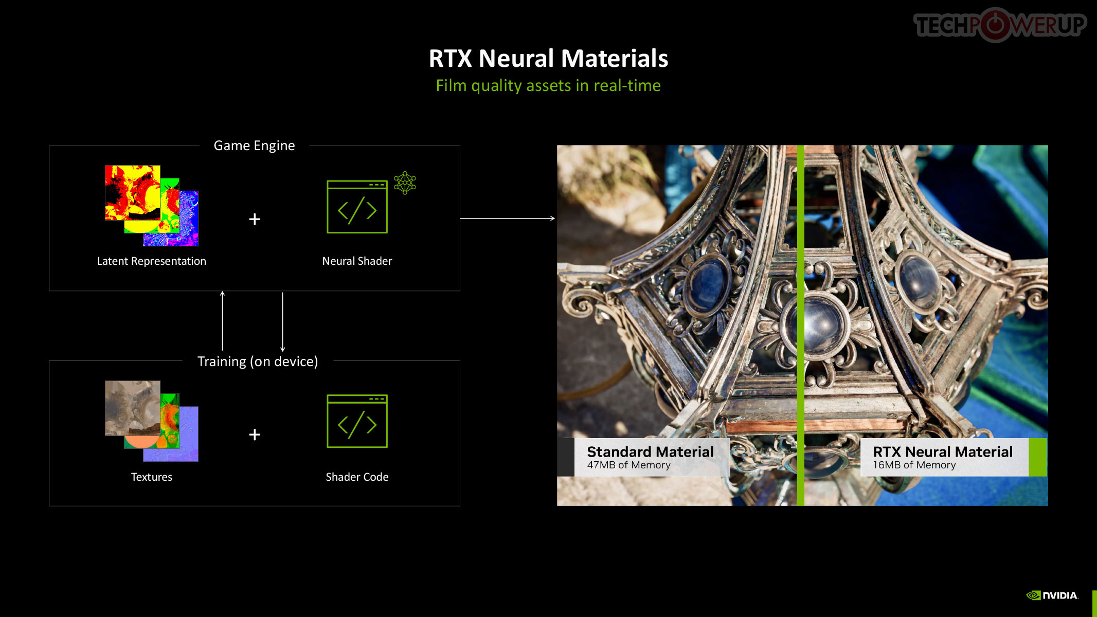
RTX Neural Materials works to significantly reduce the memory footprint of materials in 3D scenes. Under conventional rendering, the memory footprint of a material is bloated from complex shader code. Neural materials convert shader code and texture layers into a compressed neural representation. This results in up to a 7:1 compression ratio and enables small neural networks to generate stunning, film-like materials in real-time. For example, silk rendered with traditional shaders might lack the multicolored sheen seen in real life. Neural materials, however, capture intricate details like color variation and reflections, bringing such surfaces to life with unparalleled realism—and at a fraction of the memory cost.
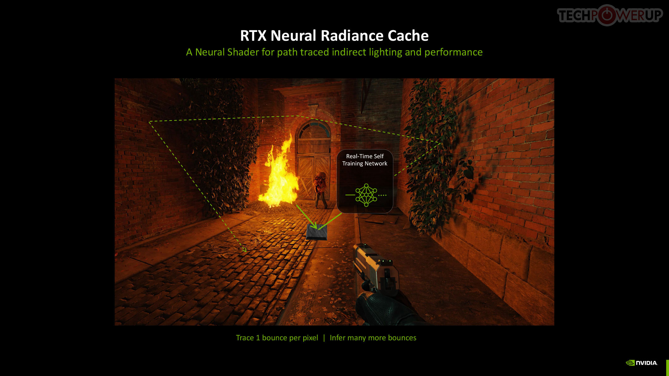
The new Neural Radiance Cache, which dynamically trains a neural network during gameplay using the user's GPU, allowing light transport to be cached spatially, enabling near-infinite light bounces in a scene. This results in realistic indirect lighting and shadows with minimal performance impact. NRC partially traces 1 or 2 rays before storing them in a radiance cache, and infers an infinite amount of rays and bounces for a more accurate representation of indirect lighting in the game scene.
DLSS 4 and Multi Frame Generation
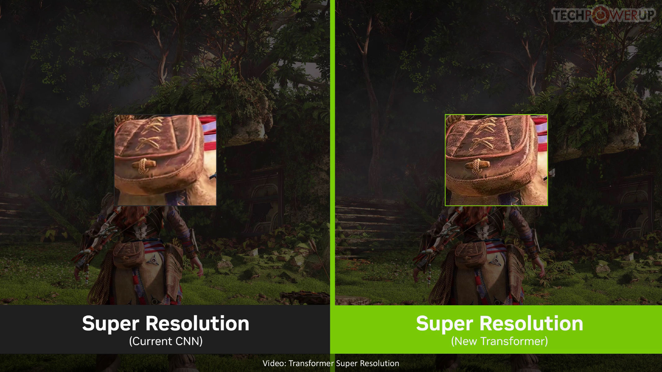
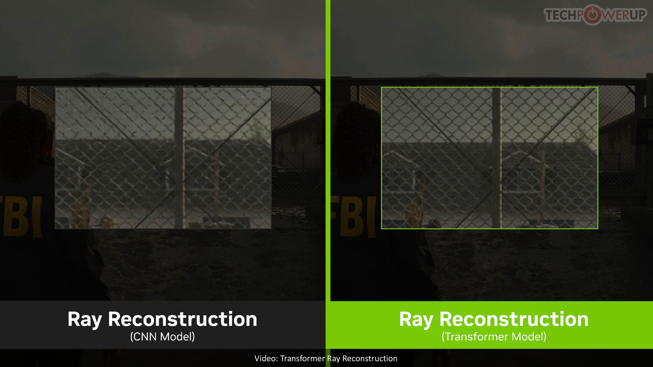
DLSS 4 introduces a major leap in image quality and performance. It isn't just a version bump with the introduction of a new feature, namely Multi Frame Generation, but introduces updates to nearly all DLSS sub-features. DLSS from its very beginning relied on AI to reconstruct details in super resolution, and with DLSS 4, NVIDIA is introducing a new transformer-based AI model to succeed the convolutional neural networks previous used, for double the parameters, four times the compute performance, and significantly improved image quality. Ray Reconstruction, introduced with DLSS 3.5, gets a significant image quality update with the new transformer-based model.
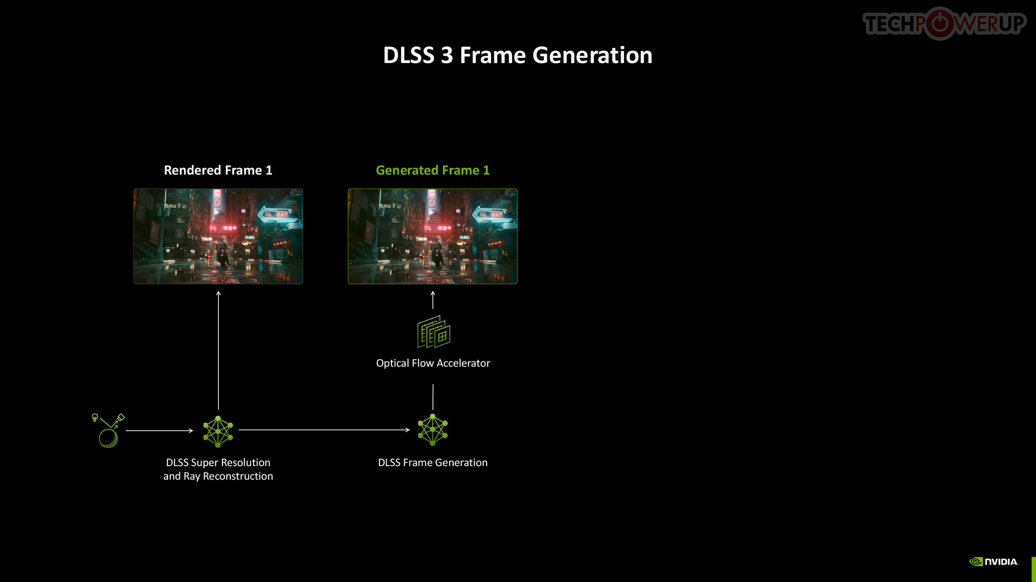
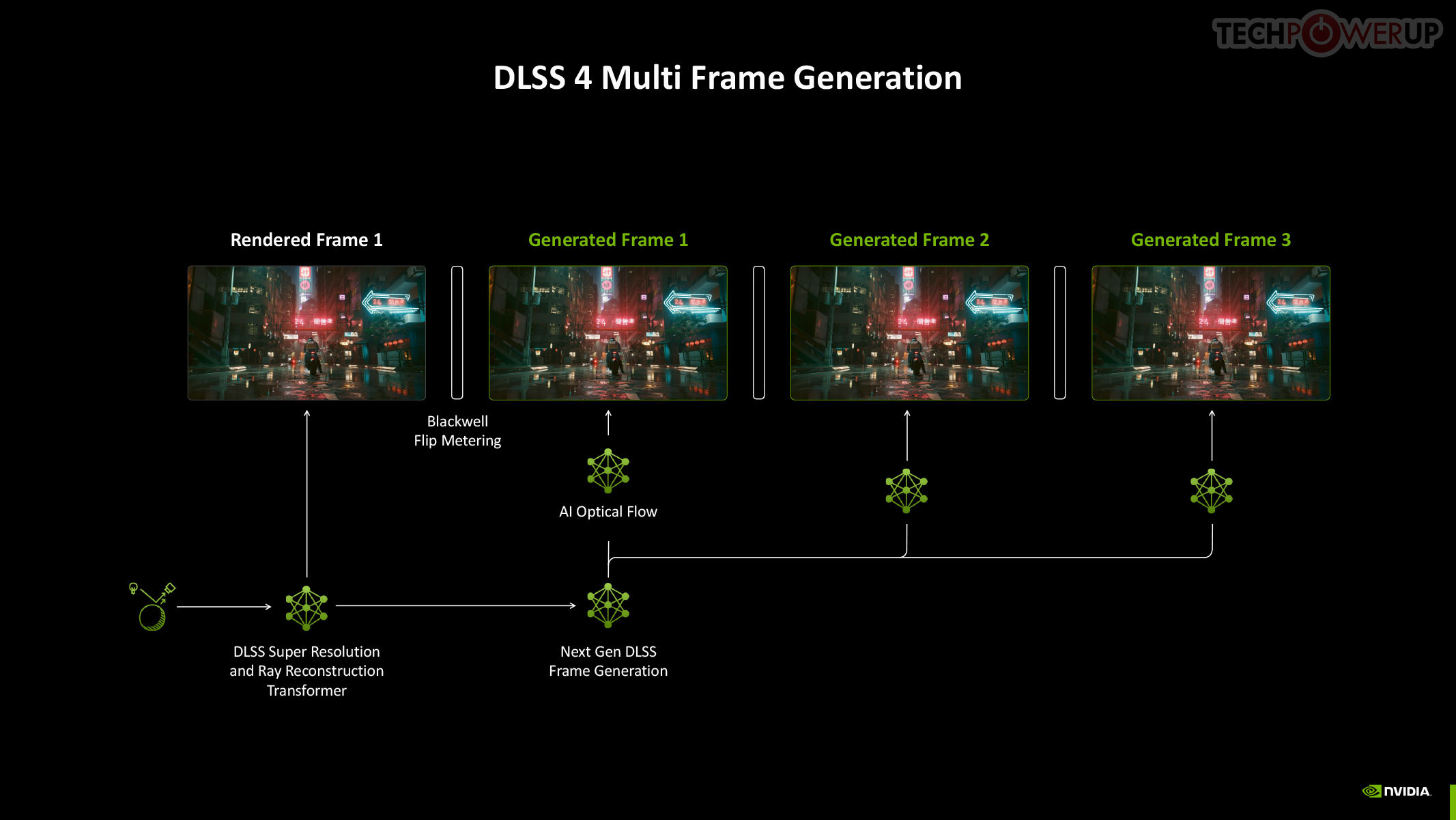
To understand Multi Frame Generation, you need to understand how DLSS Frame Generation, introduced with GeForce Ada, works. An Optical Flow Accelerator component gives the DLSS algorithm data to generate an entire frame using a neural network, using information from a previous rendered frame, effectively doubling frame rate. In Multi Frame Generation, AI takes over the functions of optical flow, to predict up to three frames following a conventionally rendered frame, effectively drawing four frames form the rendering effort of one.
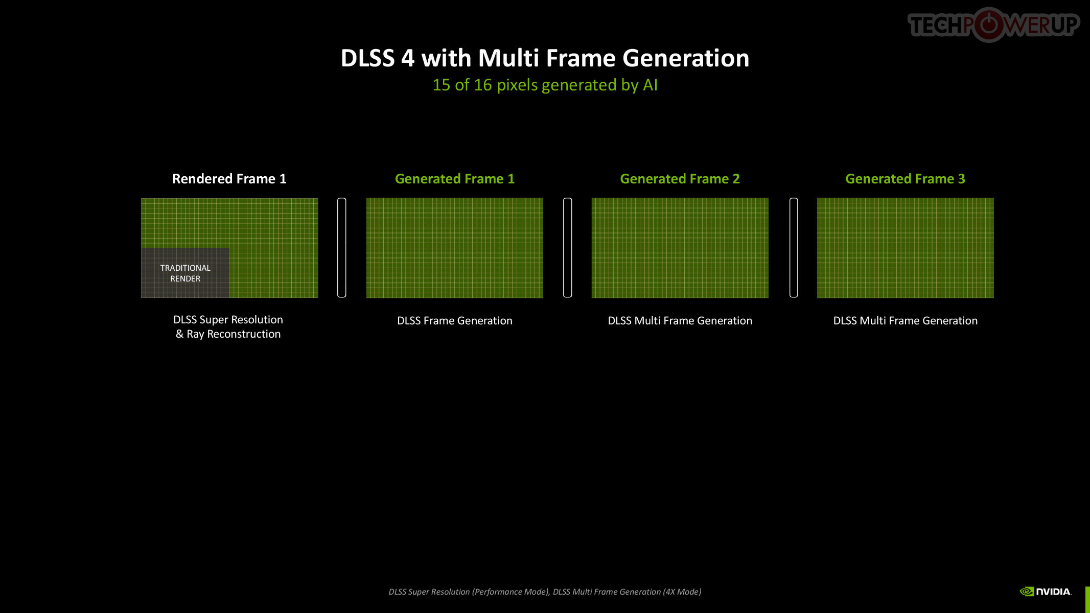
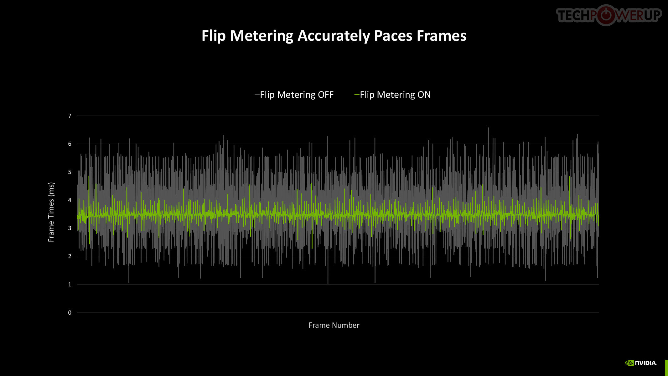
Now, assuming this rendered frame is a product of Super Resolution, with the maximum performance setting generating 4x the pixels from a single rendered pixel, you're looking at a possibility where the rendering effort of 1/4th a frame goes into drawing 4 frames, or 15 in every 16 pixels being generated entirely by DLSS. When generating so many frames, Frame Pacing becomes a problem—irregular frame intervals impact smoothness. DLSS 4 addresses these issues by using a dedicated hardware unit inside Blackwell, which takes care of flip metering, reducing frame display variability by 5-10x. The Display Engine of Blackwell contains the hardware for flip metering.
NVIDIA Reflex 2

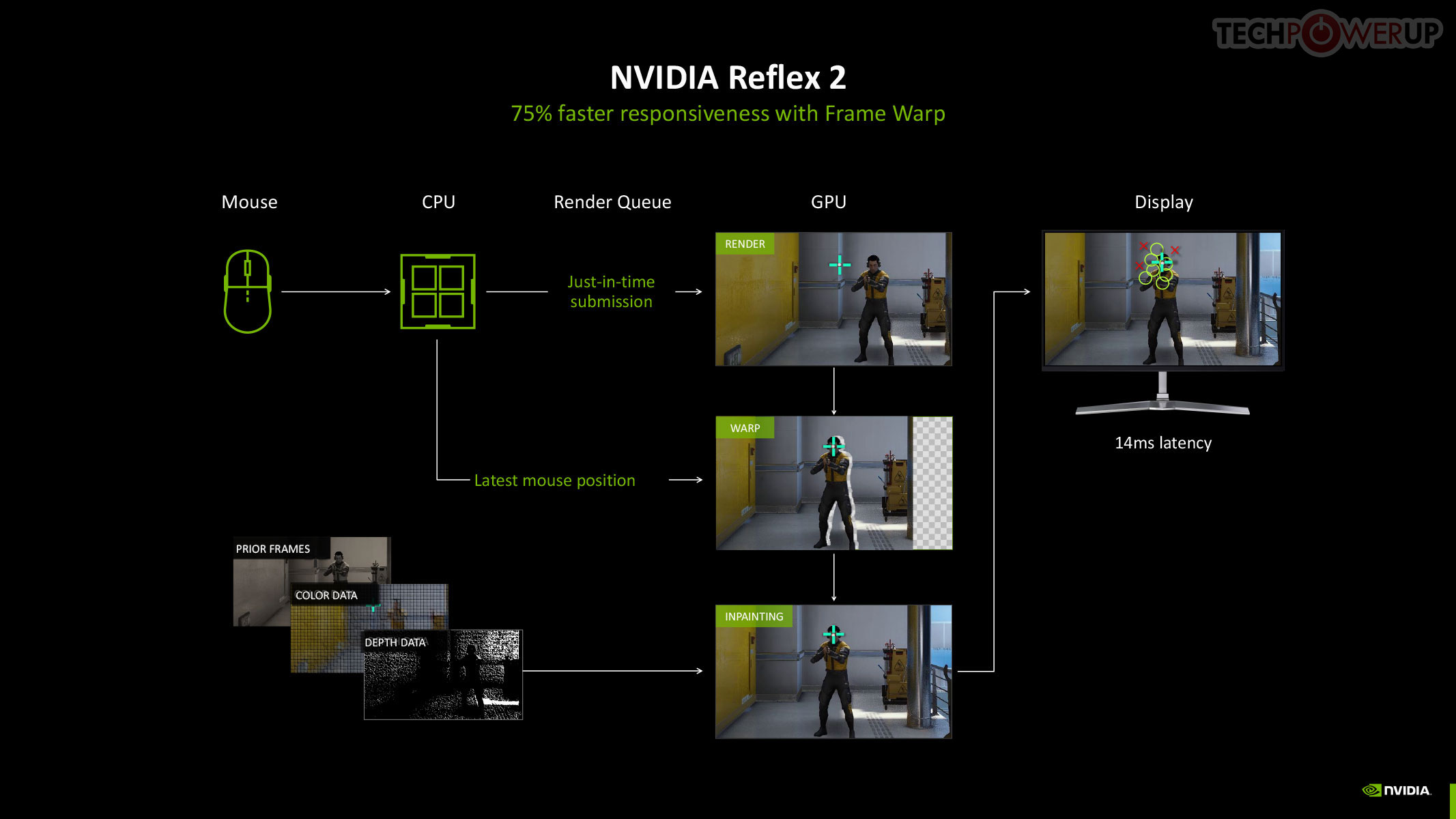
The original NVIDIA Reflex brought about a significant improvement to the responsiveness of maxed out graphics in competitive online gameplay, by compacting the rendering queue with the goal of reducing the whole system latency by up to 50%. Reflex is mandatory in DLSS 3 Frame Generation, given the latency cost imposed by the technology. Multi-frame generation calls for an equally savvy piece of technology, so we hence have Reflex 2. NVIDIA claims to have achieved a 75% reduction in latency with Frame Warp, which updates the camera (viewport) positions based on user inputs in real-time, and then uses temporal information to reconstruct the frame to display.
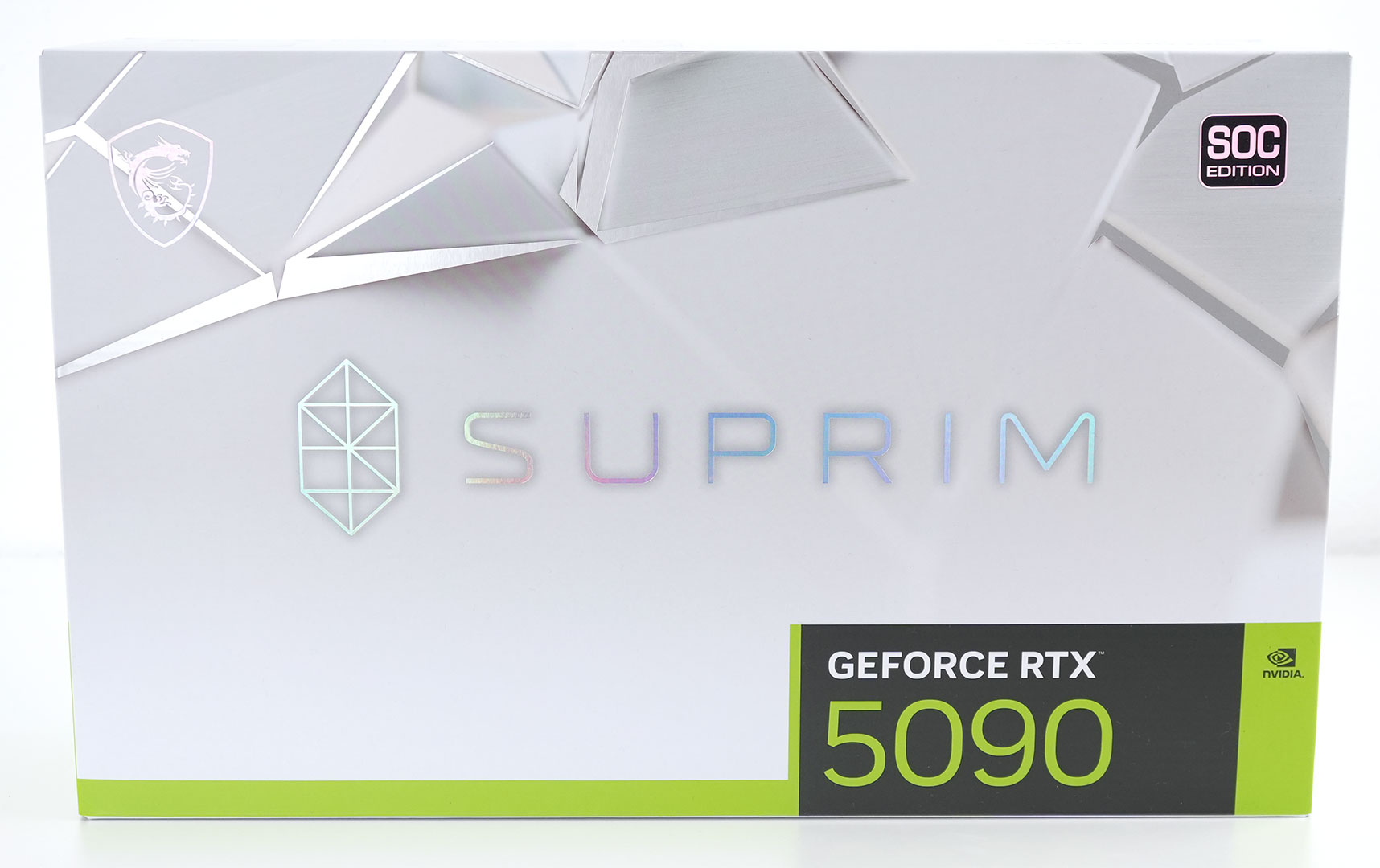
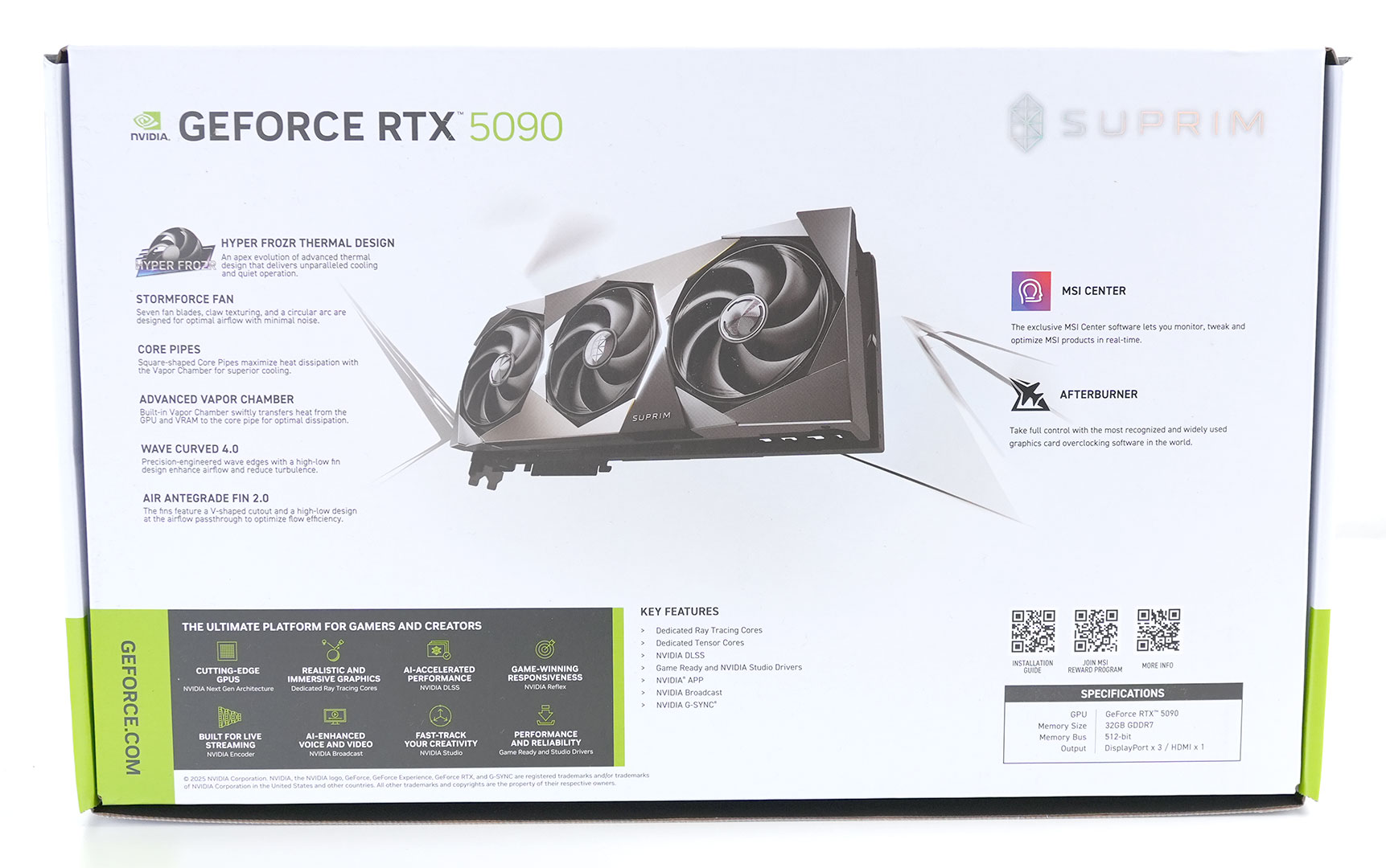
Packaging
The Card
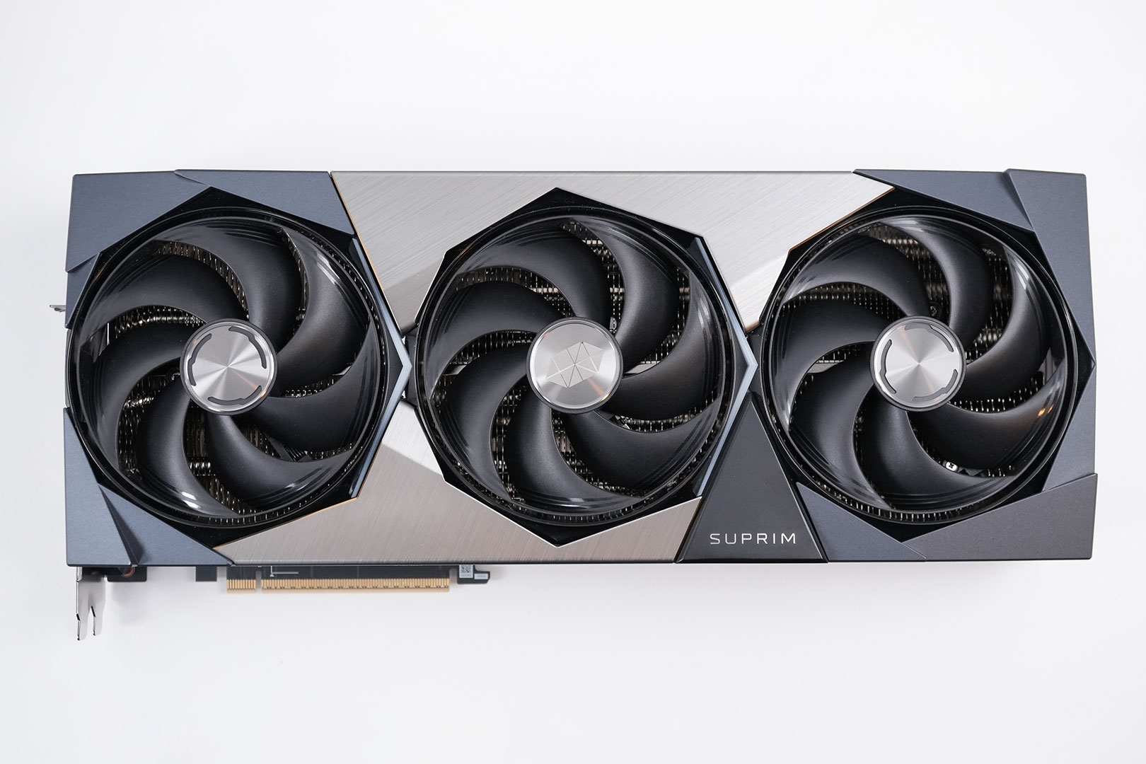
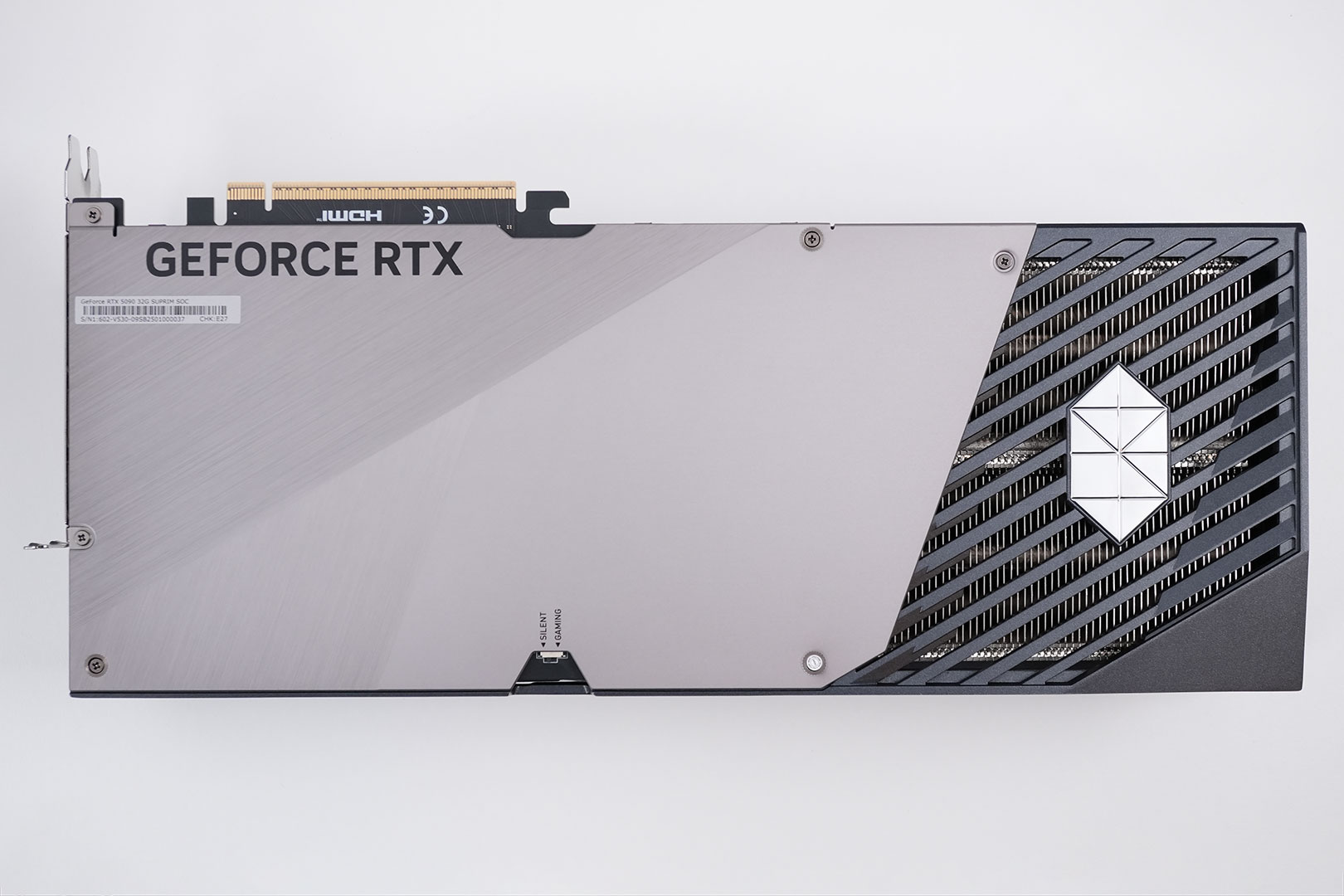
MSI follows the design theme of their GeForce 40 Suprim lineup—metal silver with gray highlights is the name of the game. On the back you get a metal backplate with a cutout for air to flow through.
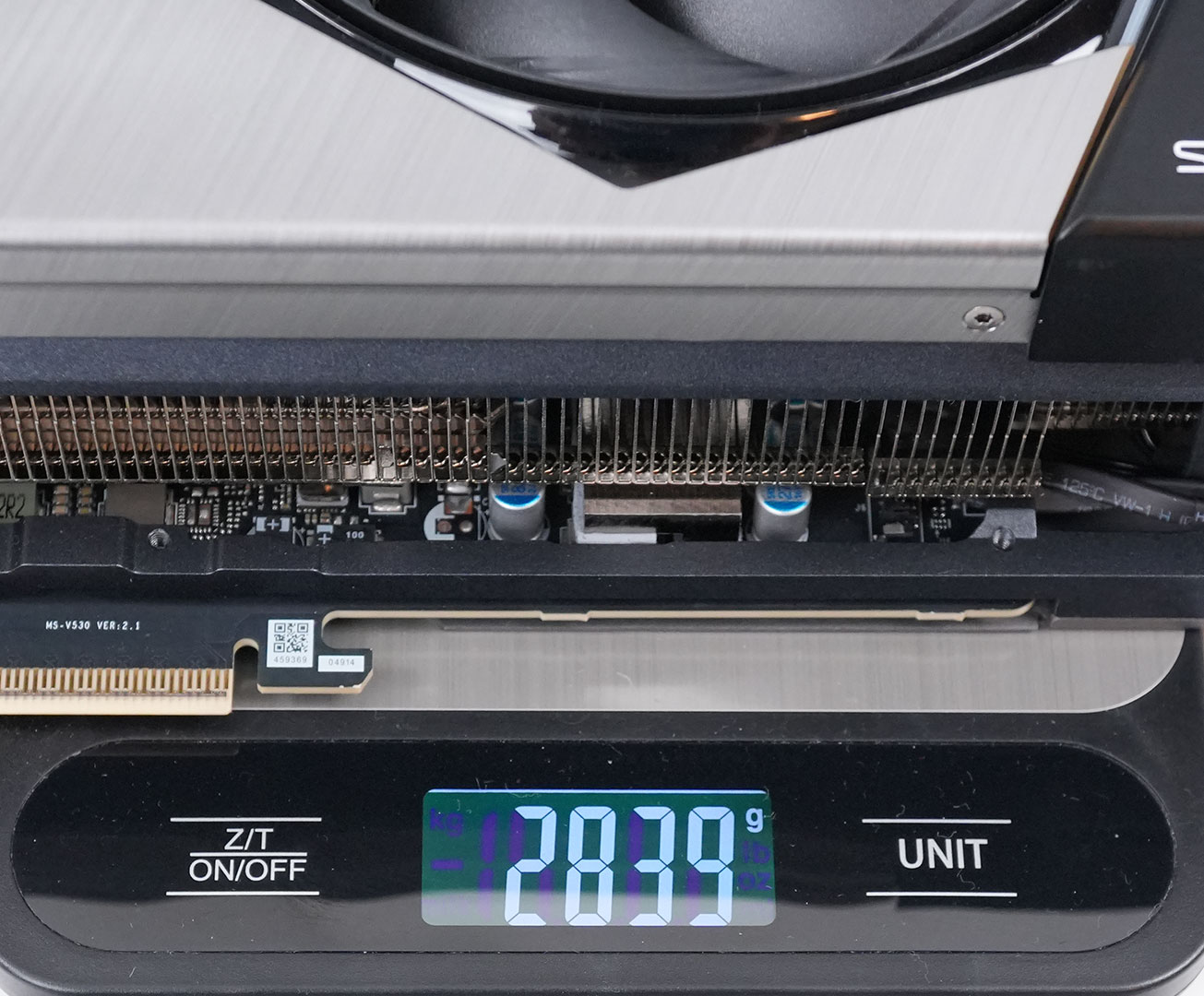
Dimensions of the card are 36.0 x 15.0 cm, and it weighs 2839 g.
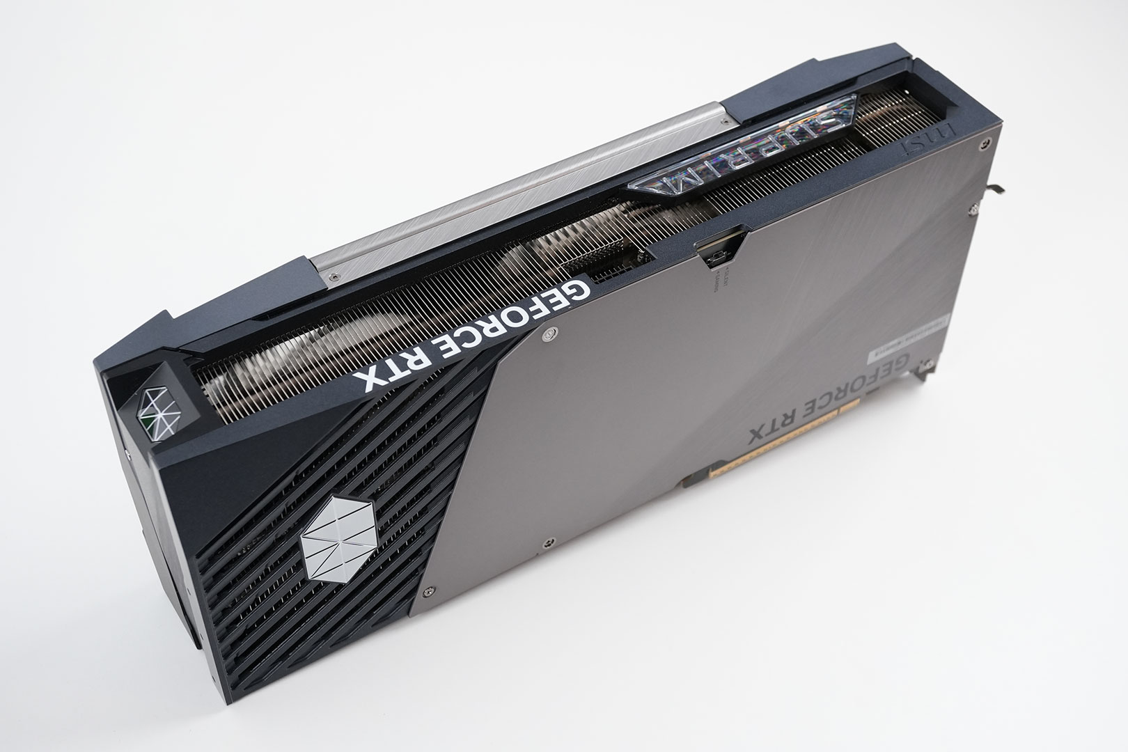
Installation requires four slots in your system. We measured the card's width to be 75 mm.
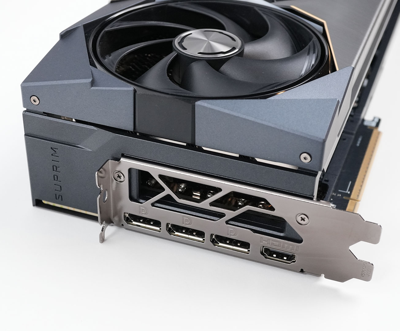
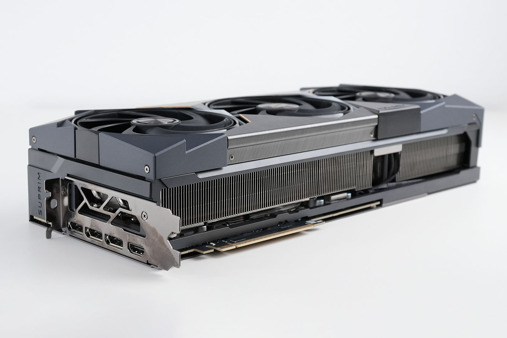
Display connectivity includes three standard DisplayPort 2.1b and one HDMI 2.1b.
Standard for all GeForce RTX 50-series Blackwell cards is a new display engine that supports three DisplayPort 2.1b outputs, each capable of UHBR20; and one HDMI 2.1a. Both interfaces support DSC (display stream compression). With DSC enabled, a single DisplayPort on this card can drive 4K 12-bit HDR at 480 Hz; or 8K 12-bit HDR at up to 165 Hz. The RTX 5090 features an updated media acceleration engine with support for 4:2:2 video formats, AV1 UHQ, and MV-HEVC. There are three independent NVENC units, and two NVDEC.
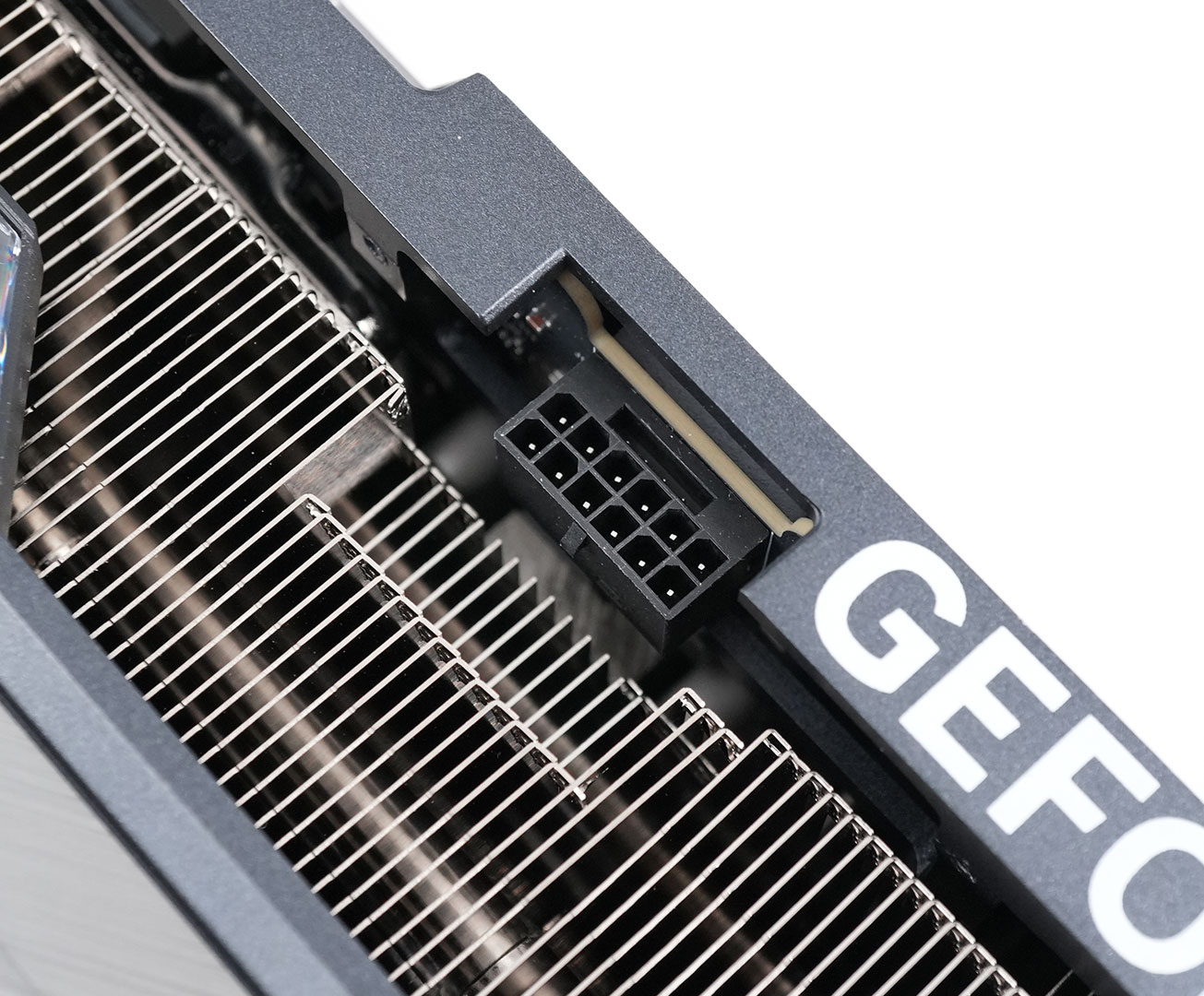
The card uses a single 16-pin connector, which allows a maximum power draw of 600 W.
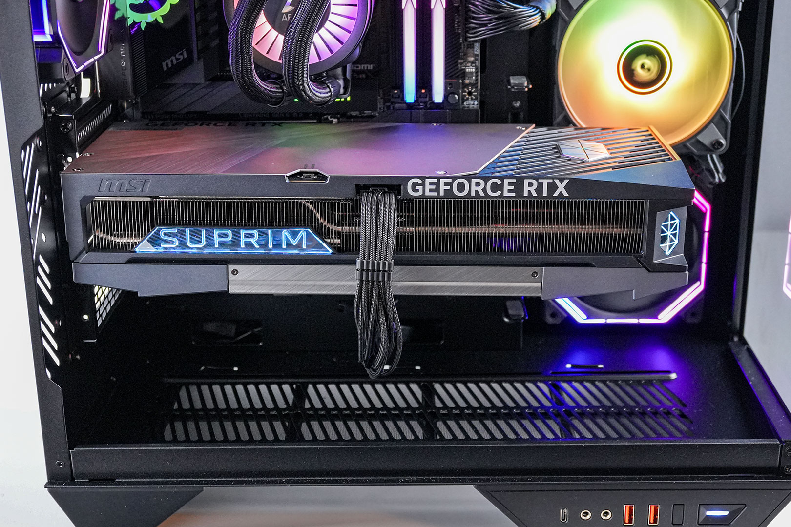
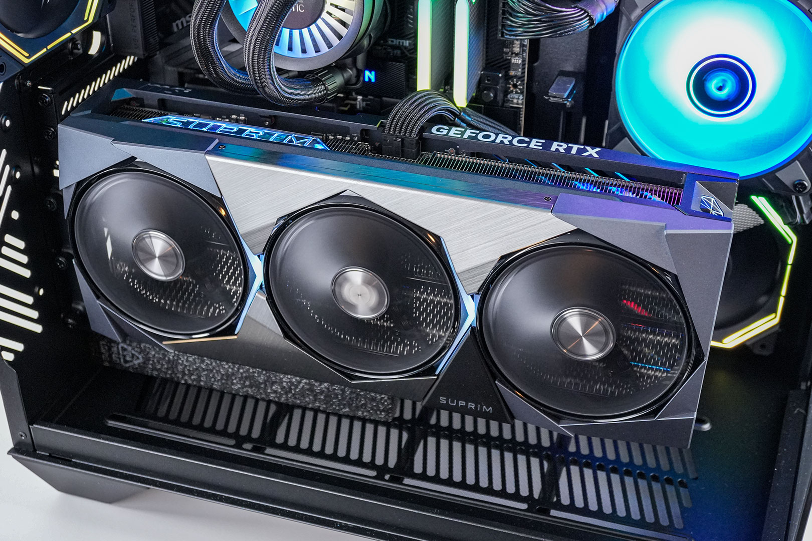
MSI has installed adjustable RGB lighting zones near the fans, the Suprim text logo is illuminated and the Suprim logo on the corner, too.
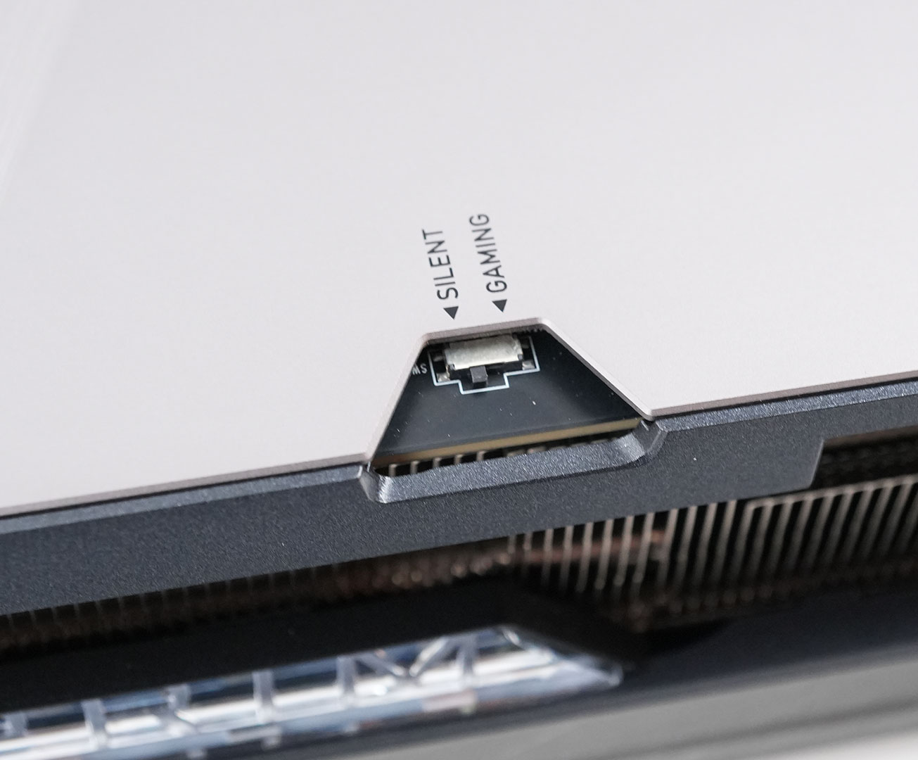
This dual BIOS switch lets you toggle between the default "silent" BIOS and a "gaming" BIOS with a more aggressive fan curve. The Gaming BIOS will also increase the default power limit to 600 W (up from 575 W).
Our Patreon Silver Supporters can read articles in single-page format.
Apr 24th, 2025 14:11 EDT
change timezone
Latest GPU Drivers
New Forum Posts
- New GPU 5070 Ti or better CPU Ryzen7 7800X3D ? (19)
- I dont understand the phone OS world..... (34)
- New OLED monitor makes PC unresponsive sometimes (2)
- Waterloop 24/7 or no? (18)
- Choosing an Internal HDD (4)
- Companies should be called out for this (91)
- Are the 8 GB cards worth it? (160)
- To distill or not distill what say ye? (99)
- Do you use Linux? (592)
- 5060 Ti 8GB DOA (265)
Popular Reviews
- NVIDIA GeForce RTX 5060 Ti 8 GB Review - So Many Compromises
- Colorful iGame B860M Ultra V20 Review
- ASUS GeForce RTX 5060 Ti TUF OC 16 GB Review
- ASRock X870E Taichi Lite Review
- Upcoming Hardware Launches 2025 (Updated Apr 2025)
- Sapphire Radeon RX 9070 XT Pulse Review
- Sapphire Radeon RX 9070 XT Nitro+ Review - Beating NVIDIA
- Crucial CUDIMM DDR5-6400 128 GB CL52 Review
- AMD Ryzen 7 9800X3D Review - The Best Gaming Processor
- NVIDIA GeForce RTX 5060 Ti PCI-Express x8 Scaling
Controversial News Posts
- NVIDIA GeForce RTX 5060 Ti 16 GB SKU Likely Launching at $499, According to Supply Chain Leak (182)
- NVIDIA Sends MSRP Numbers to Partners: GeForce RTX 5060 Ti 8 GB at $379, RTX 5060 Ti 16 GB at $429 (127)
- NVIDIA Launches GeForce RTX 5060 Series, Beginning with RTX 5060 Ti This Week (115)
- Nintendo Confirms That Switch 2 Joy-Cons Will Not Utilize Hall Effect Stick Technology (105)
- Nintendo Switch 2 Launches June 5 at $449.99 with New Hardware and Games (99)
- Sony Increases the PS5 Pricing in EMEA and ANZ by Around 25 Percent (85)
- NVIDIA PhysX and Flow Made Fully Open-Source (77)
- Windows Notepad Gets Microsoft Copilot Integration (75)