 355
355
NVIDIA GeForce RTX 3080 Founders Edition Review - Must-Have for 4K Gamers
(355 Comments) »Introduction
Ampere is here! We have with us in this comprehensive performance review the NVIDIA GeForce RTX 3080 Founders Edition graphics card. NVIDIA shook things up early this month by announcing not just the RTX 3080, but also the larger RTX 3090 and more affordable RTX 3070. Curiously, the GeForce RTX 3080 is being labeled as a "flagship product," while the RTX 3090 is being extensively compared to past-generation TITAN cards. With a starting price of $699, the RTX 3080 is designed to offer 4K UHD gameplay at frame-rates in excess of 60 FPS, 100+ FPS at 1440p, and extreme refresh-rate (360 Hz) gameplay.
The Ampere architecture, which we extensively detailed in our dedicated NVIDIA Ampere architecture article, heralds the 2nd generation of NVIDIA's path-breaking RTX real-time raytracing technology, with a design goal of making RTX go above and beyond the DirectX Raytracing feature set, and for raytracing to have as little impact on game playability as possible. With the new RTX 3080 and RTX 3090, NVIDIA is also introducing a new dual axial flow through cooling solution, which we detailed in our RTX 3080 Unboxing & Preview article from last week. To make this design work, NVIDIA also introduced an all new 12-pin power input, which we hope becomes a standard going forward.
The "Ampere" architecture itself debuted in Spring 2020 as part of the A100 Tensor Core scalar HPC processor targeted at AI DNN researchers. As a consumer graphics architecture, "Ampere" is debuting today, and our first coverage is this GeForce RTX 3080 Founders Edition review. The A100 Tensor Core processor has certain architectural bits that aren't relevant to the gaming segment, such as FP64 cores and HBM2E memory, and completely lacks all raster graphics machinery, which is required for gaming. The GeForce "Ampere" architecture does away with FP64 cores, has a supremely modernized raster hardware components, and new 2nd generation RT cores. What's common between the two are the awesome new 3rd generation Tensor cores that leverage sparsity to increase AI inference performance by an order of magnitude; and the new "Ampere" FP32 CUDA core with more efficient utilization of its number-crunching machinery.

NVIDIA has over the past decade perfected the art of presenting GeForce graphics cards as not just pieces of hardware, but complete consumer graphics solutions with software features that enhance the PC gaming experience. The company finds itself as a bulwark platform of PC gaming while the gaming experience on consoles is getting closer to the PC than ever. With new-generation Xbox and PlayStation consoles promising 4K UHD gaming, NVIDIA probably feels PC gaming can only survive if it maintains a vast technological superiority that translates into an experience that's proportionately superior. This appears to be the main reason behind the company's push toward real-time raytracing. While fully raytraced rendering continues to remain theoretical in consumer use cases, NVIDIA figured out a way to compose conventional raster 3D graphics with cleverly raytraced elements (such as lighting, shadows, reflections, and more). With the second generation of RTX, NVIDIA is adding more true-to-life effects, such as raytraced motion blur. The company even designed special hardware just for this effect!
NVIDIA is also sending the message that GeForce "Ampere" represents "the best of next-gen," and wants to show that merely being first to market with something doesn't automatically make the product superior. The "GA102" chip at the heart of the RTX 3080 Founders Edition is built on the new 8 nm silicon fabrication node by Samsung, offering comparable transistor densities and iso-power to TSMC 7 nm. It also implements PCI-Express Gen 4 for better IO connectivity with the latest desktop platforms, such as 3rd Gen Ryzen and the upcoming Intel Core processors. In the separate NVIDIA RTX 3080 PCI-Express Scaling article, we will take a closer look at the bus interface, and in yet another article, we compare the RTX 3080 on similarly priced premium processors by Intel and AMD, with the RTX 3080 benchmarked on the Core i9-10900K vs. the Ryzen 9 3900XT.
The NVIDIA GeForce RTX 3080 Founders Edition feels like a piece of jewelry in hand. That's because NVIDIA has for the past many generations stopped looking at its reference design products as baselines set for its board partners to improve upon, as they are, rather, high engineering standards their partners can aspire to meet or exceed with custom-design products. This is why NVIDIA refrains from using the term "reference design" when talking about Founders Edition products. Unlike the previous-generation RTX 2080 Founders Edition, which came at a premium price above the starting price, the new RTX 3080 Founders Edition will be launched at the $699 price. In this review, we take the GeForce RTX 3080 Founders Edition for a spin across our updated test suite of real world gaming benchmarks. We also explore the card's unique new design in detail by disassembling it, and test the card's new thermal and electrical features.
Our NVIDIA GeForce RTX 3080 Founders Edition launch-day coverage includes:
- The NVIDIA GeForce RTX 3080 Founders Edition main review (this review)
- NVIDIA GeForce RTX 3080 with AMD Ryzen 3900XT vs Intel Core i9-10900K
- NVIDIA GeForce RTX 3080 PCI-Express Scaling
- NVIDIA GeForce Ampere Architecture, Board Design, Gaming Tech & Software (last week)
- NVIDIA GeForce RTX 3080 Unboxing (last week)
| Price | Shader Units | ROPs | Core Clock | Boost Clock | Memory Clock | GPU | Transistors | Memory | |
|---|---|---|---|---|---|---|---|---|---|
| GTX 1080 Ti | $650 | 3584 | 88 | 1481 MHz | 1582 MHz | 1376 MHz | GP102 | 12000M | 11 GB, GDDR5X, 352-bit |
| RX 5700 XT | $370 | 2560 | 64 | 1605 MHz | 1755 MHz | 1750 MHz | Navi 10 | 10300M | 8 GB, GDDR6, 256-bit |
| RTX 2070 | $340 | 2304 | 64 | 1410 MHz | 1620 MHz | 1750 MHz | TU106 | 10800M | 8 GB, GDDR6, 256-bit |
| RTX 2070 Super | $450 | 2560 | 64 | 1605 MHz | 1770 MHz | 1750 MHz | TU104 | 13600M | 8 GB, GDDR6, 256-bit |
| Radeon VII | $680 | 3840 | 64 | 1802 MHz | N/A | 1000 MHz | Vega 20 | 13230M | 16 GB, HBM2, 4096-bit |
| RTX 2080 | $600 | 2944 | 64 | 1515 MHz | 1710 MHz | 1750 MHz | TU104 | 13600M | 8 GB, GDDR6, 256-bit |
| RTX 2080 Super | $690 | 3072 | 64 | 1650 MHz | 1815 MHz | 1940 MHz | TU104 | 13600M | 8 GB, GDDR6, 256-bit |
| RTX 2080 Ti | $1000 | 4352 | 88 | 1350 MHz | 1545 MHz | 1750 MHz | TU102 | 18600M | 11 GB, GDDR6, 352-bit |
| RTX 3070 | $500 | 5888 | 96 | 1500 MHz | 1725 MHz | 1750 MHz | GA104 | 17400M | 8 GB, GDDR6, 256-bit |
| RTX 3080 | $700 | 8704 | 96 | 1440 MHz | 1710 MHz | 1188 MHz | GA102 | 28000M | 10 GB, GDDR6X, 320-bit |
| RTX 3090 | $1500 | 10496 | 112 | 1395 MHz | 1695 MHz | 1219 MHz | GA102 | 28000M | 24 GB, GDDR6X, 384-bit |
The GeForce Ampere Architecture
Earlier this month, on September 5, we did a comprehensive article on the NVIDIA GeForce Ampere graphics architecture, along with a deep-dive into the key 2nd Gen RTX technology and various other features NVIDIA is introducing that are relevant to gaming. Be sure to check out that article for more details.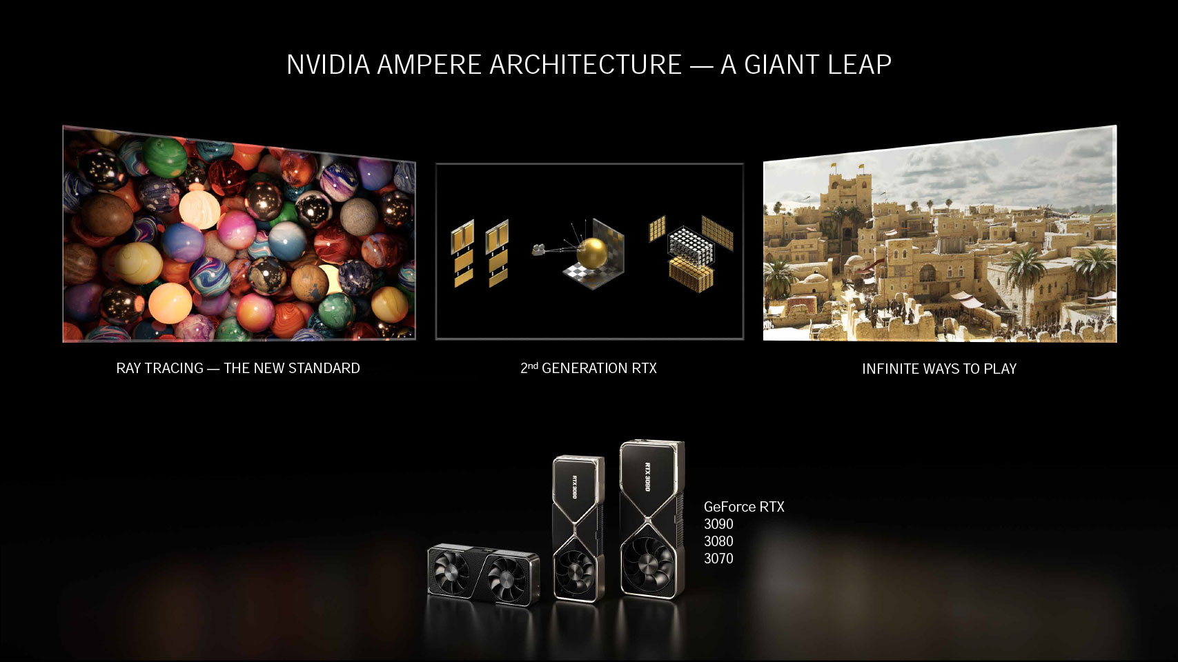

The GeForce Ampere architecture is the first time NVIDIA both converged and diverged its architecture IP between graphics and compute processors. Back in May, NVIDIA debuted Ampere on its A100 Tensor Core compute processor targeted at AI and HPC markets. The A100 Tensor Core is a headless compute chip that lacks all raster graphics components, so NVIDIA could cram in the things relevant to the segment. The GeForce Ampere, however, is a divergence, with a redesigned streaming multiprocessor different from that of the A100. These chips have all the raster graphics hardware, display and media acceleration engines, and, most importantly, the 2nd generation RT core that accelerates real-time raytracing. A slightly slimmed down version of the 3rd generation tensor core of the A100 also gets carried over. NVIDIA sticks to using GDDR-type memory over expensive memory architectures, such as HBM2E. Memory sizes have been increased generation over generation, as well as memory bus widths, but NVIDIA also worked with Micron Technology to introduce a new non-JEDEC memory type it calls GDDR6X, which increases data rates by over 20 percent over GDDR6.
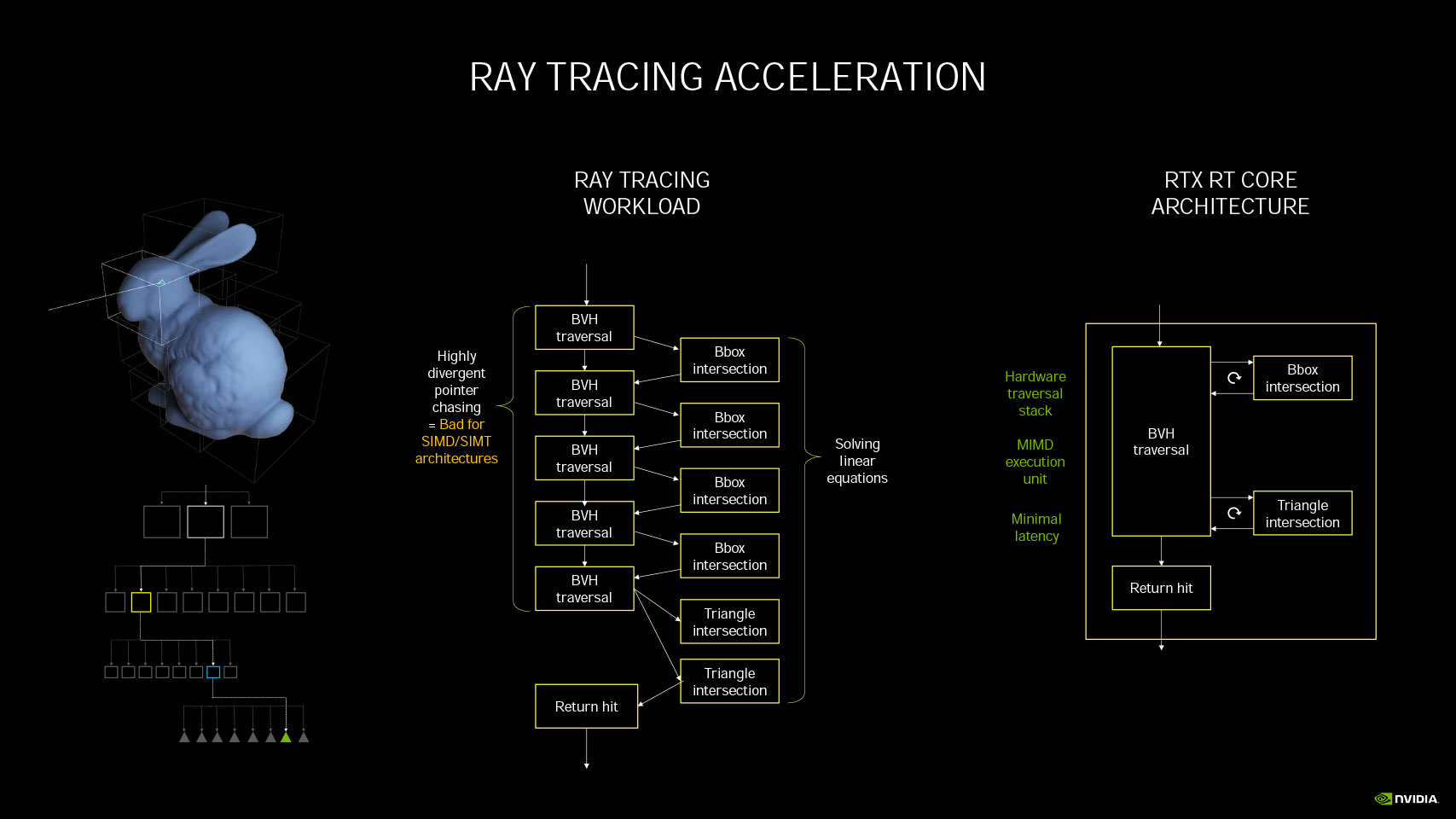
NVIDIA pioneered real-time raytracing on consumer graphics hardware, and three key components make the NVIDIA RTX technology work: the SIMD components, aka CUDA cores, the RT cores, which do the heavy lifting with raytracing, calculating BVH traversal, and intersections, and tensor cores, which are hardware component accelerating AI deep-learning neural net building, and training. NVIDIA uses an AI-based denoiser for RTX. With Ampere, NVIDIA is introducing new generations of the three components, with the objective being to reduce the performance cost of RTX, and nearly double performance over generations. These include the new Ampere streaming multiprocessor that more than doubles FP32 throughput over generations, the 2nd Gen RT core that features hardware that enables new RTX effects, such as raytraced motion blur, and the 3rd generation tensor core, which leverages sparsity in DNNs to increase AI inference performance by an order of magnitude.
GA102 GPU and Ampere SM


NVIDIA is taking a new approach to segmenting its high-end graphics cards with this generation. While the RTX 2080 and RTX 2080 Ti from the past generation were based on two different pieces of silicon—the TU104 and TU102 respectively—the new RTX 3080 and upcoming RTX 3090 are based a common silicon, the GA102, which is the biggest based on the GeForce Ampere architecture. The GA102 is based on the new Samsung 8N silicon fabrication process, an 8 nm node Samsung specially designed for NVIDIA, offering comparable transistor densities and iso-power to TSMC's 7 nm-class nodes. This large 628.4 mm² piece of silicon crams in 28.3 billion transistors.
The GA102 silicon features a largely similar component hierarchy to past-generation NVIDIA GPUs, but with the bulk of engineering effort focused on the new Ampere Streaming Multiprocessor (SM). The GPU supports the PCI-Express 4.0 x16 host interface, which doubles the host interface bandwidth over PCI-Express 3.0 x16. In today's GeForce RTX 3080 PCI-Express Scaling article, we test whether the RTX 3080 can actually benefit from PCIe Gen 4. With this generation, NVIDIA is also relegating SLI and the NVLink interface to only the top-dog RTX 3090, even the RTX 3080 loses out on it. With the past generation, even the RTX 2070 Super had NVLink. The decision to use a common silicon between the RTX 3080 and RTX 3090 may have had a lot to do with the memory bandwidth target. The RTX 3080 is endowed with a 320-bit wide memory interface, which is wider than the 256-bit interface of the RTX 2080.
The GA102 silicon features seven graphics processing clusters (GPCs), the mostly independent subunits of the GPU, from which one GPC is completely disabled on the RTX 3080. Each GPC has six texture processing clusters (TPCs), the indivisible subunit that is the main number-crunching muscle of the GPU. In addition to a whole GPC, two random TPCs are disabled from the remaining six GPCs to carve out the RTX 3080. Each TPC shares a PolyMorph engine between two streaming multiprocessors (SMs). The SM is what defines the generation and where the majority of NVIDIA's engineering effort is localized. The Ampere SM crams in 128 CUDA cores, double that of the 64 CUDA cores in the Turing SM.


Each GeForce Ampere SM features four processing blocks that each share an L1I cache, warp scheduler, and a register file among 128 CUDA cores. From these, 64 can handle concurrent FP32 and INT32 math operations, while 64 are pure FP32. Each cluster also features a 3rd generation Tensor Core. At the SM level, the four processing blocks share a 128 KB L1D cache that also serves as shared memory; four TMUs and a 2nd generation RT core. As we mentioned, each processing block features two FP32 data paths; one of these consists of CUDA cores that can execute 16 FP32 operations per clock cycle, while the other data path consists of CUDA cores capable of 16 FP32 and 16 INT32 concurrent operations per clock. Each SM also features a tiny, unspecified number of rudimentary FP64 cores, which work at 1/64 the performance of the FP64 cores on the A100 Tensor Core HPC processor. These FP64 cores are only there so double-precision software doesn't run into compatibility problems.
2nd Gen RT Core, 3rd Gen Tensor Core

NVIDIA's 2nd generation RTX real-time raytracing technology sees the introduction of more kinds of raytraced effects. NVIDIA's pioneering technology involves composing traditional raster 3D scenes with certain raytraced elements, such as lighting, shadows, global illumination, and reflections.
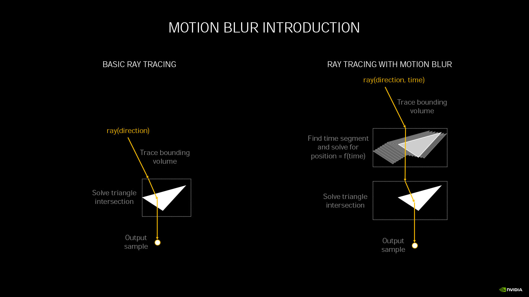

As explained in the Ampere Architecture article, NVIDIA's raytracing philosophy involves heavy bounding volume hierarchy (BVH) traversal, and bounding box/triangle intersection, for which NVIDIA developed specialized MIMD fixed function in the RT core. Fixed-function hardware handles both traversal and intersection of rays with bounding boxes or triangles. With the 2nd Gen RT core, NVIDIA is introducing a new component which interpolates triangle position by time. This component enables physically accurate, raytraced motion-blur. Until now, motion-blur was handled as a post-processing effect.


The 3rd generation tensor core sees NVIDIA build on the bulwark of its AI performance leadership, fixed-function hardware designed for tensor math, which accelerates AI deep-learning neural-net building and training. AI is heavily leveraged in NVIDIA architectures now, as the company uses an AI-based denoiser for its raytracing architecture, and to accelerate technologies such as DLSS. Much like the 3rd generation tensor cores on the company's A100 Tensor Core processor that debuted this Spring, the new tensor cores leverage a phenomenon called sparsity—the ability for a DNN to shed its neural net without losing the integrity of its matrix. Think of this like Jenga: you pull pieces from the middle of a column, while the column itself stays intact. The use of sparsity increases AI inference performance by an order of magnitude: 256 FP16 FMA operations in a sparse matrix compared to just 64 on the Turing tensor core, and 1024 sparse FP16 FMA ops per SM compared to 512 on the Turing SM (which has double the tensor core counts).
GDDR6X Memory

NVIDIA partnered with Micron Technology to develop a new exclusive memory technology for GeForce Ampere, which it calls GDDR6X. This isn't a JEDEC standard, but builds on GDDR6 with the implementation of the new PAM4 physical layer signaling technology, making it possible to transmit four possible values per clock cycle. PAM4 transmits at four different voltage levels to pack double the data per clock cycle. This enables data-rates nearing 20 Gbps, or close to 25% higher than what's possible with 16 Gbps GDDR6 memory available on the market today. The RTX 3080 is configured with 19 Gbps memory frequency, and the RTX 3090 takes it a notch higher with 19.5 Gbps. Over a 320-bit wide memory bus, this translates to 760 GB/s of bandwidth for the RTX 3080, a nearly 70% increase over that of the RTX 2080!
Of course, it wasn't an easy engineering feat for NVIDIA and Micron. Two new innovations were needed for GDDR6X to sustain its signal integrity. The new Max Transmission Avoidance coding scheme ensures that the four levels don't overlap with each other. The second innovation is a new memory controller that re-trains the memory from time to time in response to changes in the environment, such as ambient temperature or EM interference.
Display and Media

NVIDIA updated the display and media acceleration components of Ampere. To begin with, VirtualLink, or the USB type-C connection, has been removed from the reference design. We've seen no other custom-design cards implement it, so it's safe to assume NVIDIA junked it. The GeForce RTX 3080 puts out three DisplayPort 1.4a, which takes advantage of the new VESA DSC 1.2a compression technology to enable 8K 60 Hz with HDR using a single cable. It also enables 4K at 240 Hz with HDR. The other big development is support for HDMI 2.1, which enables 8K at 60 Hz with HDR, using the same DSC 1.2a codec. NVIDIA claims that DSC 1.2a is "virtually lossless" in quality. The media acceleration features are largely carried over from Turing, except for the addition of AV1 codec hardware decode. As the next big codec to be deployed by the likes of YouTube and Netflix, AV1 is big. It halves the file size over H.265 HEVC for comparable quality. The new H.266 VVC misses out as the standard was introduced too late into Ampere's development.
Our Patreon Silver Supporters can read articles in single-page format.
Apr 15th, 2025 15:02 EDT
change timezone
Latest GPU Drivers
New Forum Posts
- 5080 and 5070/Ti cards available at MSRP in the UK (8)
- What are you playing? (23381)
- Last game you purchased? (764)
- Is it worth buying a pi5 with a broken hdmi connector (3)
- The TPU UK Clubhouse (26098)
- AAF Optimus Modded Driver For Windows 10 & Windows 11 - Only for Realtek HDAUDIO Chips (397)
- SSD becomes read only and cannot boot, is it dead? (17)
- RX 9000 series GPU Owners Club (322)
- [TechSpot] Breakthrough water filter eliminates forever chemicals using modified graphene oxide (4)
- [Intel AX1xx/AX2xx/AX4xx/AX16xx/BE2xx/BE17xx] Intel Modded Wi-Fi Driver with Intel® Killer™ Features (310)
Popular Reviews
- G.SKILL Trident Z5 NEO RGB DDR5-6000 32 GB CL26 Review - AMD EXPO
- ASUS GeForce RTX 5080 TUF OC Review
- Thermaltake TR100 Review
- The Last Of Us Part 2 Performance Benchmark Review - 30 GPUs Compared
- TerraMaster F8 SSD Plus Review - Compact and quiet
- DAREU A950 Wing Review
- Sapphire Radeon RX 9070 XT Pulse Review
- Zotac GeForce RTX 5070 Ti Amp Extreme Review
- Sapphire Radeon RX 9070 XT Nitro+ Review - Beating NVIDIA
- Upcoming Hardware Launches 2025 (Updated Apr 2025)
Controversial News Posts
- NVIDIA GeForce RTX 5060 Ti 16 GB SKU Likely Launching at $499, According to Supply Chain Leak (182)
- NVIDIA Sends MSRP Numbers to Partners: GeForce RTX 5060 Ti 8 GB at $379, RTX 5060 Ti 16 GB at $429 (124)
- Nintendo Confirms That Switch 2 Joy-Cons Will Not Utilize Hall Effect Stick Technology (105)
- Over 200,000 Sold Radeon RX 9070 and RX 9070 XT GPUs? AMD Says No Number was Given (100)
- Nintendo Switch 2 Launches June 5 at $449.99 with New Hardware and Games (99)
- Sony Increases the PS5 Pricing in EMEA and ANZ by Around 25 Percent (85)
- NVIDIA PhysX and Flow Made Fully Open-Source (77)
- NVIDIA Pushes GeForce RTX 5060 Ti Launch to Mid-April, RTX 5060 to May (77)