 227
227
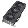
NVIDIA GeForce RTX 4060 Ti 16 GB Review - Twice the VRAM Making a Difference?
Test Setup »High-resolution PCB Pictures
These pictures are for the convenience of volt modders and people who would like to see all the finer details on the PCB. Feel free to link back to us and use these in your articles, videos or forum posts.High-resolution versions are also available (front, back).
Circuit Board (PCB) Analysis
GPU voltage is a six-phase design, managed by a uPI uP9512R controller.
Monolithic Power Systems MP87990 DrMOS components are used for GPU voltage.
Memory voltage is a dual-phase design, managed by a uPI uP1666Q controller.
For memory, Sinopower SM7342EKKP are used.
The memory chips are Samsung K4ZAF325BC-SC20, these are 20 Gbps-rated GDDR6 memory chips. These are the same chips as on the 8 GB version, the only difference is that the 16 GB models have eight memory chips, four on each side.
NVIDIA's AD106 graphics processor is the company's fourth Ada Lovelace GPU. It is built using a 5 nanometer process at TSMC Taiwan, with a transistor count of 22.9 billion and a die size of 190 mm². Please note that the 16 GB version gets its own GPU variant, called AD106-351, whereas the 8 GB version has AD106-350 onboard.
Mar 12th, 2025 22:32 EDT
change timezone
Latest GPU Drivers
New Forum Posts
- What local LLM-s you use? (105)
- Nvidia's GPU market share hits 90% in Q4 2024 (gets closer to full monopoly) (898)
- 22" same price, brand, but not type, compare (0)
- aios... don't leak from the fans.... right? (Fan is acculamating droplets) (13)
- How's your old spinner holding up? (45)
- What else can I do to diagnose an artifacting card? (4)
- Post your Old CDs & FDs, from back in the day thread. (69)
- Zen6 is almost here ? (62)
- I'm looking for a good tool to make the 3D scanning of my mini-pc using the photogrammetry and my Kinect 2. (77)
- Warning message when unlocking PP0 Current Limit (2)
Popular Reviews
- AMD Ryzen 9 9950X3D Review - Great for Gaming and Productivity
- XFX Radeon RX 9070 XT Mercury OC Magnetic Air Review
- Sapphire Radeon RX 9070 XT Nitro+ Review - Beating NVIDIA
- Dough Spectrum Black 32 Review
- ASUS Radeon RX 9070 TUF OC Review
- FSP MP7 Black Review
- AMD Ryzen 7 9800X3D Review - The Best Gaming Processor
- NVIDIA GeForce RTX 5070 Founders Edition Review
- MSI MAG B850 Tomahawk Max Wi-Fi Review
- XPG Starker Air BTF Review
Controversial News Posts
- NVIDIA GeForce RTX 50 Cards Spotted with Missing ROPs, NVIDIA Confirms the Issue, Multiple Vendors Affected (513)
- AMD Radeon RX 9070 and 9070 XT Listed On Amazon - One Buyer Snags a Unit (261)
- AMD RDNA 4 and Radeon RX 9070 Series Unveiled: $549 & $599 (260)
- AMD Mentions Sub-$700 Pricing for Radeon RX 9070 GPU Series, Looks Like NV Minus $50 Again (249)
- NVIDIA Investigates GeForce RTX 50 Series "Blackwell" Black Screen and BSOD Issues (244)
- AMD Radeon RX 9070 and 9070 XT Official Performance Metrics Leaked, +42% 4K Performance Over Radeon RX 7900 GRE (195)
- AMD Radeon RX 9070-series Pricing Leaks Courtesy of MicroCenter (158)
- AMD Radeon RX 9070 XT Reportedly Outperforms RTX 5080 Through Undervolting (101)


