 513
513
NVIDIA GeForce RTX 4060 Ti Founders Edition Review
(513 Comments) »Introduction
NVIDIA today introduces their GeForce RTX 4060 Ti graphics card and we're reviewing the company's in-house GeForce RTX 4060 Ti Founders Edition. The new RTX 4060 Ti is part of a series consisting of the RTX 4060 Ti we're reviewing today, and its 16 GB memory variant that comes out in July, alongside the RTX 4060 non-Ti. All three are designed to plow through the latest games at 1080p resolution, with fairly high settings. NVIDIA stops short of saying that you can max out your game with this card and its 8 GB memory, though we'll find out if you really need double the memory in July, with the 16 GB model.

The GeForce RTX 4060 Ti is based on the same Ada Lovelace graphics architecture as the rest of the RTX 40-series that NVIDIA has been rolling out in a systematic top-down manner, beginning with the enthusiast segment (RTX 4090 and RTX 4080), coming down to the performance segment (RTX 4070 Ti and RTX 4070), and now the mid-range, with the RTX 4060 Ti, RTX 4060 Ti 16 GB, and the RTX 4060.
The new GeForce Ada Lovelace graphics architecture debuts the third generation of RTX, NVIDIA's ground-breaking invention in the consumer graphics space, which combines certain real-time ray traced elements with conventional raster 3D graphics, to significantly improve visual realism. These include ray traced lighting, reflections, shadows, global-illumination, and motion-blur. Even this bit of ray tracing requires enormous compute power, and so NVIDIA has developed fixed-function hardware in the form of RT cores, which it has been generationally enhancing in performance and capabilities.
The GeForce RTX 4060 Ti debuts the new 5 nm AD106 silicon to the desktop space. This chip already powers the mobile RTX 4070 in its maxed out form. The desktop RTX 4060 Ti stops a touch short of doing so, and uses 34 out of 36 streaming multiprocessors (SM) physically present on the silicon, which work out to 4,352 CUDA cores, 34 RT cores, 136 Tensor cores, 48 ROPs, and 136 TMUs. The most fascinating aspect about the RTX 4060 Ti is its memory—you get the same 8 GB as the previous-generation RTX 3060 Ti, but across a generationally narrower memory bus width of 128-bit. We'll provide NVIDIA's explanation about why this shouldn't alarm you, in the Architecture page.
The NVIDIA GeForce RTX 4060 Ti Founders Edition retains the dual-axial flow-through design of Founders Edition graphics cards for the past couple of generations now. Fresh air is drawn in from one of the card's two fans, guided through an intricate set of heatsinks, and exhausted by the second fan. The Founders Edition card retains the modern 16-pin ATX 12VHPWR power connector, which should simplify power connections with modern PSUs. For the rest, the company includes a power adapter that converts two 8-pin PCIe connectors to one of these.
The defining feature of GeForce RTX 4060 Ti, which should sweeten the deal for you compared to buying a previous-generation graphics card, has to be DLSS 3 Frame Generation. Ada GPUs have the ability to leverage the new Optical Flow Accelerator component and its AI-acceleration capabilities, to generate entire alternate frames entirely using AI, and without involving the graphics rendering machinery. This should, in theory, double the frame-rates in games that take advantage of the feature.
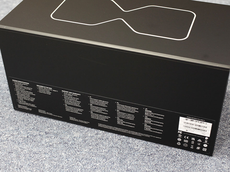
NVIDIA is pricing the GeForce RTX 4060 Ti at an MSRP of USD $399, which is the same exact launch price as its predecessor, the RTX 3060 Ti. The company is encouraging its custom-design board partners to have products at the $399 MSRP, by giving those cards a earlier review NDA of today (May 23). Custom-design cards priced above this $399 price will see their reviews go live tomorrow (May 24), when both kinds of RTX 4060 Ti go on sale.
Short 5-Minute Summary of this Review
Our goal with the videos is to create short summaries, not go into all the details and test results, which can be found on the following pages of this review.
| Price | Cores | ROPs | Core Clock | Boost Clock | Memory Clock | GPU | Transistors | Memory | |
|---|---|---|---|---|---|---|---|---|---|
| RTX 2060 | $180 | 1920 | 48 | 1365 MHz | 1680 MHz | 1750 MHz | TU106 | 10800M | 6 GB, GDDR6, 192-bit |
| RX Vega 64 | $320 | 4096 | 64 | 1247 MHz | 1546 MHz | 953 MHz | Vega 10 | 12500M | 8 GB, HBM2, 2048-bit |
| RX 5700 XT | $180 | 2560 | 64 | 1605 MHz | 1755 MHz | 1750 MHz | Navi 10 | 10300M | 8 GB, GDDR6, 256-bit |
| RTX 3050 | $260 | 2560 | 32 | 1552 MHz | 1777 MHz | 1750 MHz | GA106 | 12000M | 8 GB, GDDR6, 128-bit |
| RTX 2070 | $230 | 2304 | 64 | 1410 MHz | 1620 MHz | 1750 MHz | TU106 | 10800M | 8 GB, GDDR6, 256-bit |
| RX 6600 | $210 | 1792 | 64 | 2044 MHz | 2491 MHz | 1750 MHz | Navi 23 | 11060M | 8 GB, GDDR6, 128-bit |
| RTX 3060 | $300 | 3584 | 48 | 1320 MHz | 1777 MHz | 1875 MHz | GA106 | 12000M | 12 GB, GDDR6, 192-bit |
| RTX 4060 | $300 | 3072 | 32 | 1830 MHz | 2460 MHz | 2125 MHz | AD107 | unknown | 8 GB, GDDR6, 128-bit |
| RX 6600 XT | $250 | 2048 | 64 | 2359 MHz | 2589 MHz | 2000 MHz | Navi 23 | 11060M | 8 GB, GDDR6, 128-bit |
| Arc A750 | $250 | 3584 | 112 | 2050 MHz | N/A | 2000 MHz | ACM-G10 | 21700M | 8 GB, GDDR6, 256-bit |
| Arc A770 | $290 | 4096 | 128 | 2100 MHz | N/A | 2187 MHz | ACM-G10 | 21700M | 16 GB, GDDR6, 256-bit |
| RTX 2080 | $260 | 2944 | 64 | 1515 MHz | 1710 MHz | 1750 MHz | TU104 | 13600M | 8 GB, GDDR6, 256-bit |
| RTX 3060 Ti | $320 | 4864 | 80 | 1410 MHz | 1665 MHz | 1750 MHz | GA104 | 17400M | 8 GB, GDDR6, 256-bit |
| RTX 4060 Ti | $400 | 4352 | 48 | 2310 MHz | 2535 MHz | 2250 MHz | AD106 | 22900M | 8 GB, GDDR6, 128-bit |
| RX 6700 XT | $320 | 2560 | 64 | 2424 MHz | 2581 MHz | 2000 MHz | Navi 22 | 17200M | 12 GB, GDDR6, 192-bit |
| RTX 2080 Ti | $400 | 4352 | 88 | 1350 MHz | 1545 MHz | 1750 MHz | TU102 | 18600M | 11 GB, GDDR6, 352-bit |
| RTX 3070 | $350 | 5888 | 96 | 1500 MHz | 1725 MHz | 1750 MHz | GA104 | 17400M | 8 GB, GDDR6, 256-bit |
| RTX 3070 Ti | $420 | 6144 | 96 | 1575 MHz | 1770 MHz | 1188 MHz | GA104 | 17400M | 8 GB, GDDR6X, 256-bit |
Architecture
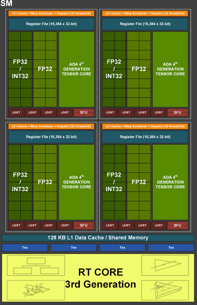
The Ada graphics architecture heralds the third generation of the NVIDIA RTX technology, an effort toward increasing the realism of game visuals by leveraging real-time ray tracing, without the enormous amount of compute power required to draw purely ray-traced 3D graphics. This is done by blending conventional raster graphics with ray traced elements such as reflections, lighting, and global illumination, to name a few. The 3rd generation of RTX introduces the new higher IPC "Ada" CUDA core, 3rd generation RT core, 4th generation Tensor core, and the new Optical Flow Processor, a component that plays a key role in generating new frames without involving the GPU's main graphics rendering pipeline.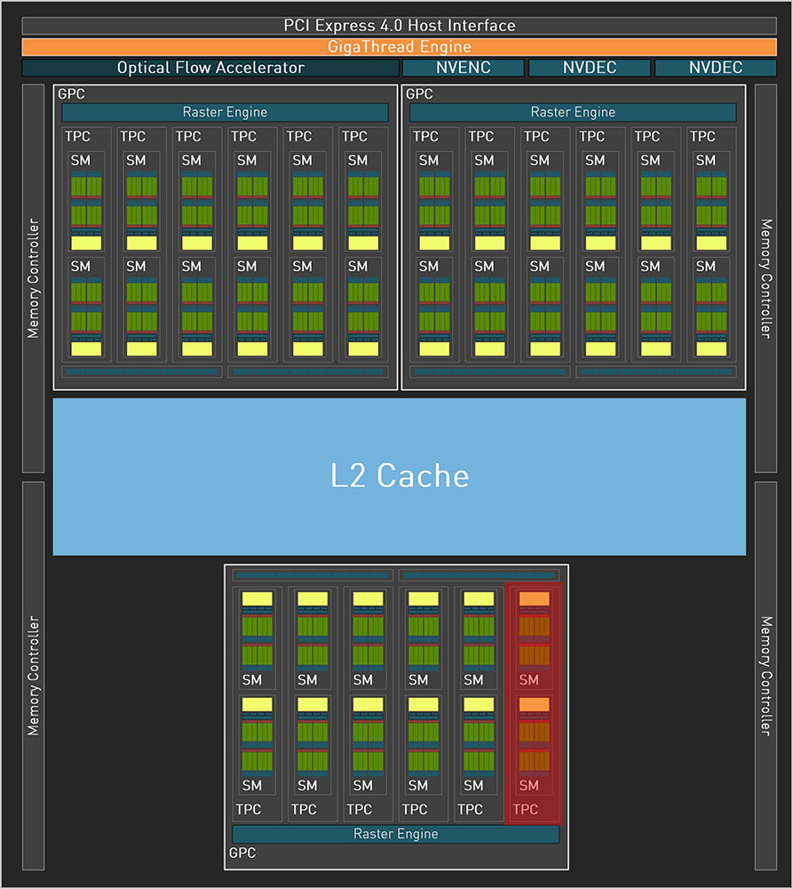
The GeForce Ada graphics architecture driving the RTX 4060 Ti leverages the TSMC 5 nm EUV foundry process to increase transistor counts. At the heart of this GPU is the new AD106 silicon, with a fairly high transistor count of 22.9 billion, which is almost double that of the previous-generation GA106, and still about 30% more than the GA104. The GPU features a generationally narrower PCI-Express 4.0 x8 host interface, and a 128-bit wide GDDR6 memory interface. This is causing some controversy, and we'll present NVIDIA's explanation below. The Optical Flow Accelerator (OFA) is an independent top-level component. The chip features one NVENC and one NVDEC unit.
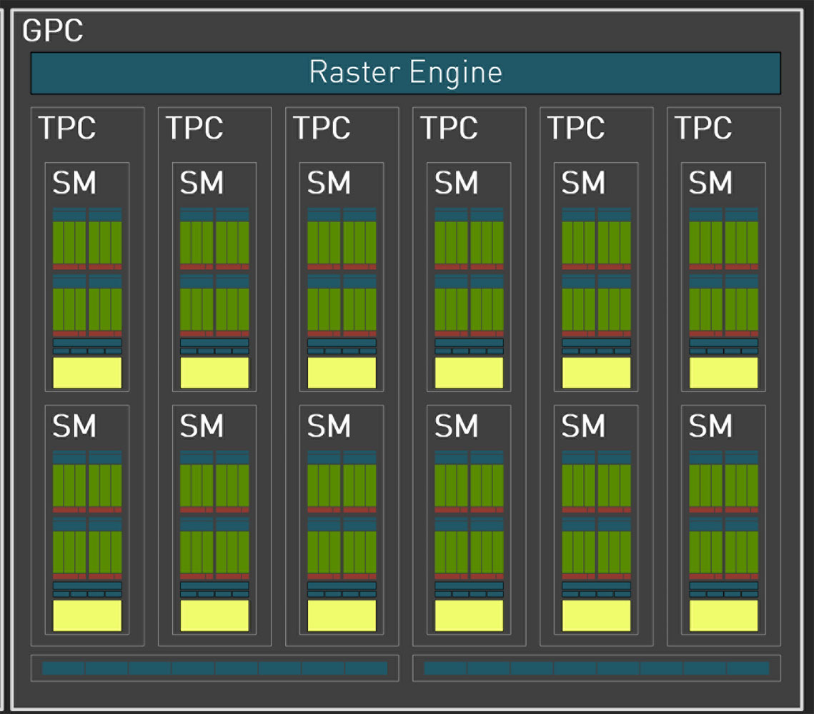
The essential component hierarchy is similar to past generations of NVIDIA GPUs. The AD106 silicon features 3 Graphics Processing Clusters (GPCs), each of these has all the SIMD and graphics rendering machinery, and is a small GPU in its own right. Each GPC shares a raster engine (geometry processing components) and two ROP partitions (each with eight ROP units). The GPC of the AD106 contains five Texture Processing Clusters (TPCs), the main number-crunching machinery. Each of these has two Streaming Multiprocessors (SM), and a Polymorph unit. Each SM contains 128 CUDA cores across four partitions. Half of these CUDA cores are pure-FP32; while the other half is capable of FP32 or INT32. The SM retains concurrent FP32+INT32 math processing capability. The SM also contains a 3rd generation RT core, four 4th generation Tensor cores, some cache memory, and four TMUs. There are 12 SM per GPC, so 1,536 CUDA cores, 48 Tensor cores, and 12 RT cores; per GPC. There are three such GPCs, which add up to 4,608 CUDA cores, 144 TMUs, 144 Tensor Cores, and 36 RT cores. Each GPC contributes 16 ROPs, so there are 48 ROPs on the silicon. The RTX 4060 Ti is carved out of the AD106 by disabling one TPC worth 256 CUDA cores. This yields 4,352 CUDA cores, 136 Tensor cores, 34 RT cores, and 136 TMUs. The ROP count is untouched at 48, as is the on-die L2 cache sees a slight reduction, which is 32 MB in size.
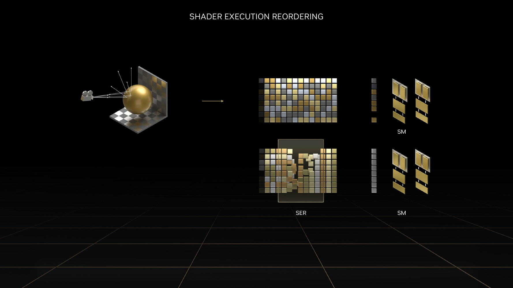
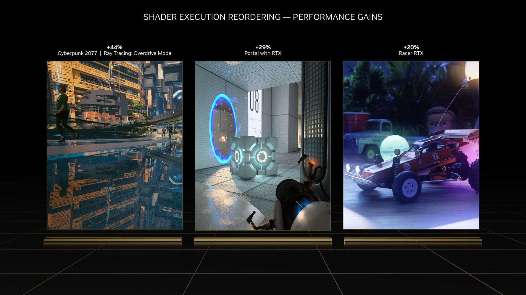
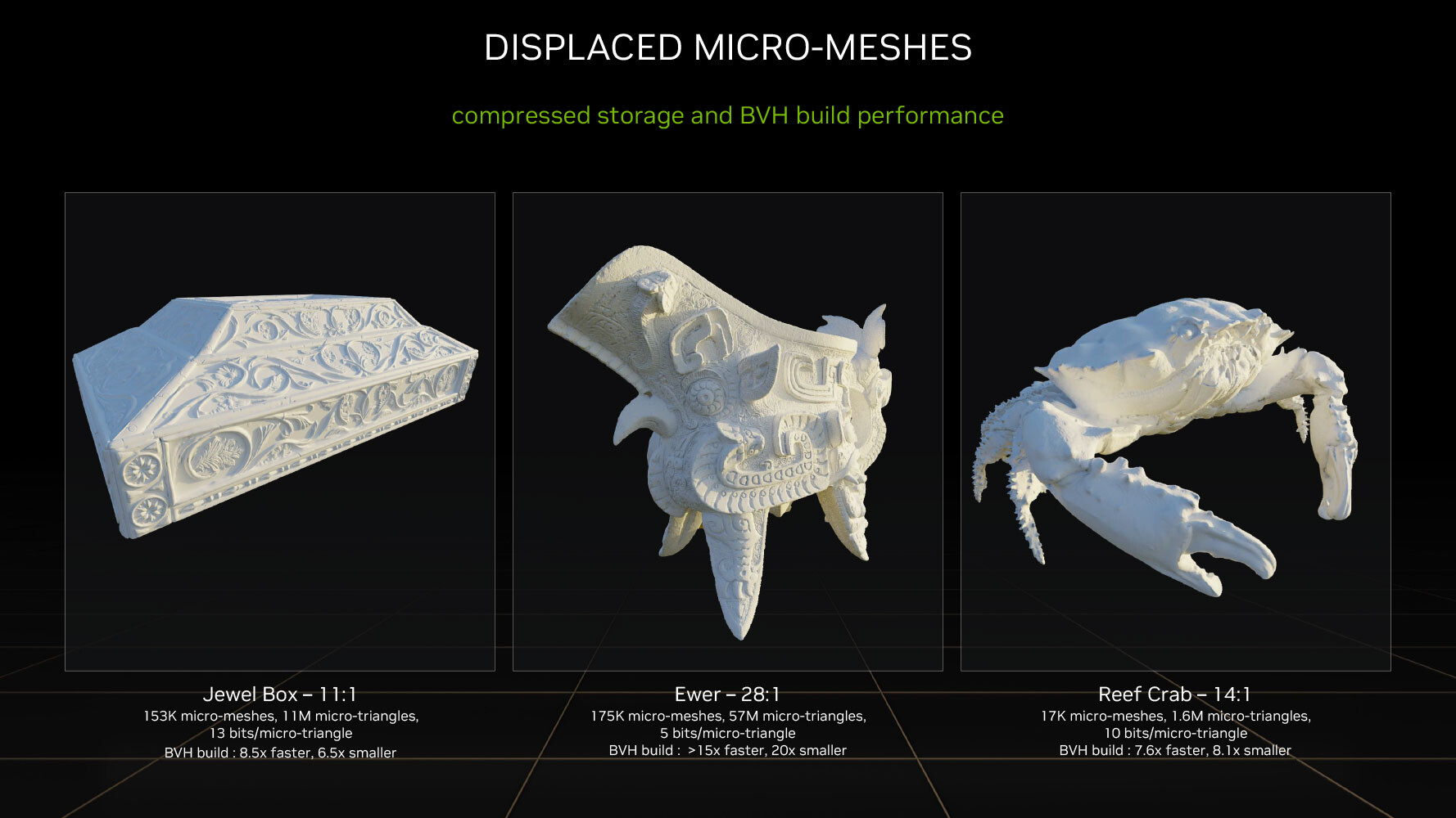
The 3rd generation RT core accelerates the most math-intensive aspects of real-time ray tracing, including BVH traversal. Displaced micro-mesh engine is a revolutionary feature introduced with the new 3rd generation RT core. Just as mesh shaders and tessellation have had a profound impact on improving performance with complex raster geometry, allowing game developers to significantly increase geometric complexity; DMMs is a method to reduce the complexity of the bounding-volume hierarchy (BVH) data-structure, which is used to determine where a ray hits geometry. Previously, the BVH had to capture even the smallest details to properly determine the intersection point. Ada's ray tracing architecture also receives a major performance uplift from Shader Execution Reordering (SER), a software-defined feature that requires awareness from game-engines, to help the GPU reorganize and optimize worker threads associated with ray tracing.
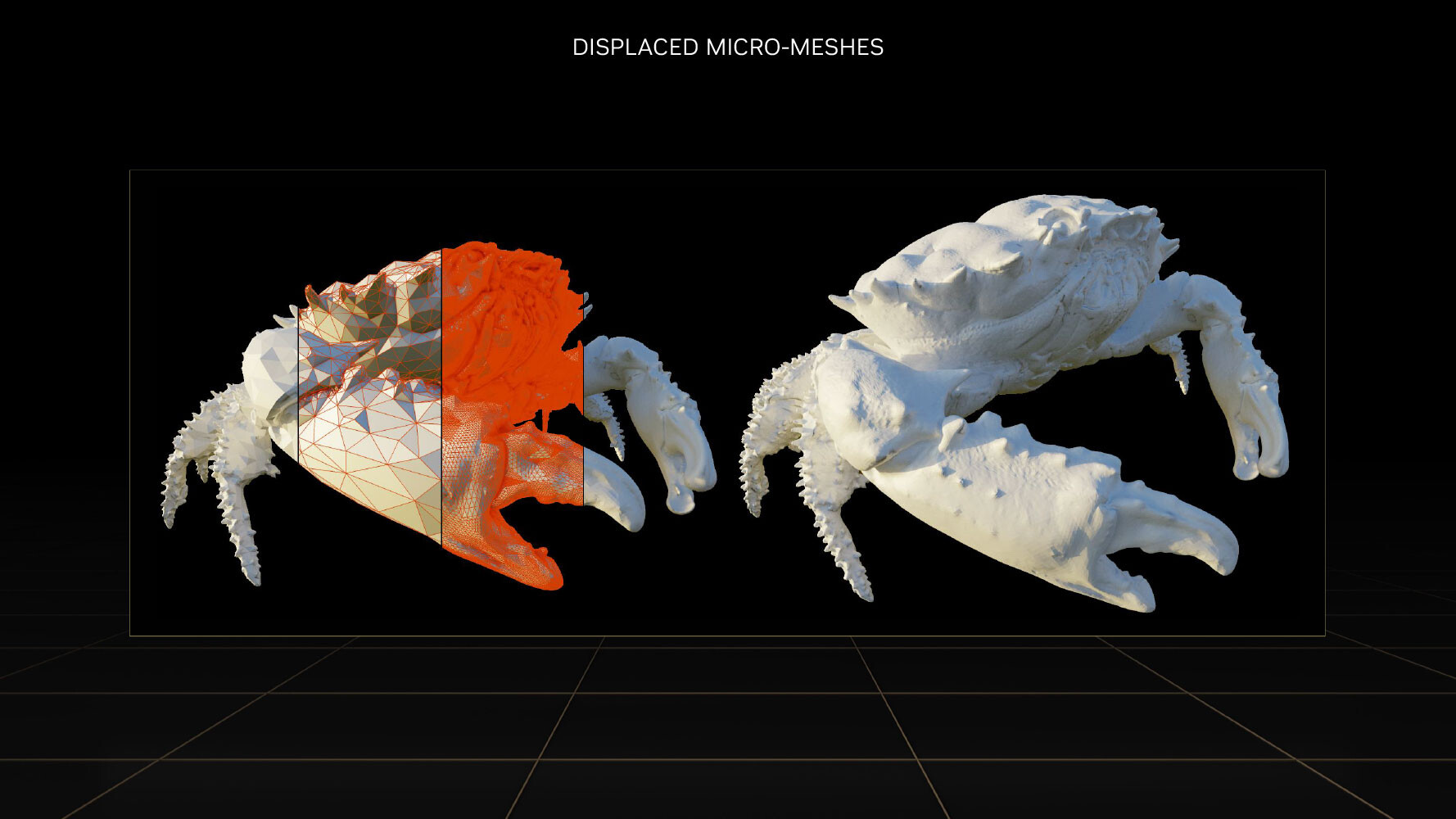
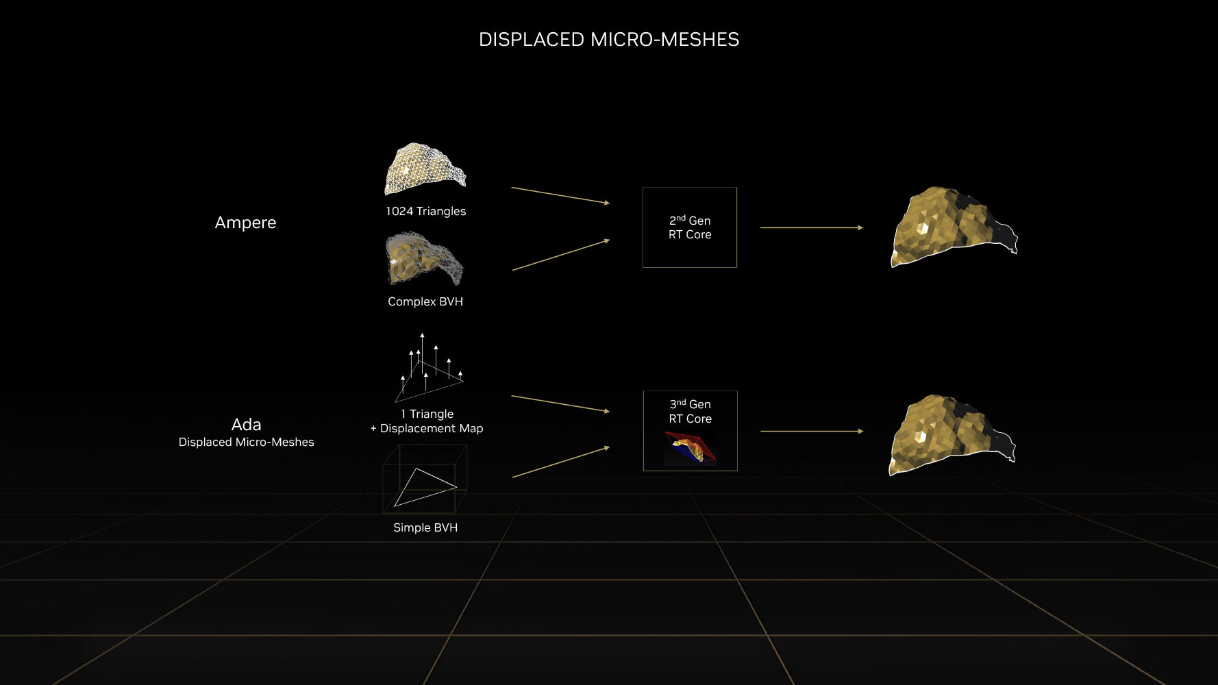
The BVH now needn't have data for every single triangle on an object, but can represent objects with complex geometry as a coarse mesh of base triangles, which greatly simplifies the BVH data structure. A simpler BVH means less memory consumed and helps to greatly reduce ray tracing CPU load, because the CPU only has to generate a smaller structure. With older "Ampere" and "Turing" RT cores, each triangle on an object had to be sampled at high overhead, so the RT core could precisely calculate ray intersection for each triangle. With Ada, the simpler BVH, plus the displacement maps can be sent to the RT core, which is now able to figure out the exact hit point on its own. NVIDIA has seen 11:1 to 28:1 compression in total triangle counts. This reduces BVH compile times by 7.6x to over 15x, in comparison to the older RT core; and reducing its storage footprint by anywhere between 6.5 to 20 times. DMMs could reduce disk- and memory bandwidth utilization, utilization of the PCIe bus, as well as reduce CPU utilization. NVIDIA worked with Simplygon and Adobe to add DMM support for their tool chains.
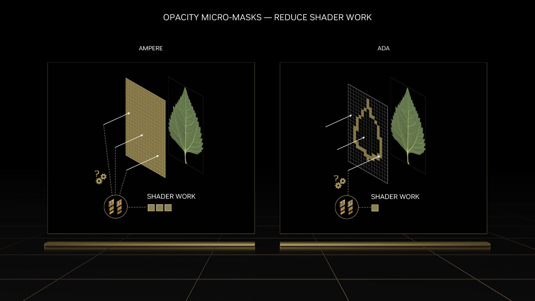
Opacity Micro Meshes (OMM) is a new feature introduced with Ada to improve rasterization performance, particularly with objects that have alpha (transparency data). Most low-priority objects in a 3D scene, such as leaves on a tree, are essentially rectangles with textures on the leaves where the transparency (alpha) creates the shape of the leaf. RT cores have a hard time intersecting rays with such objects, because they're not really in the shape that they appear (they're really just rectangles with textures that give you the illusion of shape). Previous-generation RT cores had to have multiple interactions with the rendering stage to figure out the shape of a transparent object, because they couldn't test for alpha by themselves.
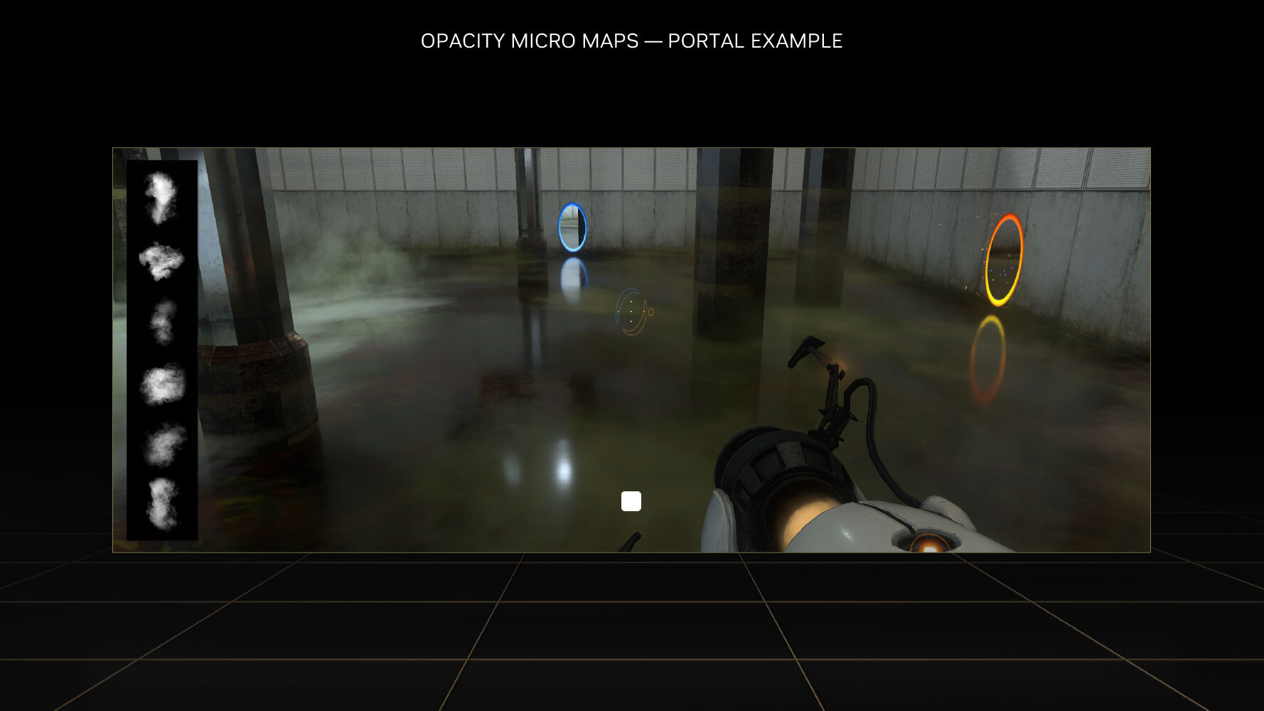
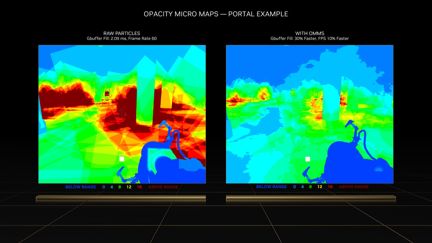
This has been solved by using OMMs. Just as DMMs simplify geometry by creating meshes of micro-triangles; OMMs create meshes of rectangular textures that align with parts of the texture that aren't alpha, so the RT core has a better understanding of the geometry of the object, and can correctly calculate ray intersections. This has a significant performance impact on shading performance in non-RT applications, too. Practical applications of OMMs aren't just low-priority objects such as vegetation, but also smoke-sprites and localized fog. Traditionally there was a lot of overdraw for such effects, because they layered multiple textures on top of each other, that all had to be fully processed by the shaders. Now only the non-opaque pixels get executed—OMMs provide a 30 percent speedup with graphics buffer fill-rates, and a 10 percent impact on frame-rates.
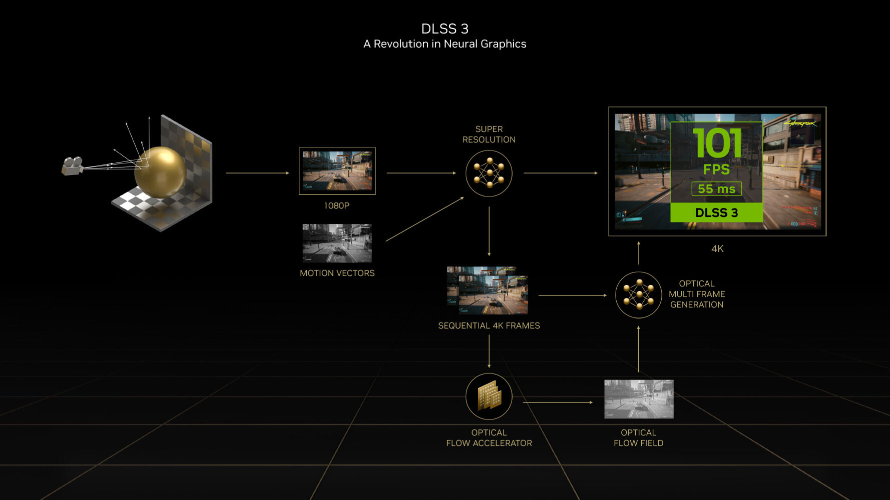
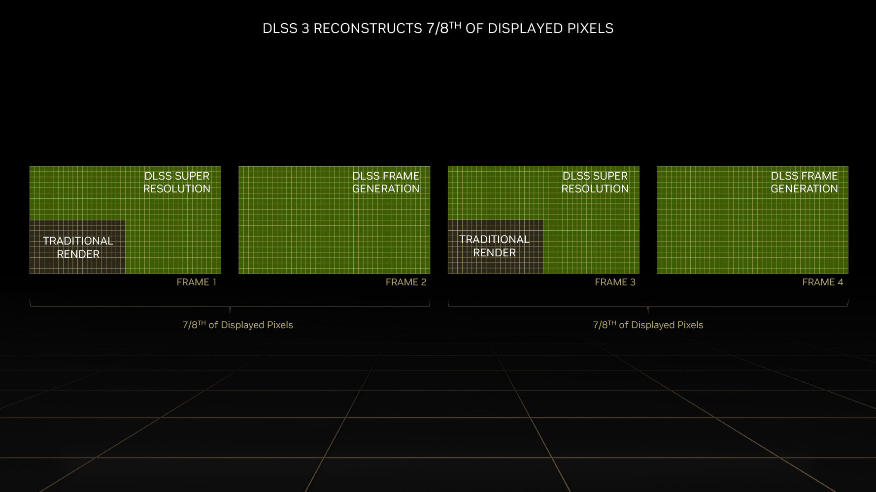
DLSS 3 introduces a revolutionary new feature that promises a doubling in frame-rate at comparable quality, it's called AI frame-generation. While it has all the features of DLSS 2 and its AI super-resolution (scaling up a lower-resolution frame to native resolution with minimal quality loss); DLSS 3 can generate entire frames simply using AI, without involving the graphics rendering pipeline. Later in the article, we will show you DLSS 3 in action.
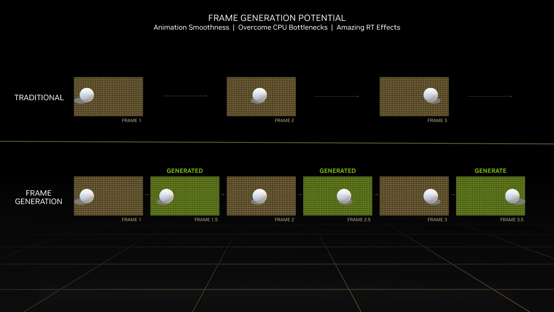
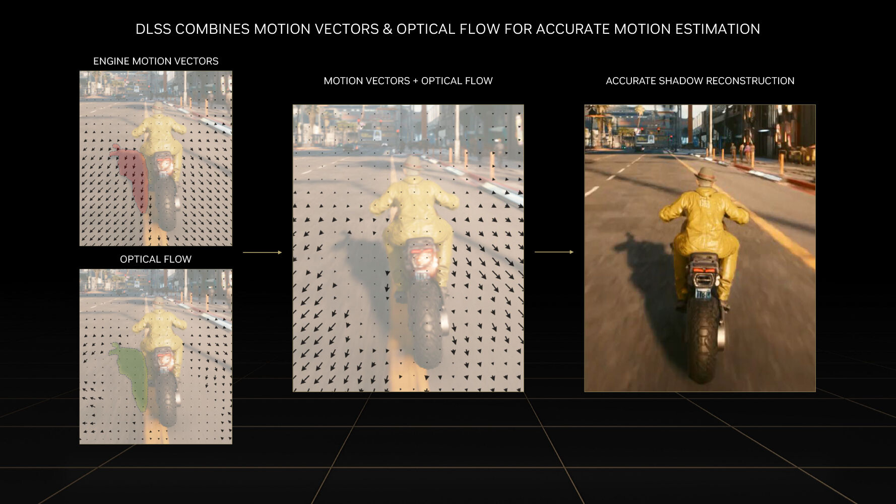
Every alternating frame with DLSS 3 is hence AI-generated, without being a replica of the previous rendered frame. This is possible only on the Ada graphics architecture, because of a hardware component called the optical flow accelerator (OFA), which assists in predicting what the next frame could look like, by creating what NVIDIA calls an optical flow-field. OFA ensures that the DLSS 3 algorithm isn't confused by static objects in a rapidly-changing 3D scene (such as a race sim). The process heavily relies on the performance uplift introduced by the FP8 math format of the 4th generation Tensor core. A third key ingredient of DLSS 3 is Reflex. By reducing the rendering queue to zero, Reflex plays a vital role in ensuring that frame-times with DLSS 3 are at an acceptable level, and a render-queue doesn't confuse the upscaler. A combination of OFA and the 4th Gen Tensor core is why the Ada architecture is required to use DLSS 3, and why it won't work on older architectures.
Ada Rebalanced Memory Subsystem
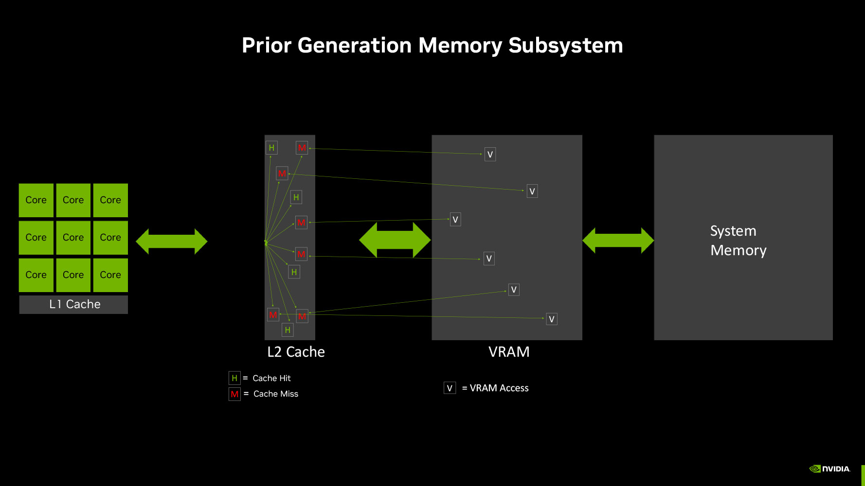
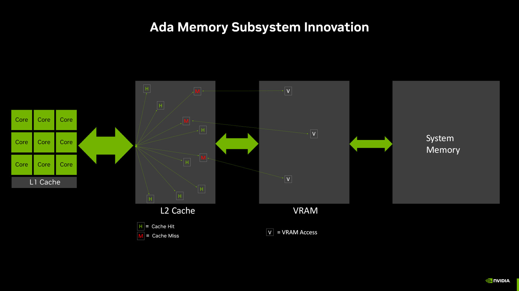
The previous-generation GeForce RTX 3060 Ti featured a 256-bit wide GDDR6 memory interface driving its 8 GB of 14 Gbps-rated GDDR6 memory (448 GB/s memory bandwidth), which has caused some controversy with the new RTX 4060 Ti using a narrower 128-bit wide memory interface to drive 8 GB of 18 Gbps memory (288 GB/s bandwidth). With the new Ada Lovelace graphics architecture, NVIDIA has tried to re-balance the memory sub-system such that there's dependence on larger on-die caches, allowing NVIDIA to narrow down the GPU's GDDR6 memory interface. The obvious benefit of this to NVIDIA is reduced costs, let's make no mistake about it, but NVIDIA maintains that this isn't a big problem for the GPU.
The last-level cache, or L2 cache, of NVIDIA Ada GPUs is anywhere between 8-10 times larger than the ones on the previous-generation Ampere GPUs. The AD106 silicon powering the RTX 4060 Ti has a 32 MB L2 cache, compared to the 4 MB of the GA104 silicon powering the RTX 3060 Ti. NVIDIA illustrated an example of how a the larger on-die LLC reduces video memory pressure (trips to GDDR6) by anywhere between 40% to 60% on the same GPU, by soaking up a larger number of memory access requests by the shaders.
The L2 cache is unified victim cache to the GPU's various GPCs and their local TPCs. Data that isn't hot enough (frequently accessed enough) to be resident on the small L1 caches of the SM, is ejected to the L2 cache, and depending on its heat, pushed to the GDDR6 video memory. The L2 cache is an order of magnitude faster than than video memory in terms of latency, and so having frequently-accessed data reside there offers a considerable benefit.
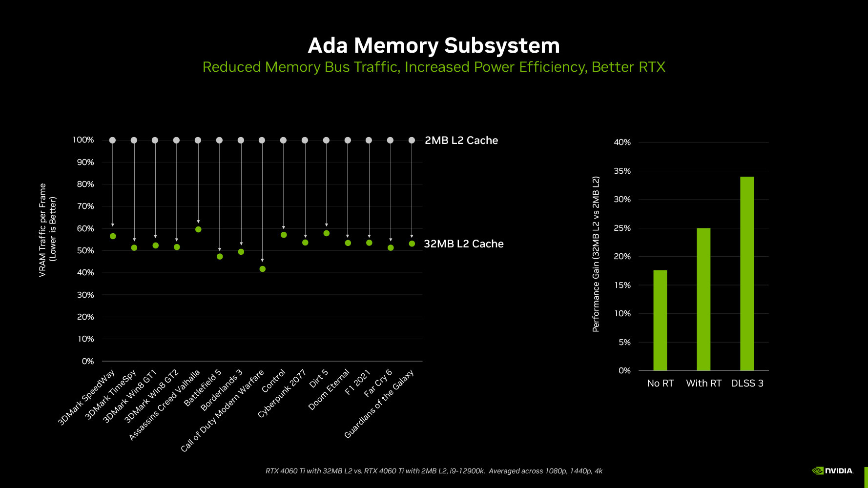
As we mentioned earlier from NVIDIA's claims, this re-balancing of the memory sub-system between the on-die LLC and video memory lowers the GPU's access to the latter by as much as 60%, which means the GPU can make do with a narrower 128-bit wide GDDR6 memory bus. NVIDIA has used generationally faster 18 Gbps memory chips in the RTX 4060 Ti. NVIDIA developed a new means of presenting the memory bandwidth that takes into account the contribution of the L2 cache, its hit-rate, and the consequent reduction in video memory traffic. While the memory bandwidth of the RTX 4060 Ti is 288 GB/s, NVIDIA claims that its "effective bandwidth" is 554 GB/s (23% higher than the 448 GB/s memory bandwidth of the RTX 3060 Ti). It's interesting to point out that NVIDIA has used "effective bandwidth" figures in the past to highlight its lossless memory compression technologies, but has never been this vocal about it.
Packaging
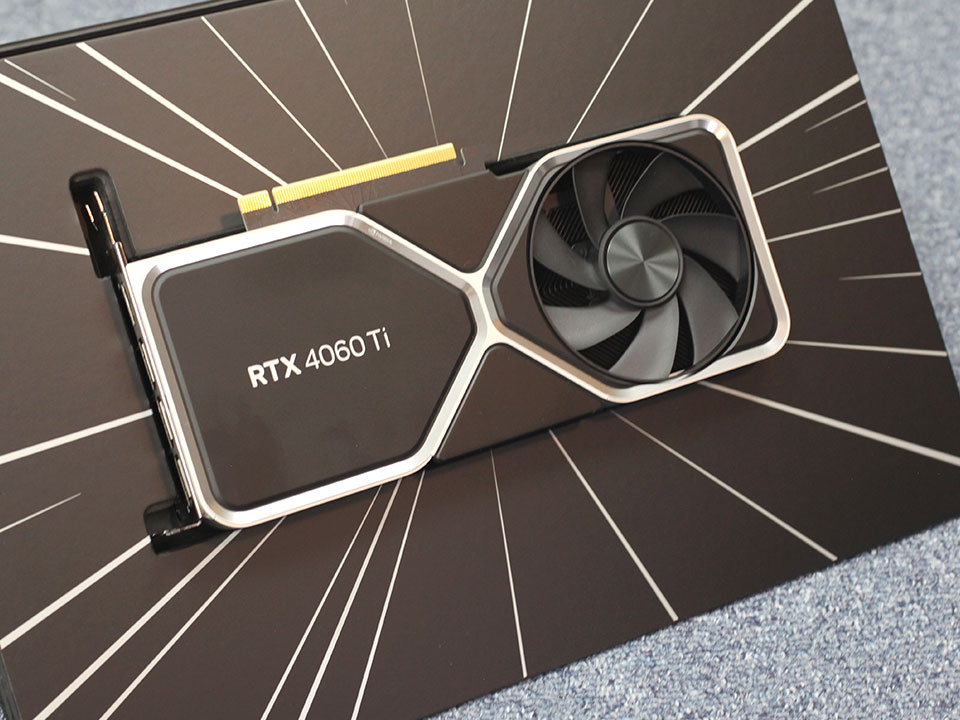
The Card
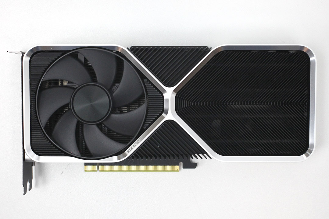
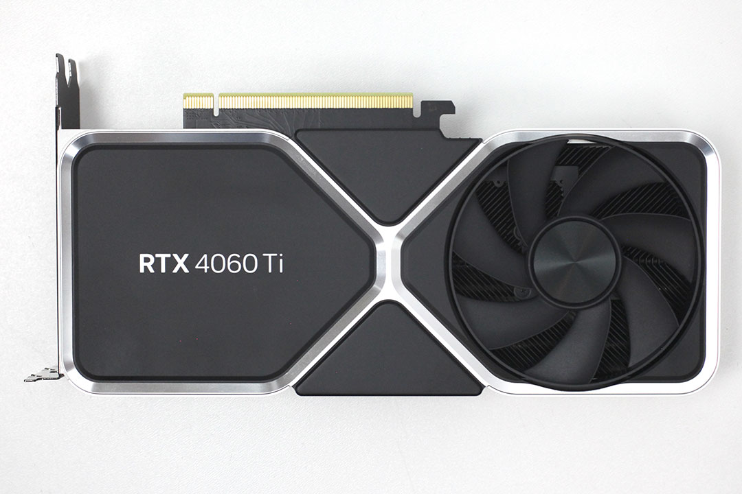
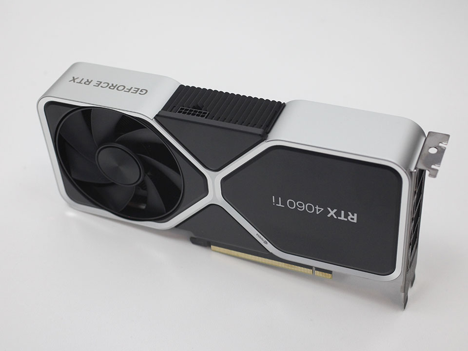
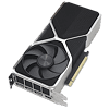
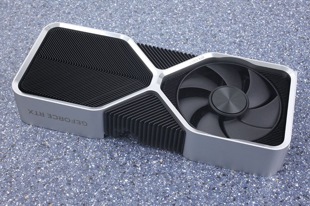
NVIDIA's Founders Edition looks stunning—it could be an Apple product. Compared to the GeForce 30 Series, NVIDIA has made small improvements to the design language, making it an even cleaner design than before. As with Ampere, the card is designed for airflow to go through the card—that's why there's two fans. One sucks in cool air from the bottom, is pushed through the card and then blown out towards the case top on the other side. Compared to the other GeForce 40 Founders Editions there's subtle color differences, but nothing major.
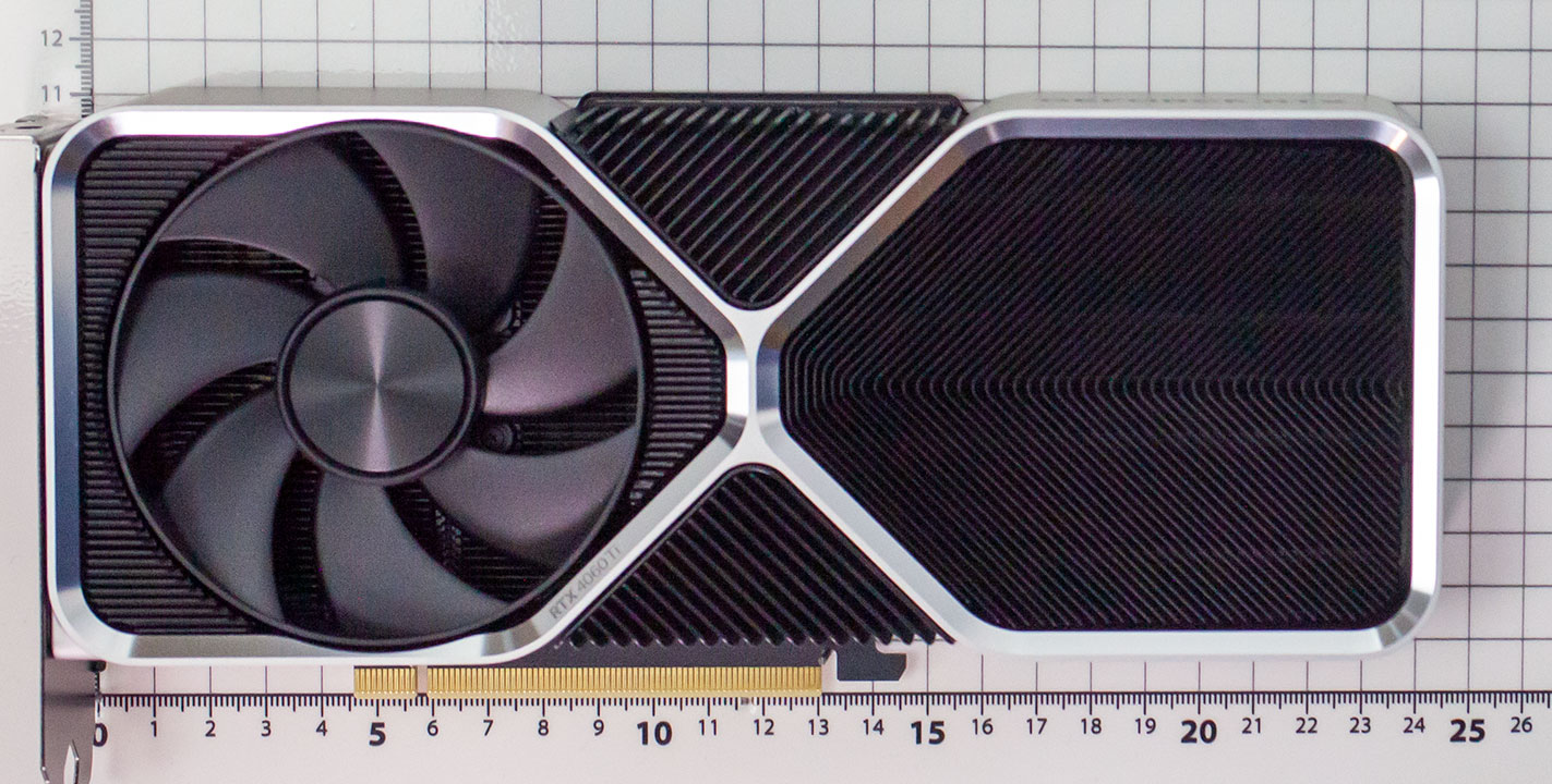
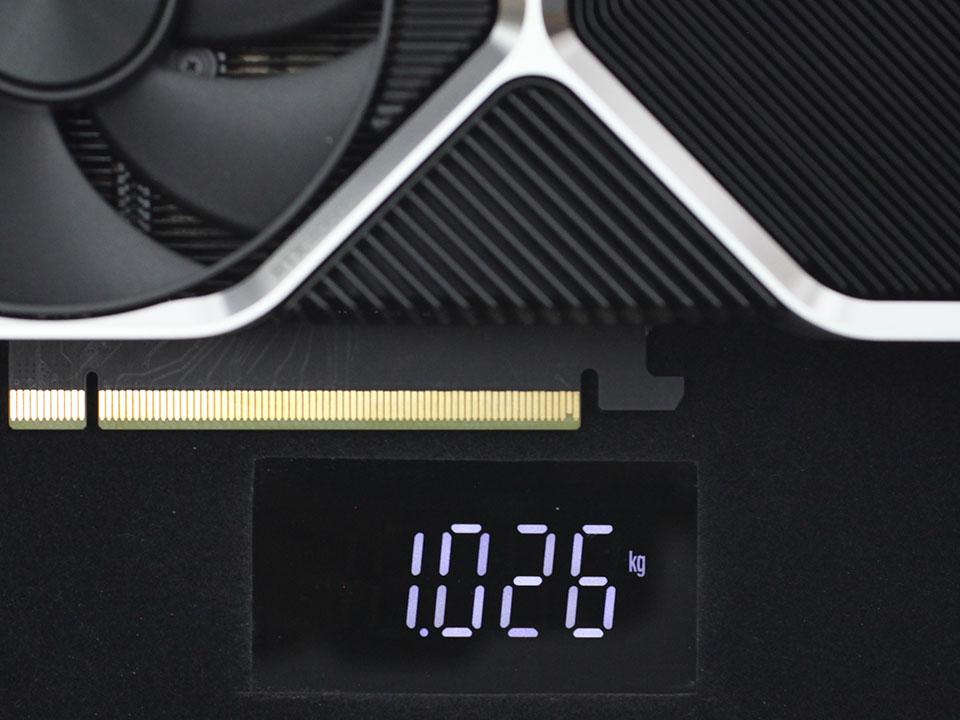
Dimensions of the card are 25.0 x 11.0 cm, and it weighs 1026 g.
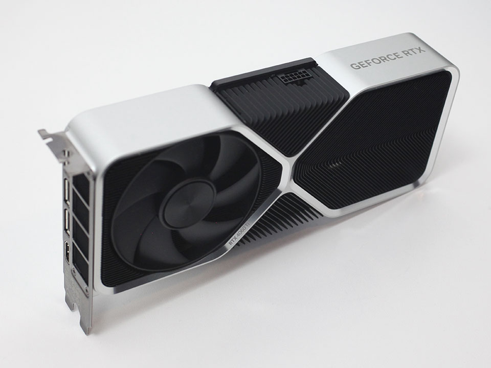
Installation requires two slots in your system.
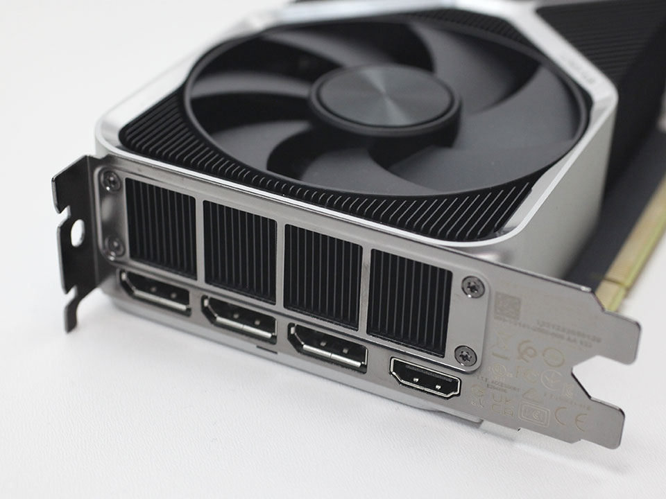
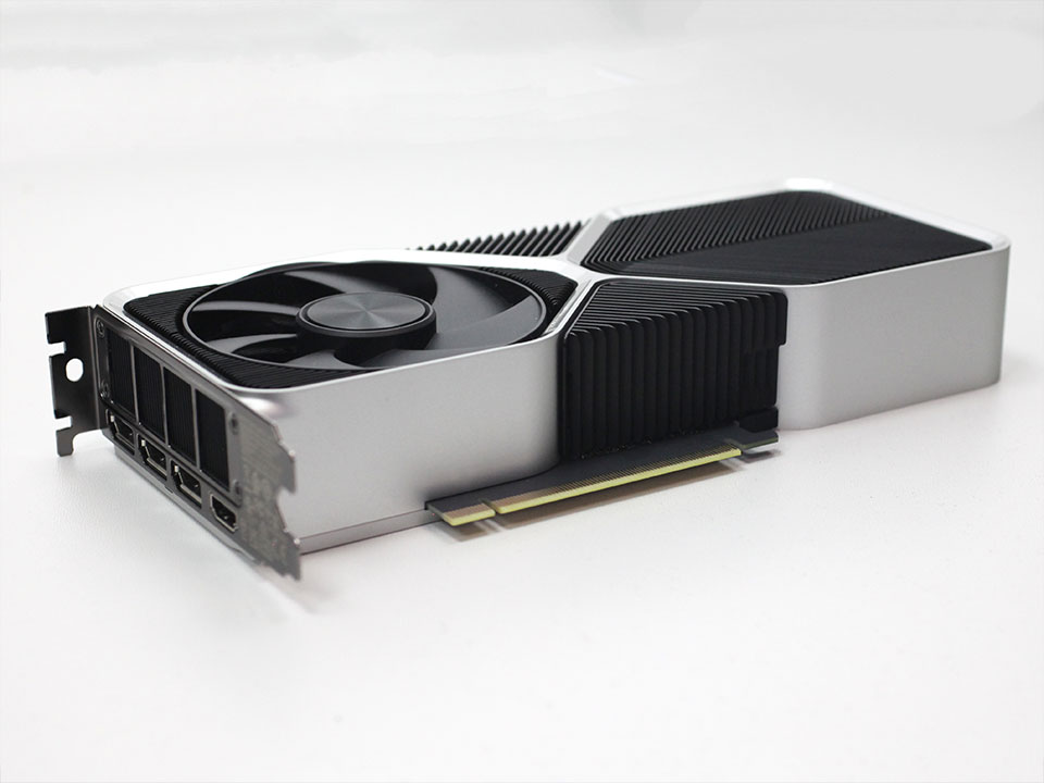
Display connectivity includes three standard DisplayPort 1.4a ports and one HDMI 2.1a (same as Ampere).
NVIDIA introduced the concept of dual NVDEC and NVENC Codecs with the Ada Lovelace architecture. This means there are two independent sets of hardware-accelerators; so you can encode and decode two streams of video in parallel or one stream at double the FPS rate. The new 8th Gen NVENC now accelerates AV1 encoding, besides HEVC. You also get an "optical flow accelerator" unit that is able to calculate intermediate frames for videos, to smooth playback. The same hardware unit is used for frame generation in DLSS 3.
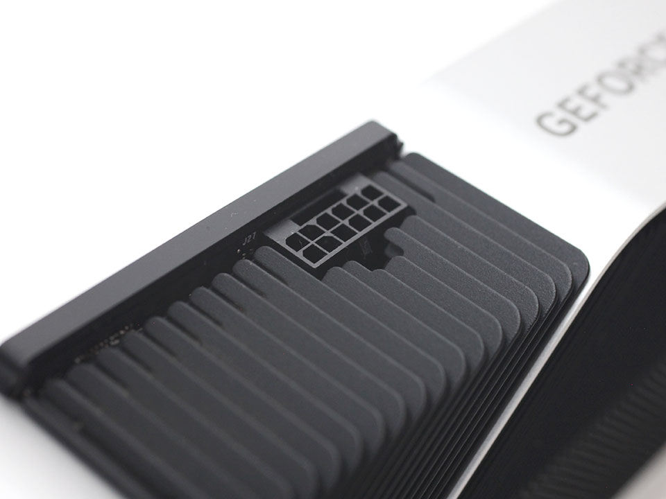
The card uses the new 12+4 pin ATX 12VHPWR connector, which is rated for up to 600 W of power draw. An adapter cable from 1x PCIe 8-pin is included (which is rated for up to 150 W). The card's default power limit is 160 W. Of course the 2x, 3x and 4x 8-pin to 16-pin adapter cables from other Ampere cards will work with the RTX 4070, but the card won't need or use that much power.
Teardown
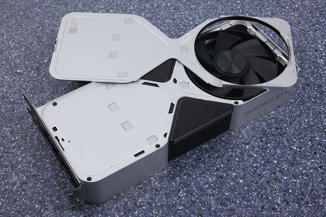
Disassembly is similar to earlier Founders Edition graphics cards. First pop off the top cover, it's attached magnetically—great idea.
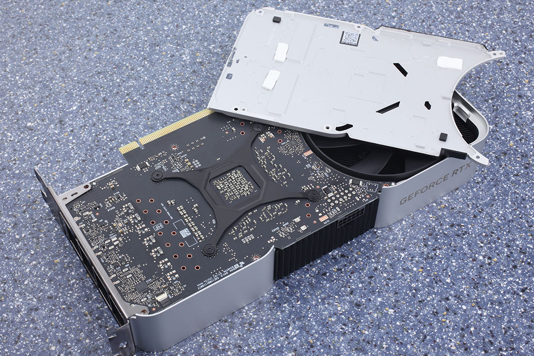
Now remove several Torx screws. With the back cover removed, we have to disconnect two flat-ribbon cables. Use your fingers where possible, instead of metal tools. Flip the connector latch up, as displayed in the second photo, then carefully pull out the cable. Remove the screws on the slot cover and you can remove the heatsink from the PCB.
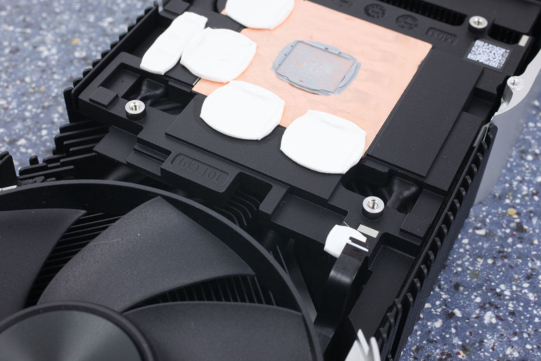
NVIDIA has installed four heatpipes that move heat away from the GPU surface.
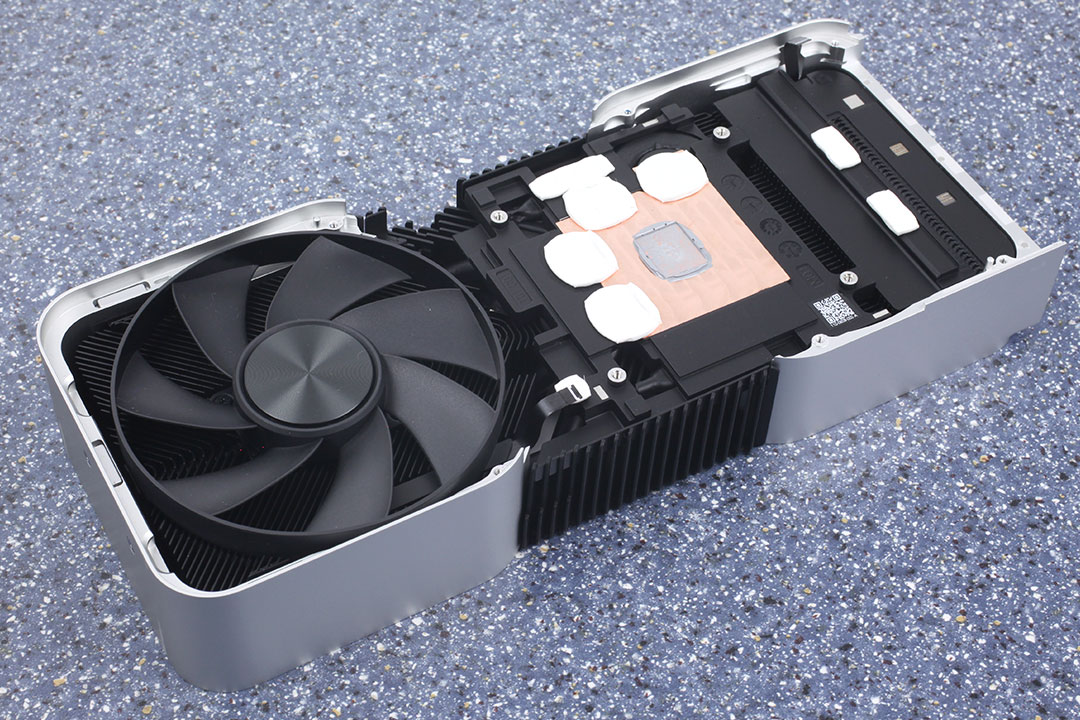
The cooler has a copper base and provides cooling for the memory chips and VRM circuitry, too.
Our Patreon Silver Supporters can read articles in single-page format.
Apr 14th, 2025 20:23 EDT
change timezone
Latest GPU Drivers
New Forum Posts
- New PC case - Other Options to Asus AP201 (1)
- 7800X3D and 5070 Ti / 9070 XT Build (13)
- Flash another RTX 4060 vBIOS to get zero rpm fan support (0)
- The TPU UK Clubhouse (26088)
- What's your latest tech purchase? (23552)
- Share your AIDA 64 cache and memory benchmark here (3052)
- RX 9000 series GPU Owners Club (316)
- Advice on GPU upgrade (51)
- Weird pc slow down as soon as PCI-E card is in the system (5)
- best ram to buy for my usage and system specs? (24)
Popular Reviews
- ASUS GeForce RTX 5080 TUF OC Review
- G.SKILL Trident Z5 NEO RGB DDR5-6000 32 GB CL26 Review - AMD EXPO
- Thermaltake TR100 Review
- The Last Of Us Part 2 Performance Benchmark Review - 30 GPUs Compared
- TerraMaster F8 SSD Plus Review - Compact and quiet
- Zotac GeForce RTX 5070 Ti Amp Extreme Review
- Sapphire Radeon RX 9070 XT Pulse Review
- Sapphire Radeon RX 9070 XT Nitro+ Review - Beating NVIDIA
- Upcoming Hardware Launches 2025 (Updated Apr 2025)
- DAREU A950 Wing Review
Controversial News Posts
- NVIDIA GeForce RTX 5060 Ti 16 GB SKU Likely Launching at $499, According to Supply Chain Leak (182)
- NVIDIA Sends MSRP Numbers to Partners: GeForce RTX 5060 Ti 8 GB at $379, RTX 5060 Ti 16 GB at $429 (124)
- Nintendo Confirms That Switch 2 Joy-Cons Will Not Utilize Hall Effect Stick Technology (105)
- Over 200,000 Sold Radeon RX 9070 and RX 9070 XT GPUs? AMD Says No Number was Given (100)
- Nintendo Switch 2 Launches June 5 at $449.99 with New Hardware and Games (99)
- Sony Increases the PS5 Pricing in EMEA and ANZ by Around 25 Percent (87)
- NVIDIA Pushes GeForce RTX 5060 Ti Launch to Mid-April, RTX 5060 to May (77)
- NVIDIA PhysX and Flow Made Fully Open-Source (77)