 708
708
Sapphire Radeon RX 9070 XT Nitro+ Review - Beating NVIDIA
(708 Comments) »Introduction
AMD's next generation of gaming graphics cards is here to breathe life into a market stiflingly inflated prices, and we have with us the Sapphire Radeon RX 9070 XT NITRO+. The NITRO line of graphics cards represents the very best in graphics card design by Sapphire, one of AMD's oldest and most important board partners, and given that the RX 9070 XT is the top-spec part from the RX 9000 series, the company has thrown everything and the kitchen sink into this product. The Radeon RX 9070 XT is a performance-segment graphics card that AMD claims is capable of 4K Ultra HD gaming. The company goes as far as to claim that this GPU has "everything you need" for that resolution, at a confidence-inspiring starting price of $600, which is slightly above that of the GeForce RTX 5070 that NVIDIA is launching today.

The Radeon RX 9070 XT is powered by RDNA 4, the fourth generation of the RDNA graphics architecture that has seen AMD's return to competitiveness in the gaming GPU market. The RX 5000 series had enough performance to disrupt RTX 20-series Turing, causing it to launch the RTX 20 Super series; the RX 6000 RDNA 2 series was commercially a heyday for AMD, as that's when the crypto mining boom soaked up all premium and enthusiast GPUs, while the products themselves squared off well against NVIDIA's RTX 30-series Ampere. The RX 7000 series powered by RDNA 3 fell sightly behind in competitiveness, and AMD identified a crucial reason—naming.
While the RX 6800 XT performed in the same league as the RTX 3080 and ray tracing performance wasn't a big differentiator, its successor, the RX 7800 XT was significantly slower than the RTX 4080, which wasn't just faster but also priced nearly double that of the AMD card. Meanwhile, gamers began more direct comparisons between AMD and NVIDIA SKUs based on naming, and found that even the RTX 4070 Ti was a faster pick than the RX 7800 XT. AMD had to come up with the RX 7900 GRE, which offered comparable performance at a better priced, but only compounded the problem of naming—you now had an RX 7900 series product compete with an RTX 4070 series. It is to address exactly this, that AMD decided to give its gaming GPU series a significant change with product naming.
The Radeon RX 9070 XT is part of the Radeon 9000 series, and within it, is a xx70-segment product. Its name guides gamers to compare it with the RTX 5070 and the RTX 5070 Ti, although at a starting price of $600, the company aims to offer better performance than the RTX 5070 at better price-performance than the RTX 5070 Ti, which starts at $750. With the RX 9000 series, AMD is withdrawing from the enthusiast segment. It's hard to speculate why, but this means that the company gets to flex its engineering muscle at making the RX 9070 XT at least a segment-best GPU.
The RDNA 4 graphics architecture is purpose built for two things—to pack the most performance per mm² die-area, and to allow AMD to wage price-wars against the RTX 5070 series SKUs. The company claims a significant increase in performance-per-CU over the previous RDNA 3 architecture, with which it can achieve its performance targets using 64 CU spread across 4 shader engines. The company also claims a 100% increase in ray tracing performance over RDNA 3, which should reduce the performance cost of ray tracing. There is a similar leap in AI acceleration throughput, now close to 1600 AI TOPS, paving the way for FSR 4, the biggest upgrade to the FSR suite of performance enhancements. FSR 4 uses a new AI ML-based upscaler that offers superior image quality at every performance preset.
The Radeon RX 9070 XT and RX 9070 that we're also reviewing today, share a common silicon, the 4 nm Navi 48, which the RX 9070 XT maxes out. Unlike NVIDIA, which stuck to the exact same process node for the Blackwell generation as the Ada generation, AMD gave the Navi 48 two key process-level upgrades. Firstly, the company switched to the 4 nm TSMC N4P node, which offers clock speed and efficiency upgrades over the previous TSMC N5 node, and secondly, Navi 48 is a monolithic silicon unlike Navi 32, which was a chiplet-based GPU with a 5 nm GCD and 6 nm MCDs. The entire Navi 48 chip is made on 4 nm, including the memory controllers and Infinity Cache, and then there are power management and IPC improvements from the RDNA 4 architecture.
The Navi 48 silicon features 64 RDNA 4 compute units (CU), all of which are enabled on the RX 9070 XT. This works out to 4,096 stream processors, 128 AI accelerators, 64 RT accelerators, 256 TMUs, and 128 ROPs (an increase over the 96 ROPs than the Navi 32 came with). The card comes with 16 GB of memory across a 256-bit wide memory interface, although what's interesting is that AMD stuck with older GDDR6 memory standard, using 20 Gbps memory speeds, which results in 640 GB/s of memory bandwidth. AMD is counting on new architecture-level features, such as out-of-order memory management, and the 64 MB Infinity Cache, to keep the RX 9070 series competitive with the GeForce RTX 5070 series.
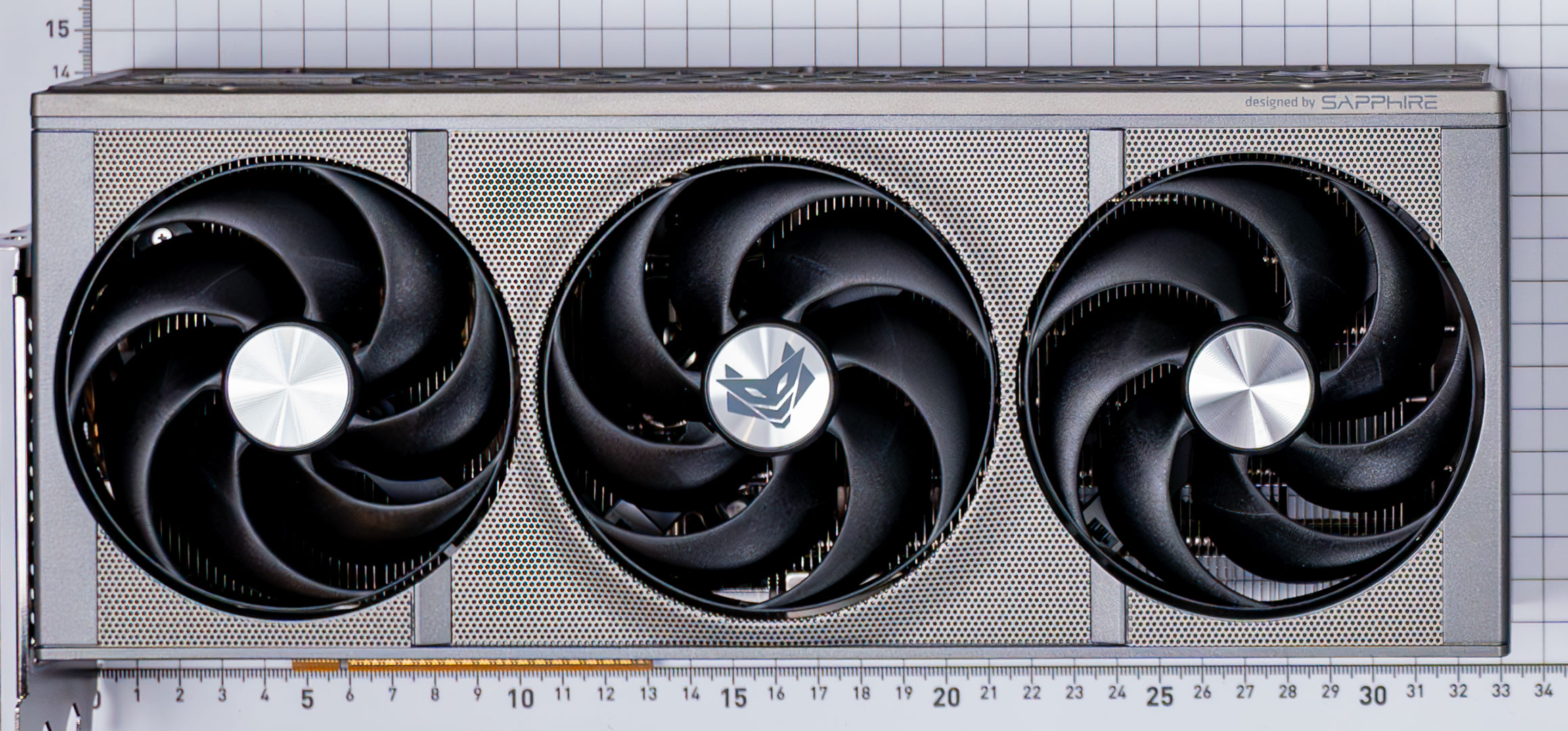
The Sapphire Radeon RX 9070 XT NITRO+ comes with a stunning custom design that looks like it's a piece of jewellery. The triple-slot cooling solution features a dense aluminium fin-stack heatsink, and a premium high-conductivity TIM. This is probably the only premium custom design RX 9070 XT to implement a 16-pin 12V-2x6 power input, which is neatly tucked away, more on this in the picture pages. The NITRO+ also comes with a generous amount of RGB LED lighting in the form of a large RGB diffuser that spans the length of the card. The card comes with factory overclocked speeds of 2520 MHz Game clock, a generous increase over the 2400 MHz reference. Sapphire is pricing the Radeon RX 9070 XT NITRO+ at $730, a $130 premium over the $600 starting price for the RX 9070 XT.
| Price | Cores | ROPs | Core Clock | Boost Clock | Memory Clock | GPU | Transistors | Memory | |
|---|---|---|---|---|---|---|---|---|---|
| RTX 3080 | $420 | 8704 | 96 | 1440 MHz | 1710 MHz | 1188 MHz | GA102 | 28000M | 10 GB, GDDR6X, 320-bit |
| RTX 4070 | $490 | 5888 | 64 | 1920 MHz | 2475 MHz | 1313 MHz | AD104 | 35800M | 12 GB, GDDR6X, 192-bit |
| RX 7800 XT | $440 | 3840 | 96 | 2124 MHz | 2430 MHz | 2425 MHz | Navi 32 | 28100M | 16 GB, GDDR6, 256-bit |
| RX 6900 XT | $450 | 5120 | 128 | 2015 MHz | 2250 MHz | 2000 MHz | Navi 21 | 26800M | 16 GB, GDDR6, 256-bit |
| RX 6950 XT | $630 | 5120 | 128 | 2100 MHz | 2310 MHz | 2250 MHz | Navi 21 | 26800M | 16 GB, GDDR6, 256-bit |
| RTX 3090 | $900 | 10496 | 112 | 1395 MHz | 1695 MHz | 1219 MHz | GA102 | 28000M | 24 GB, GDDR6X, 384-bit |
| RTX 4070 Super | $590 | 7168 | 80 | 1980 MHz | 2475 MHz | 1313 MHz | AD104 | 35800M | 12 GB, GDDR6X, 192-bit |
| RX 7900 GRE | $530 | 5120 | 160 | 1880 MHz | 2245 MHz | 2250 MHz | Navi 31 | 57700M | 16 GB, GDDR6, 256-bit |
| RTX 4070 Ti | $700 | 7680 | 80 | 2310 MHz | 2610 MHz | 1313 MHz | AD104 | 35800M | 12 GB, GDDR6X, 192-bit |
| RTX 5070 | $550 | 6144 | 80 | 2325 MHz | 2512 MHz | 1750 MHz | GB205 | 31100M | 12 GB, GDDR7, 192-bit |
| RTX 4070 Ti Super | $750 | 8448 | 112 | 2340 MHz | 2610 MHz | 1313 MHz | AD103 | 45900M | 16 GB, GDDR6X, 256-bit |
| RX 7900 XT | $620 | 5376 | 192 | 2000 MHz | 2400 MHz | 2500 MHz | Navi 31 | 57700M | 20 GB, GDDR6, 320-bit |
| RX 9070 | $550 | 3584 | 128 | 2070 MHz | 2520 MHz | 2518 MHz | Navi 48 | 53900M | 16 GB, GDDR6, 256-bit |
| RX 9070 XT | $600 | 4096 | 128 | 2400 MHz | 2970 MHz | 2518 MHz | Navi 48 | 53900M | 16 GB, GDDR6, 256-bit |
| Sapphire RX 9070 XT Nitro+ | $730 | 4096 | 128 | 2520 MHz | 3060 MHz | 2518 MHz | Navi 48 | 53900M | 16 GB, GDDR6, 256-bit |
| RTX 3090 Ti | $1000 | 10752 | 112 | 1560 MHz | 1950 MHz | 1313 MHz | GA102 | 28000M | 24 GB, GDDR6X, 384-bit |
| RTX 5070 Ti | $750 | 8960 | 96 | 2295 MHz | 2452 MHz | 1750 MHz | GB203 | 45600M | 16 GB, GDDR7, 256-bit |
| RX 7900 XTX | $820 | 6144 | 192 | 2300 MHz | 2500 MHz | 2500 MHz | Navi 31 | 57700M | 24 GB, GDDR6, 384-bit |
| RTX 4080 | $940 | 9728 | 112 | 2205 MHz | 2505 MHz | 1400 MHz | AD103 | 45900M | 16 GB, GDDR6X, 256-bit |
| RTX 4080 Super | $990 | 10240 | 112 | 2295 MHz | 2550 MHz | 1438 MHz | AD103 | 45900M | 16 GB, GDDR6X, 256-bit |
| RTX 5080 | $1000 | 10752 | 112 | 2295 MHz | 2617 MHz | 1875 MHz | GB203 | 45600M | 16 GB, GDDR7, 256-bit |
| RTX 4090 | $2400 | 16384 | 176 | 2235 MHz | 2520 MHz | 1313 MHz | AD102 | 76300M | 24 GB, GDDR6X, 384-bit |
| RTX 5090 | $2000 | 21760 | 176 | 2017 MHz | 2407 MHz | 1750 MHz | GB202 | 92200M | 32 GB, GDDR7, 512-bit |
AMD RDNA 4 Architecture
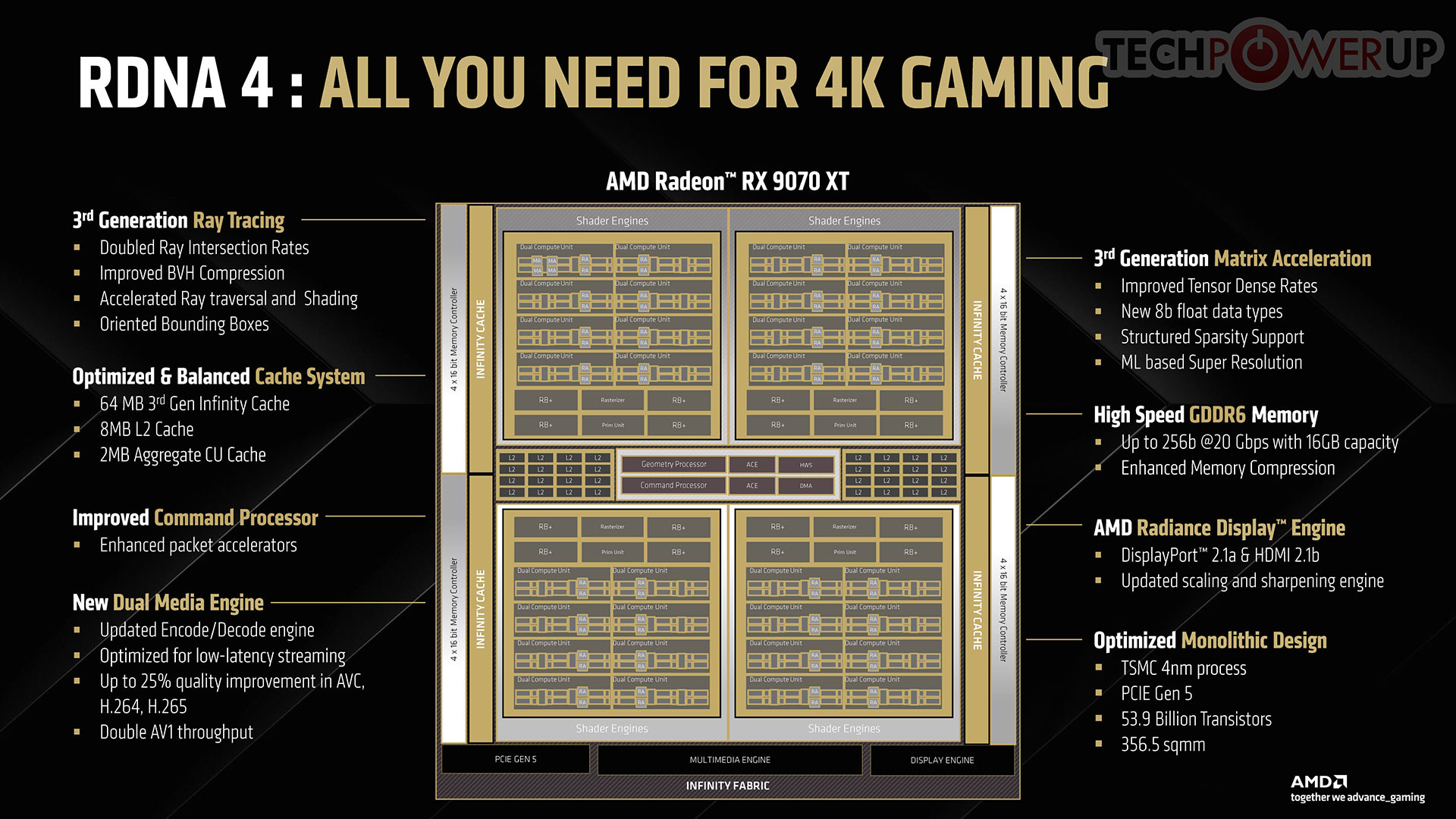

The new Radeon RX 9070 XT and RX 9070 are powered by the 4 nm Navi 48 silicon. Unlike the Navi 31 and Navi 32 before it, this is a traditional monolithic die built entirely on the TSMC N4P (4 nm EUV) process node. It has an area of 356.5 mm², but with an impressive transistor count of 53.9 billion. To put this number into context, the previous "big Navi" GPU, the Navi 31 powering the RX 7900 XTX, has 57.8 billion transistors (just 8% more), despite having 96 CU, a larger Infinity Cache, and a wider 384-bit memory bus. Navi 31 has a die area of 529 mm² (304 mm² for the 5 nm GCD, with the rest being 6 nm MCDs), so you can see the kind of strides AMD made with die-area. At the top-level, the Navi 48 features a PCI-Express 5.0 x16 host interface and a 256-bit wide GDDR6 memory bus. With 20 Gbps GDDR6 memory chips, the RX 9070 XT gets 640 GB/s of memory bandwidth. This is made up for with a faster 64 MB Infinity Cache, and a critical improvement AMD made to its memory management system, called Out-of-Order Memory Queuing.
The Navi 48 silicon physically has 64 CU spread across 4 shader engines. With each CU containing 64 stream processors, the chip has a total of 4,096 stream processors. All 64 CU are enabled on the RX 9070 XT, while the RX 9070 has 56 out of 64 of them enabled. The maxed-out Navi 48 contains 4,096 stream processors, 128 AI accelerators, 64 RT accelerators, 256 TMUs, and 128 ROPs. The chip also features 64 MB of 3rd Gen Infinity Cache, and a 256-bit wide GDDR6 memory interface, driving 16 GB of 20 Gbps memory on both the RX 9070 XT and RX 9070. With 56 CU enabled on the RX 9070, it has 3,584 stream processors, 112 AI accelerators, 56 RT accelerators, 224 TMUs, and an untouched ROP count of 128, besides the exact same memory configuration as the RX 9070 XT.
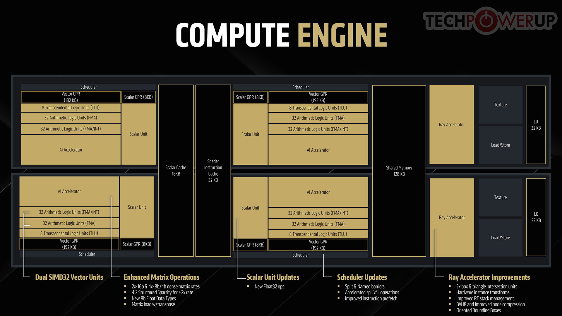
At the heart of the RDNA 4 graphics architecture is the new dual compute unit, with a vastly improved memory sub-system, improvements made to the scalar units, a new technology called dynamic register allocation, and improvements to CU efficiency and engine clocks. Each CU has two scheduler blocks, driving a 192 KB general purpose register (GPR), an 8 KB scalar GPR, 32 FMA ALUs, and 32 FMA+INT ALUs. There are also 8 transcendental logic units. RDNA 4 introduces the concept of dual SIMD32 vector units, for even more parallelism. The Scalar Unit comes with support for newer Float32 ops. Schedulers are updated with accelerated spill/fill operations. Instruction prefetching is improved. The new generation AI Accelerator comes with two 16-bit and four 8-bit/4-bit dense matrix compute rates, support for 4:2 structured sparsity for doubling throughput, and matrix loads with transpose. AMD has incorporated many technologies from its CDNA 3 Radeon Instinct AI ML accelerators on the AI Accelerators of RDNA 4, including enhanced and power-optimized WMMA, improvements to the ops per CU, support for FP8, E4M3 and E5M2 formats, and 4:2 structured sparsity.
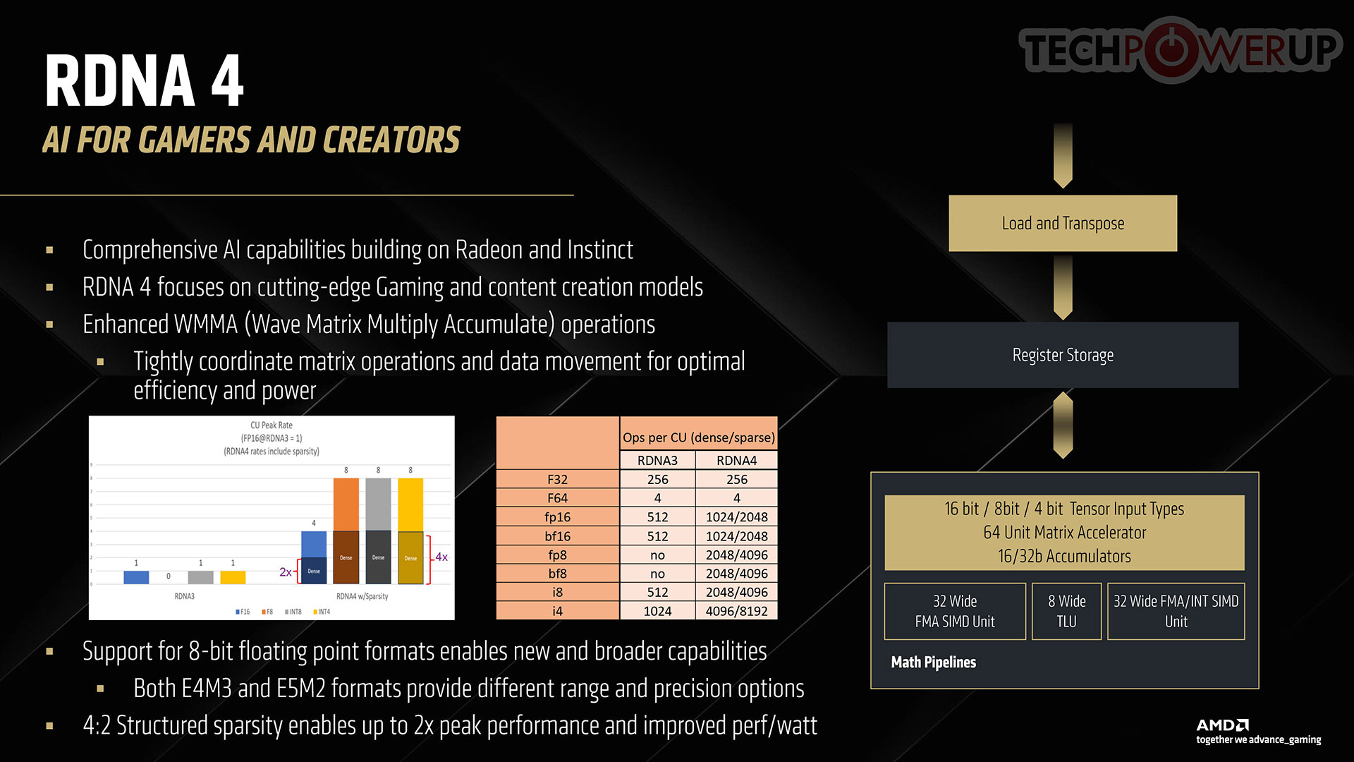
The new generation AI Accelerator comes with two 16-bit and four 8-bit/4-bit dense matrix compute rates, support for 4:2 structured sparsity for doubling throughput, and matrix loads with transpose. AMD has incorporated many technologies from its CDNA 3 Radeon Instinct AI ML accelerators on the AI Accelerators of RDNA 4, including enhanced and power-optimized WMMA, improvements to the ops per CU, support for FP8, E4M3 and E5M2 formats, and 4:2 structured sparsity.
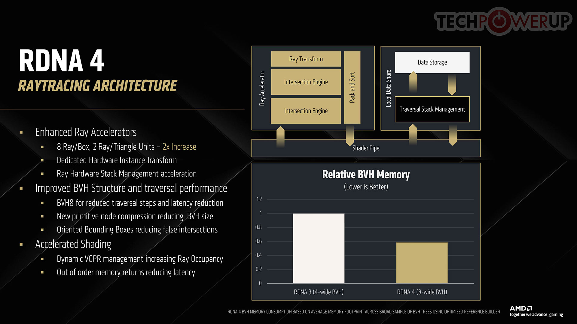
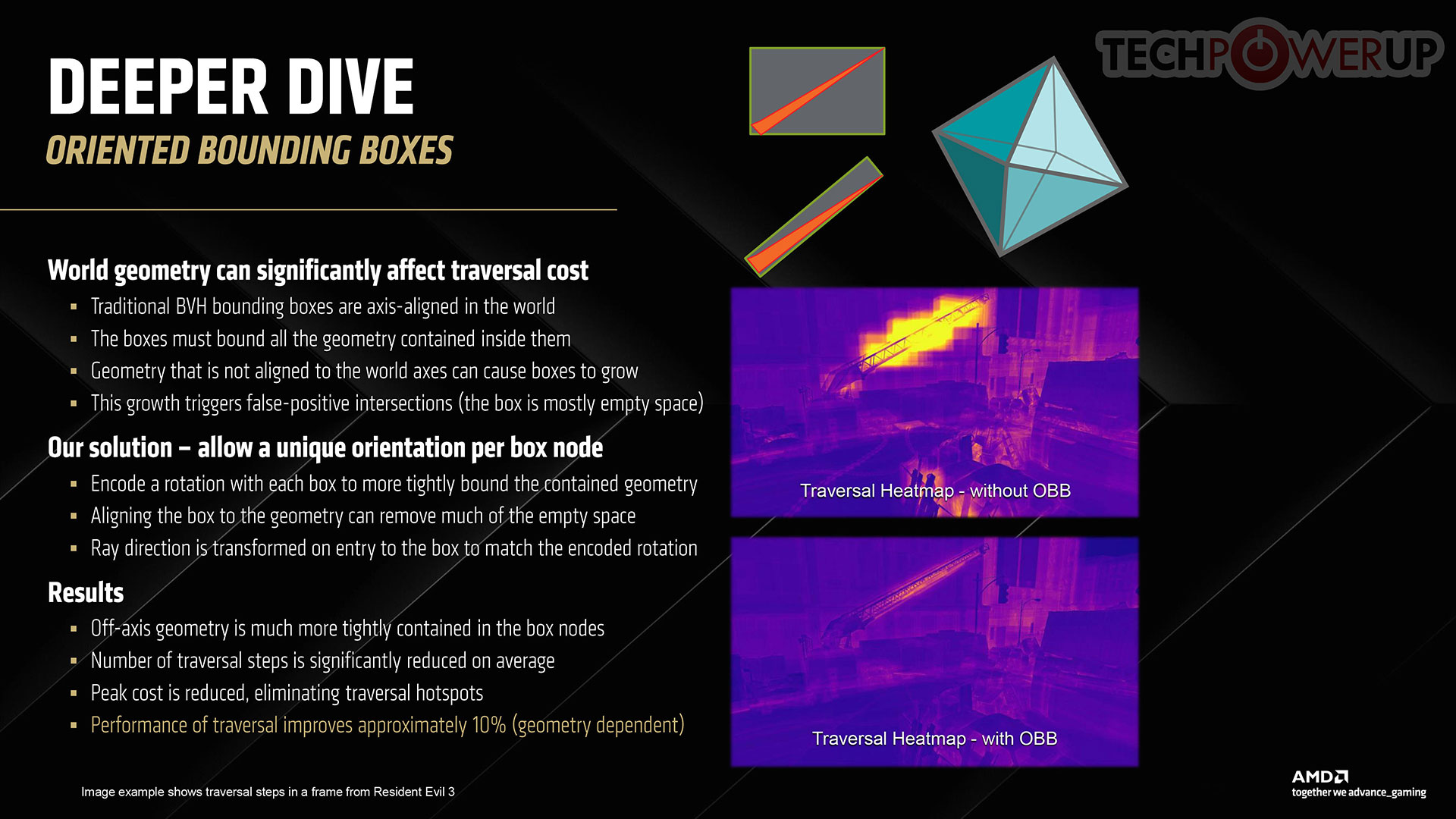
The new generation Ray Accelerator comes with double the box and triangle intersection resources as RDNA 3 RT accelerator, support for hardware instance transforms, improvements to the RT stack management, BVH8 node compression, and a revolutionary feature called oriented bounding boxes. To contain the number of rays really needed to be tested against an object, modern ray tracing technologies use something called a bounding box, which defines a region in which a geometry has to be tested against rays. Most of the time, the geometry is of a vastly different shape and smaller than the shape of a bounding box, which introduces false intersections, and wastes ray testing resources. AMD innovated a way to turn this bounding box into a 3D shape by giving it a Z-axis component, so the bounding box is oriented closer to the shape of the object to be tested, reducing the number of rays needed to be tested against it.
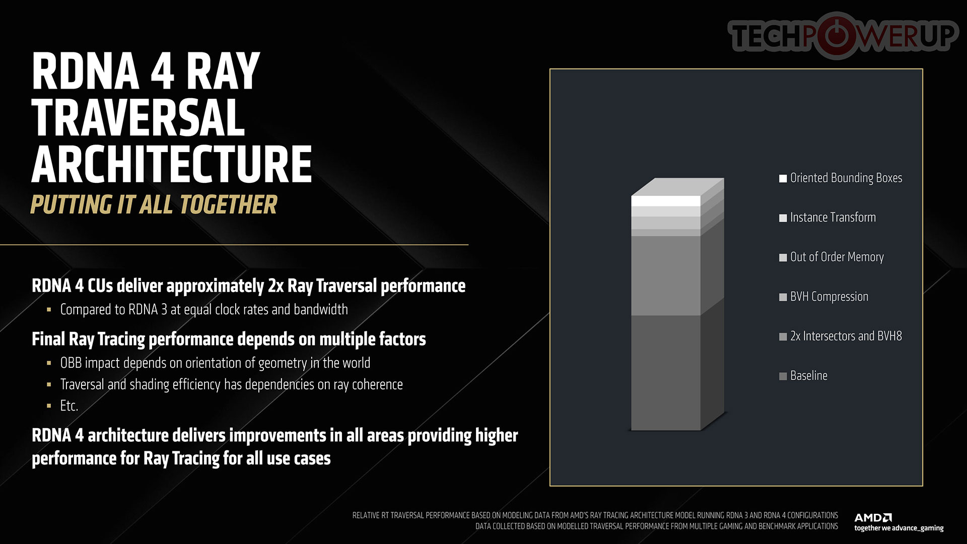
This graph highlights the contribution of various components toward the 100% generational ray traversal performance gain, allowing AMD to make do with a CU count of 64, with RDNA 3 being the baseline.
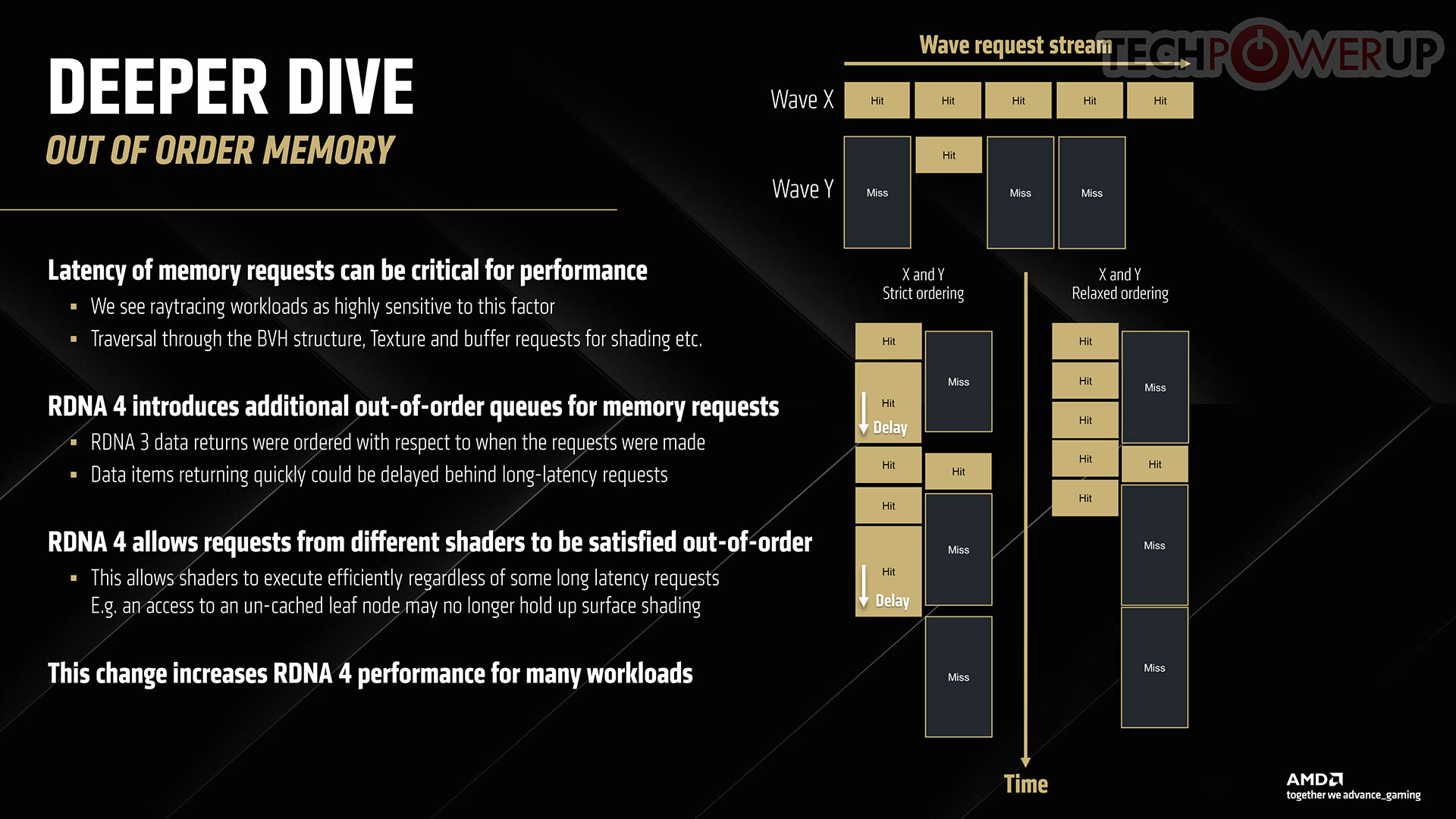
Both ray tracing and ML acceleration are memory sensitive applications, so AMD innovated a revolutionary change to its memory management system with the introduction of new out-of-order memory. All math is executed in waves on an RDNA GPU, and mutual dependencies between waves can cause memory request stream misses, as one wave's memory request queue waits for the other wave to complete its task. This is solved with a new out-of-order (relaxed ordering) memory management. This graph highlights the contribution of various components toward the 100% generational ray traversal performance gain, allowing AMD to make do with a CU count of 64, with RDNA 3 being the baseline.
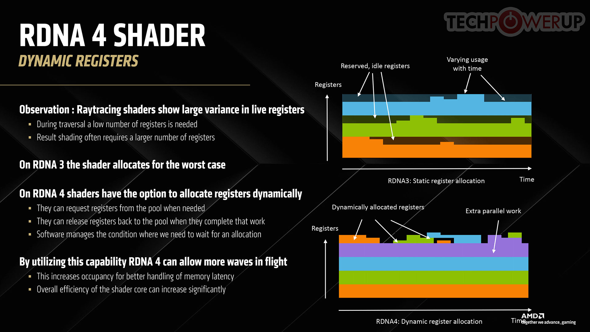
On AMD, a fairly big chunk of the ray tracing stack continues to be executed on shaders, but the company has made advances to ensure the cost of ray tracing on the shader resources of the GPU is minimal, with the introduction of Dynamic Registers to improve parallelism.
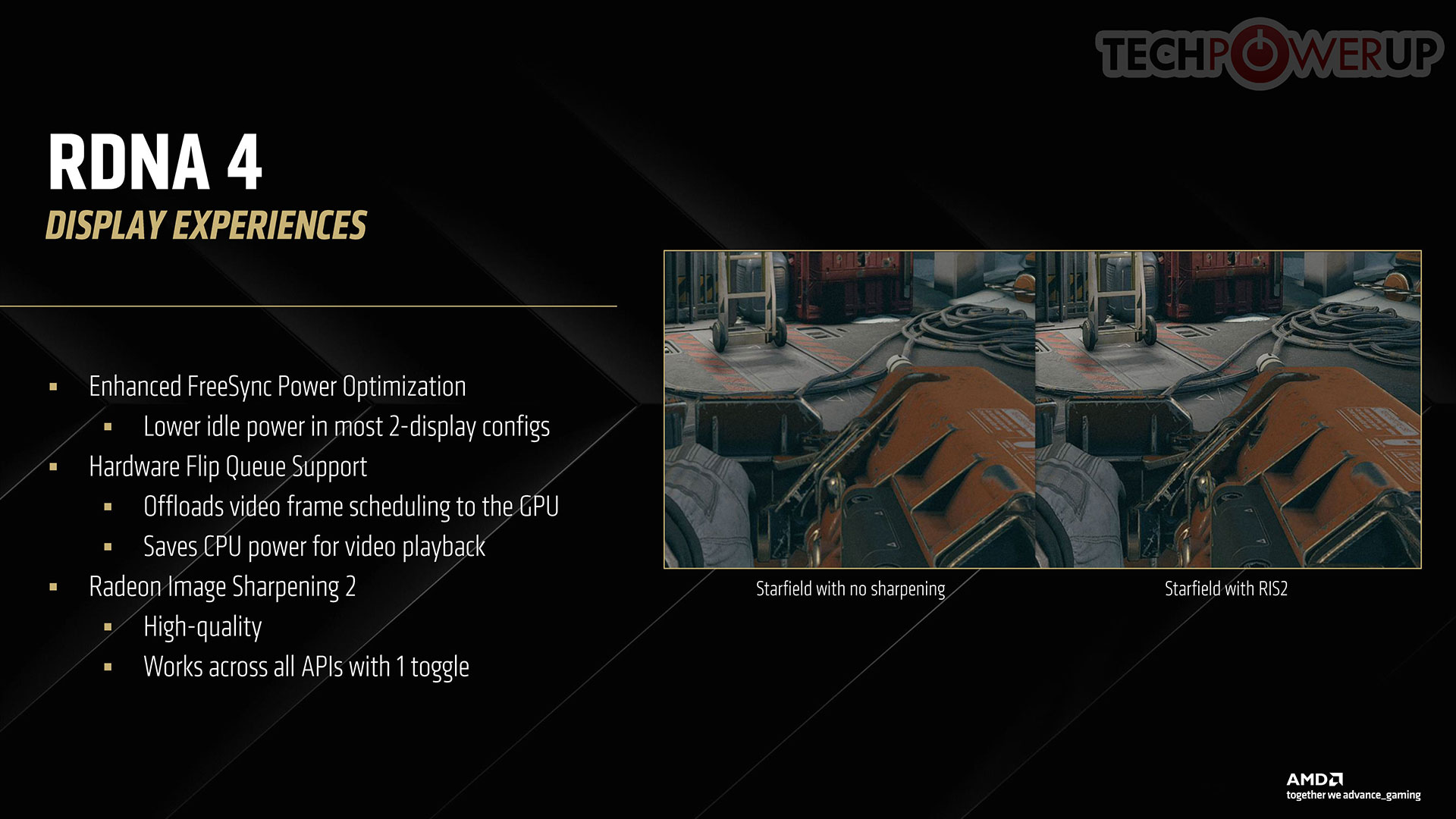
The new Radiance 2 Display Engine comes with major hardware updates that reduce GPU idle power draw in multi-monitor setups. The engine also comes with hardware flip-metering support (something NVIDIA also introduced with Blackwell, and which enables Multi-Frame Gen on the RTX 50-series). Flip-metering improves video frame pacing to the GPU and reduces CPU overhead for video playback. There is also a display engine level hardware image sharpening component that drives Radeon Image Sharpening. As for I/O, you get contemporary DisplayPort 2.1a and HDMI 2.1b, we are waiting to confirm the UHBR bit-rates.
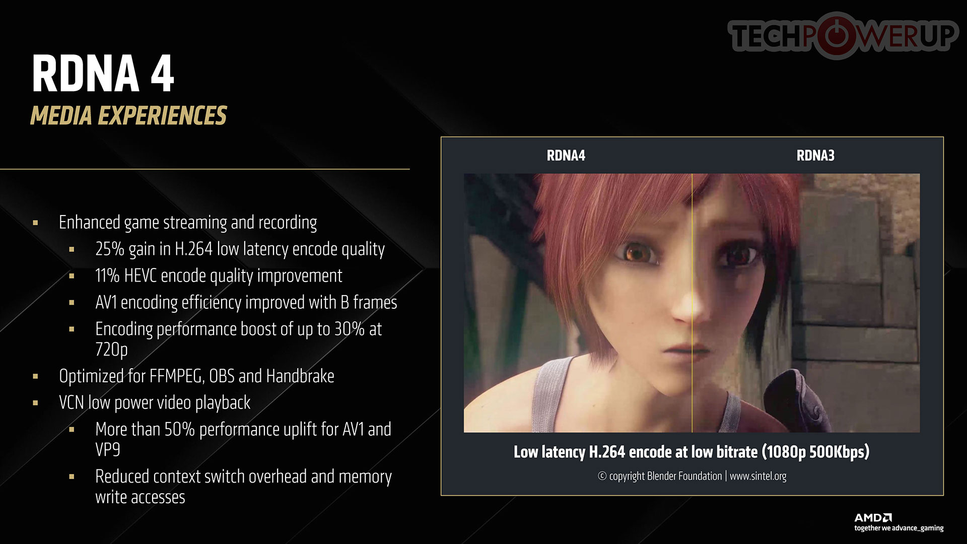
Navi 48 comes with a dual media engine, each of the two can perform concurrent encoding and decoding, and so the implementation resembles an NVIDIA GPU having two each of NVENC and NVDEC units. The new generation media engine offers a 25% increase in H.264 low-latency encode quality, and an 11% improvement in HEVC encode quality. AV1 encode and decode get B-frames support, vastly improving bitrates. The media engine posts a 50% generational performance uplift (measured in encoder/decoder frame rates), with reductions in memory overhead.
AMD FSR 4 and New AMD Software Features
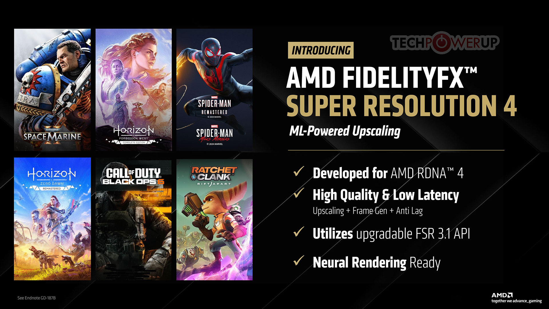

With the Radeon RX 9000 series, AMD is debuting FSR 4, the latest version of its performance enhancement suite. FSR 4 introduces the biggest tech update since FSR 2, which also makes it exclusive to the RX 9000 series. With the RDNA 4 generation of GPUs offering significantly higher ML compute throughput, AMD designed a new ML-based upscaler to reconstruct details of the upscaled frame. In that sense, FSR 4 is technologically close to DLSS. RDNA 4 GPUs also leverage AI DNNs to de-noise ray tracing and path tracing, unburdening the shaders.
An AI ML based upscaler requires ground truth data, and just as NVIDIA goes through the painstaking task of training game-specific ML models that can later be shipped to end-users through game developers and as driver updates; AMD has set up a large FSR 4 data-center of its own, powered by Radeon Instinct MI300-series AI GPUs for the task. On the client side, the ML-based upscaler needs the dedicated AI acceleration hardware from the RDNA 4 family. The frame generation technology appears to be carried over from FSR 3 Frame Generation, and is essentially a smart frame interpolation technology.
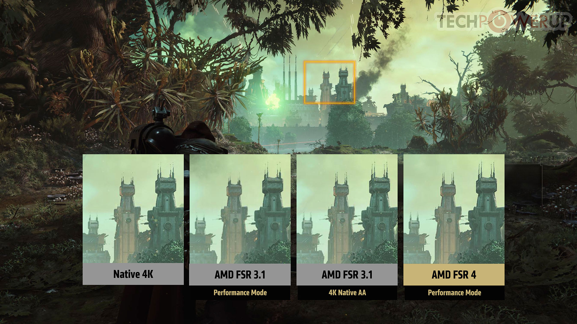
AMD in its presentation provided examples of image quality for FSR 4, claiming that in some cases, FSR 4 presents geometry more accurately than even native resolution. While AMD didn't detail it, FSR 4 comes with preparation for neural rendering. Given that Microsoft has now standardized neural shaders, and the ability for applications to directly address AI acceleration hardware on the GPU via the DirectX API, AMD could in the near future implement neural rendering, however, the company hasn't detailed a timeline. FSR 4 is ready for neural rendered objects.
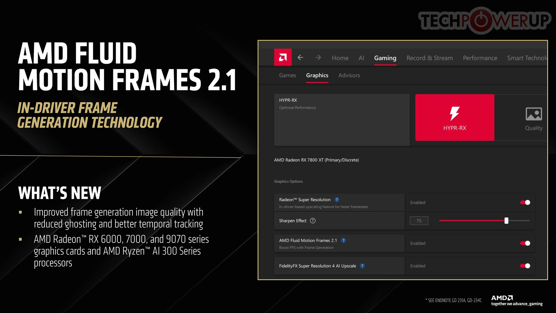
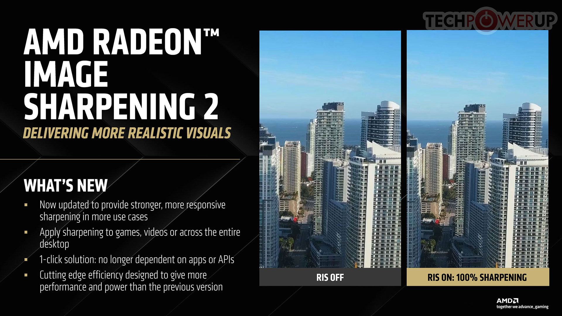
Fluid Motion Frames gets an update with FMF 2.1, with improved image quality, reduced ghosting, and improved temporal tracking. The company also updated its API-agnostic image sharpening tool, with the introduction of Radeon Image Sharpening 2 (RIS 2).
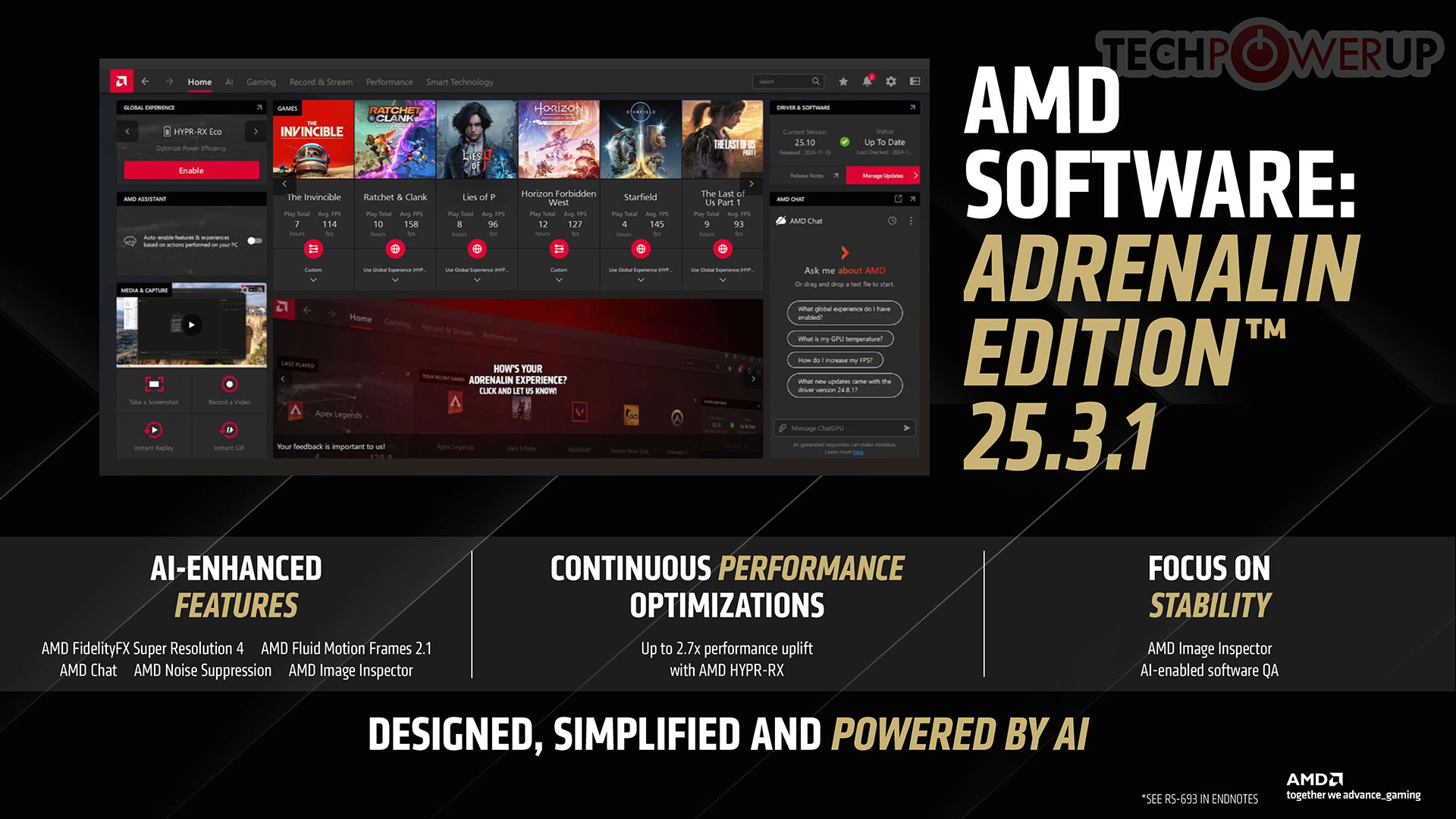
AMD provides a slick driver frontend application called simply "AMD Software." AMD improved the way in which users can report bugs, artifacts, or corruption in games, through a voluntary (opt-in) feature called AMD Image Inspector.
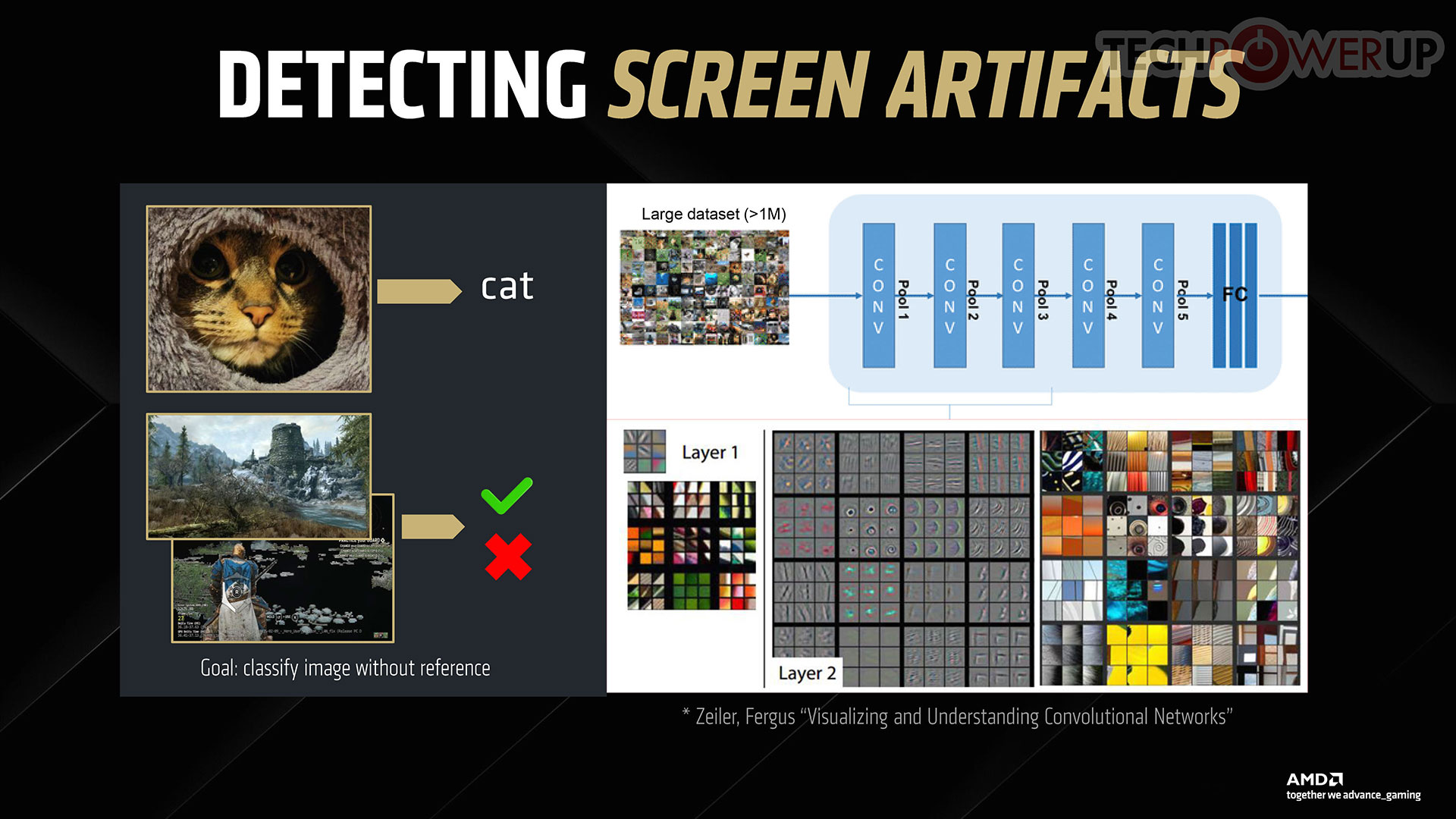

As you submit a screenshot or video sequence to AMD, the company uses an AI model to identify rendering bugs, or corruption in the display. The entire driver-level game optimization, testing, and bug fixing process has been revamped with AI doing the heavy lifting.
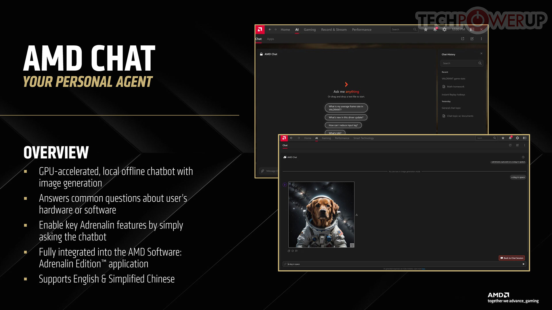
The company also introduced AMD Chat, which is an AI chatbot that runs locally, and is accelerated by the GPU. You can make plain language queries on configuring AMD Software features and settings; and also chat with it on AMD technologies. This is essentially AMD's answer to NVIDIA's ChatRTX, but we don't know if the utility can be trained with custom datasets.
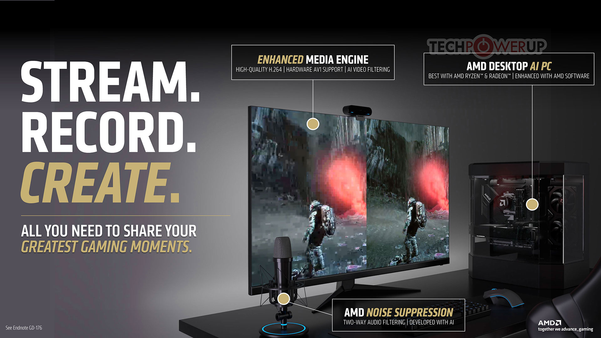
For streamers, AMD Software simplifies connecting their gameplay with their social media and streaming accounts. You can then take advantage of the new dual media engine of RDNA 4 that improves H.264 and HEVC image quality, and use other utilities such as AMD Noise Suppression, which is a 2-way AI-based audio filter.
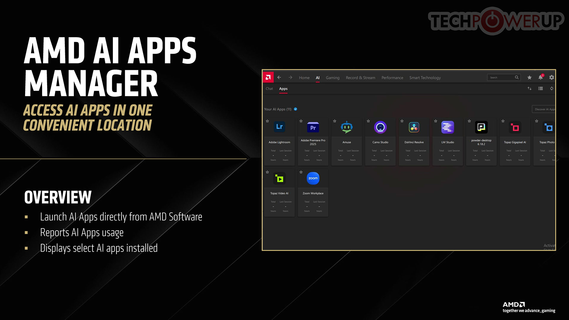
AMD AI Apps Manager consolidates all your AI applications into a simple launcher-like interface resembling a game launcher.
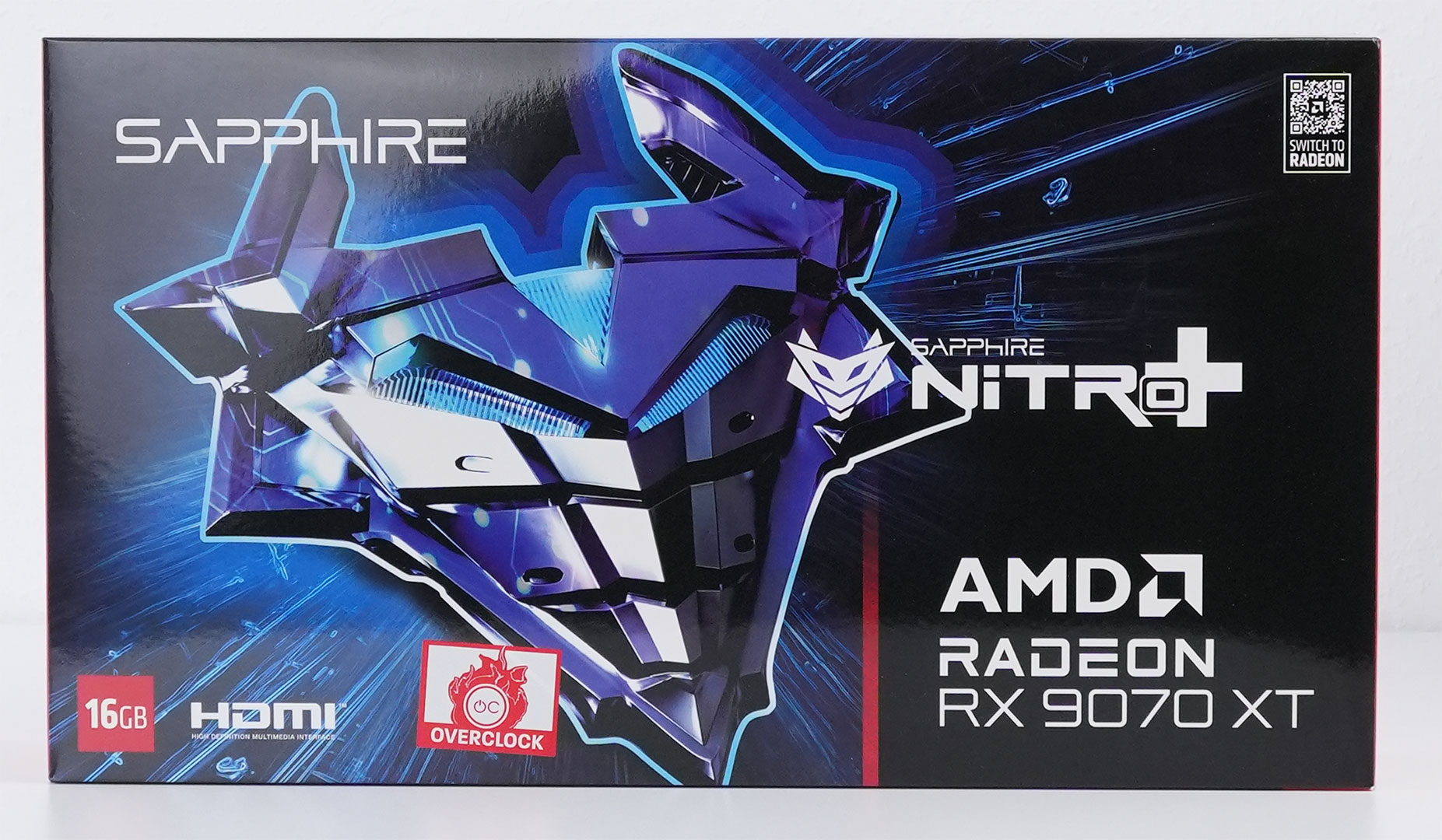
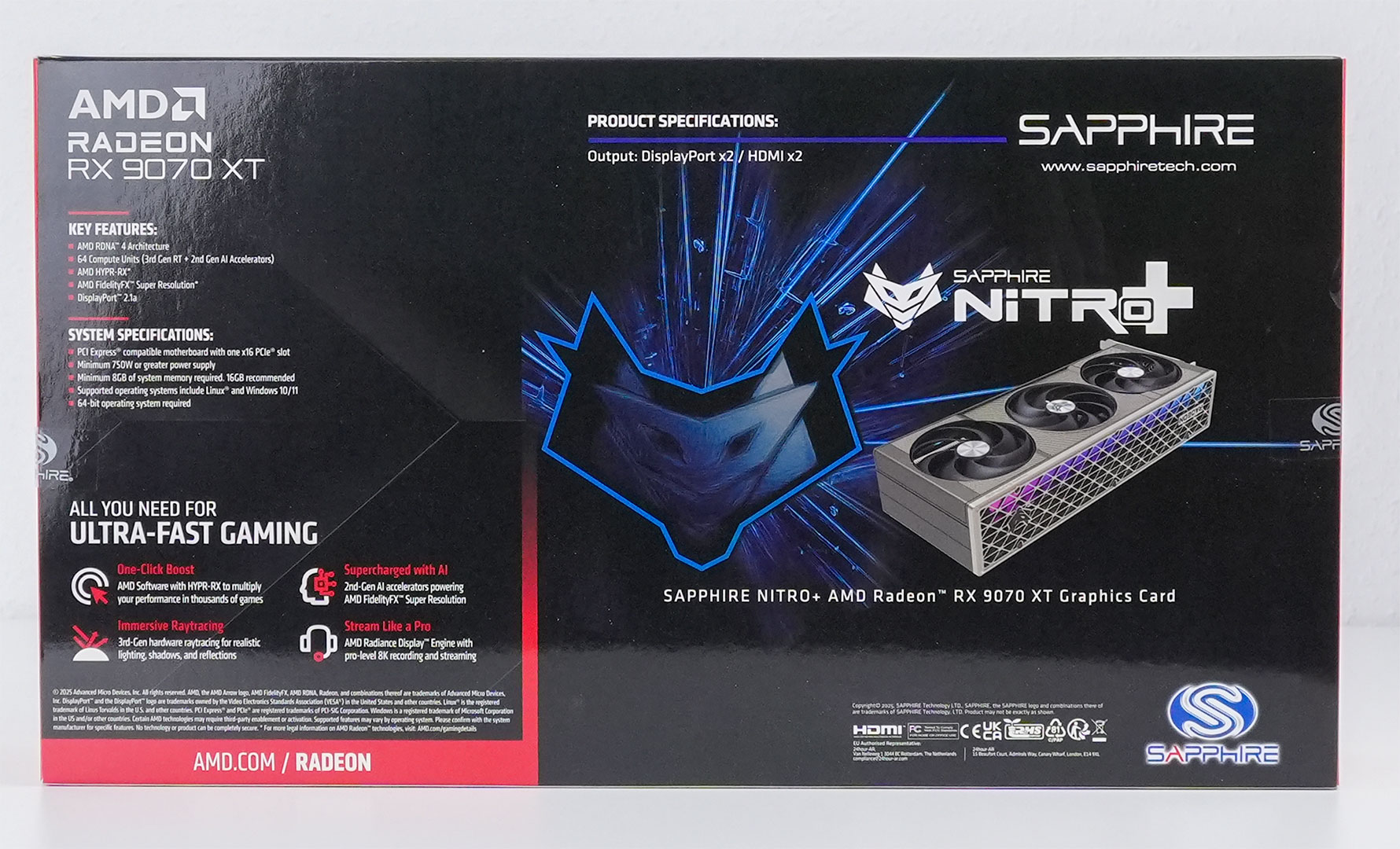
Packaging
The Card
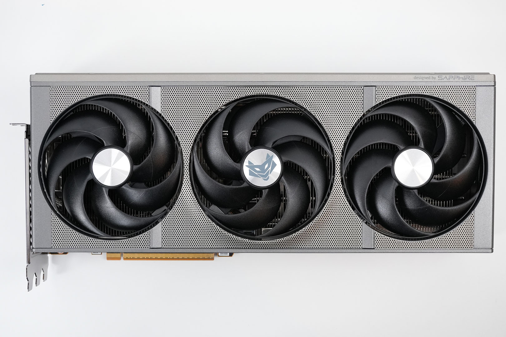
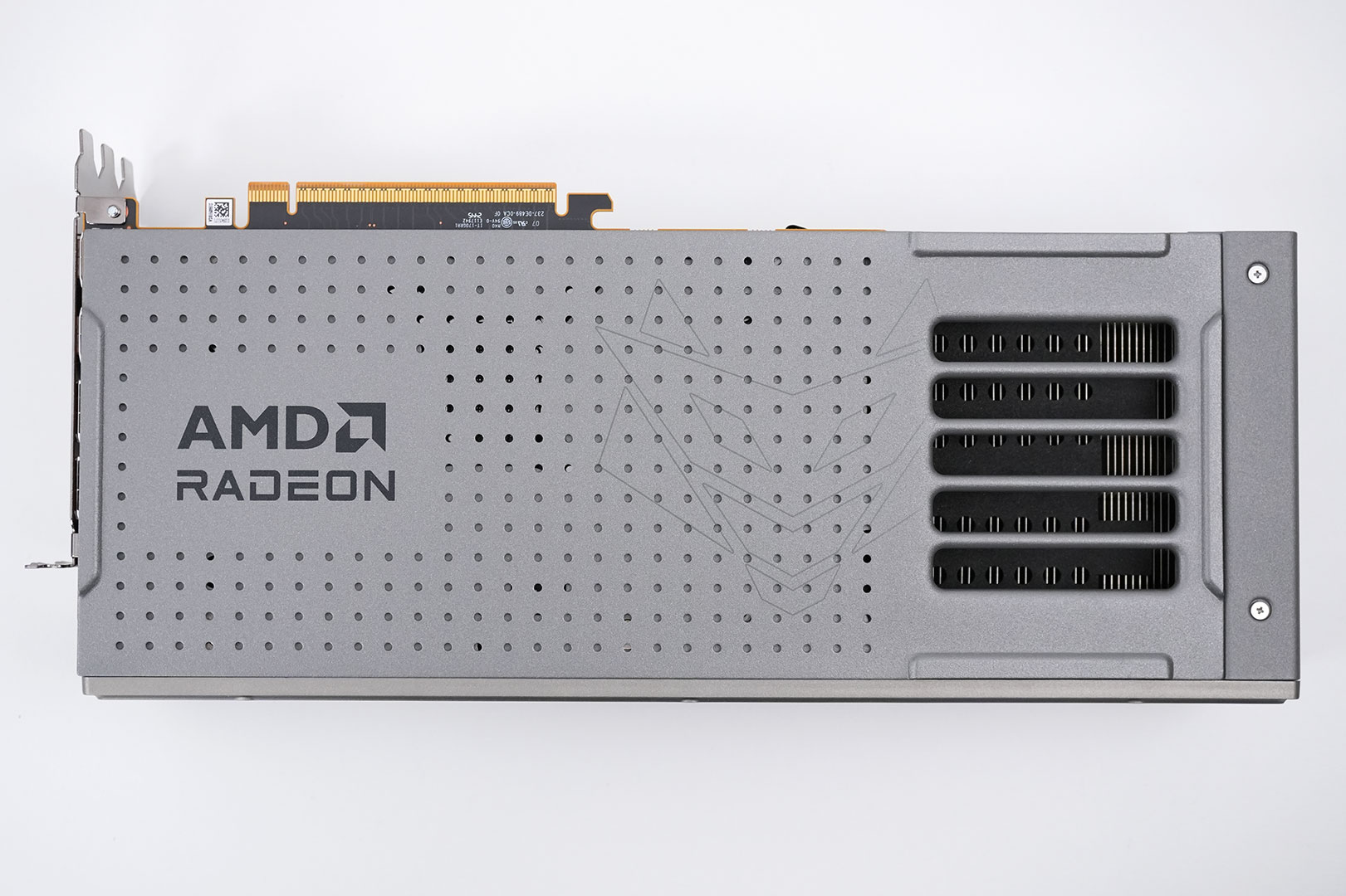
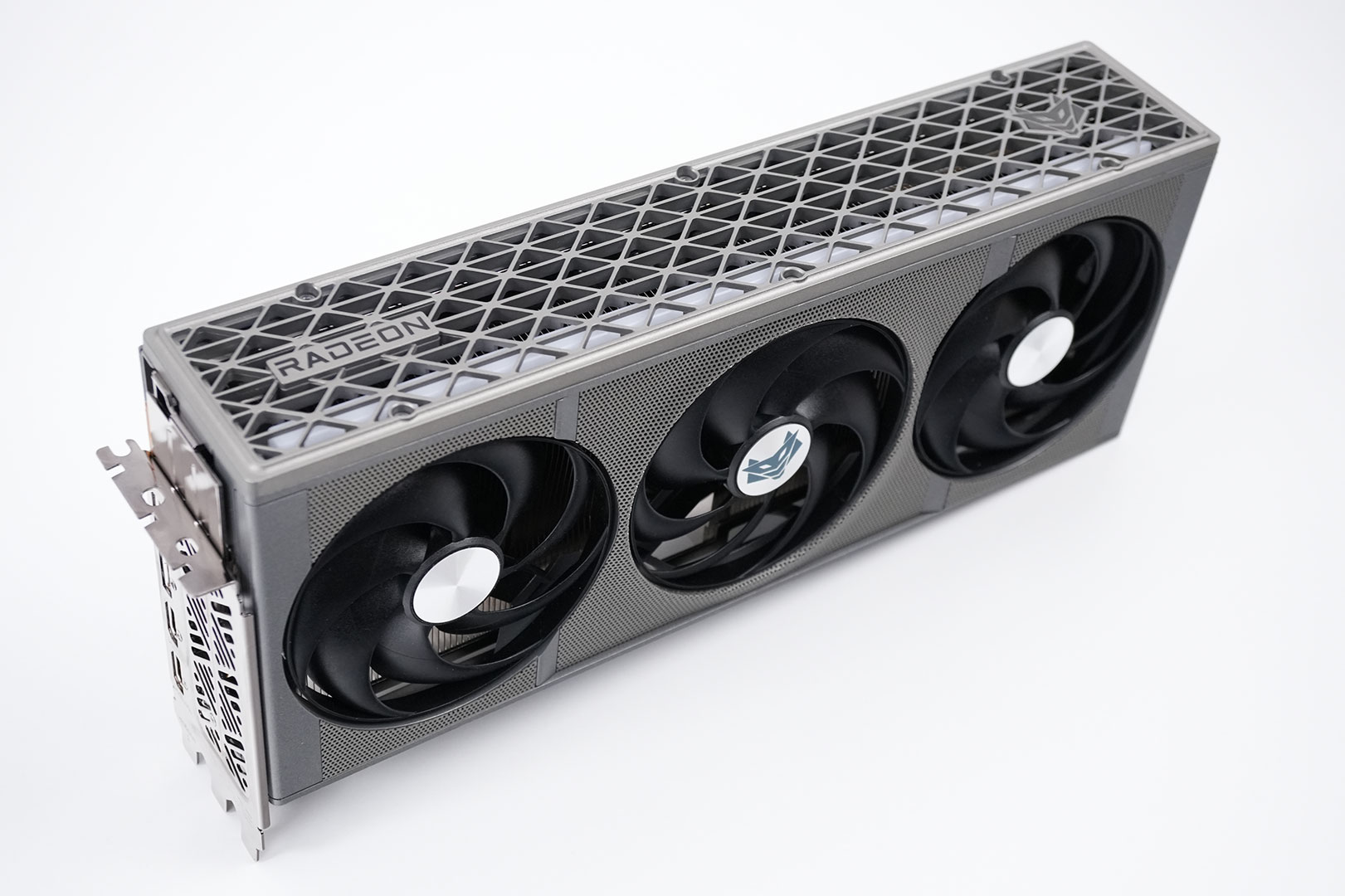
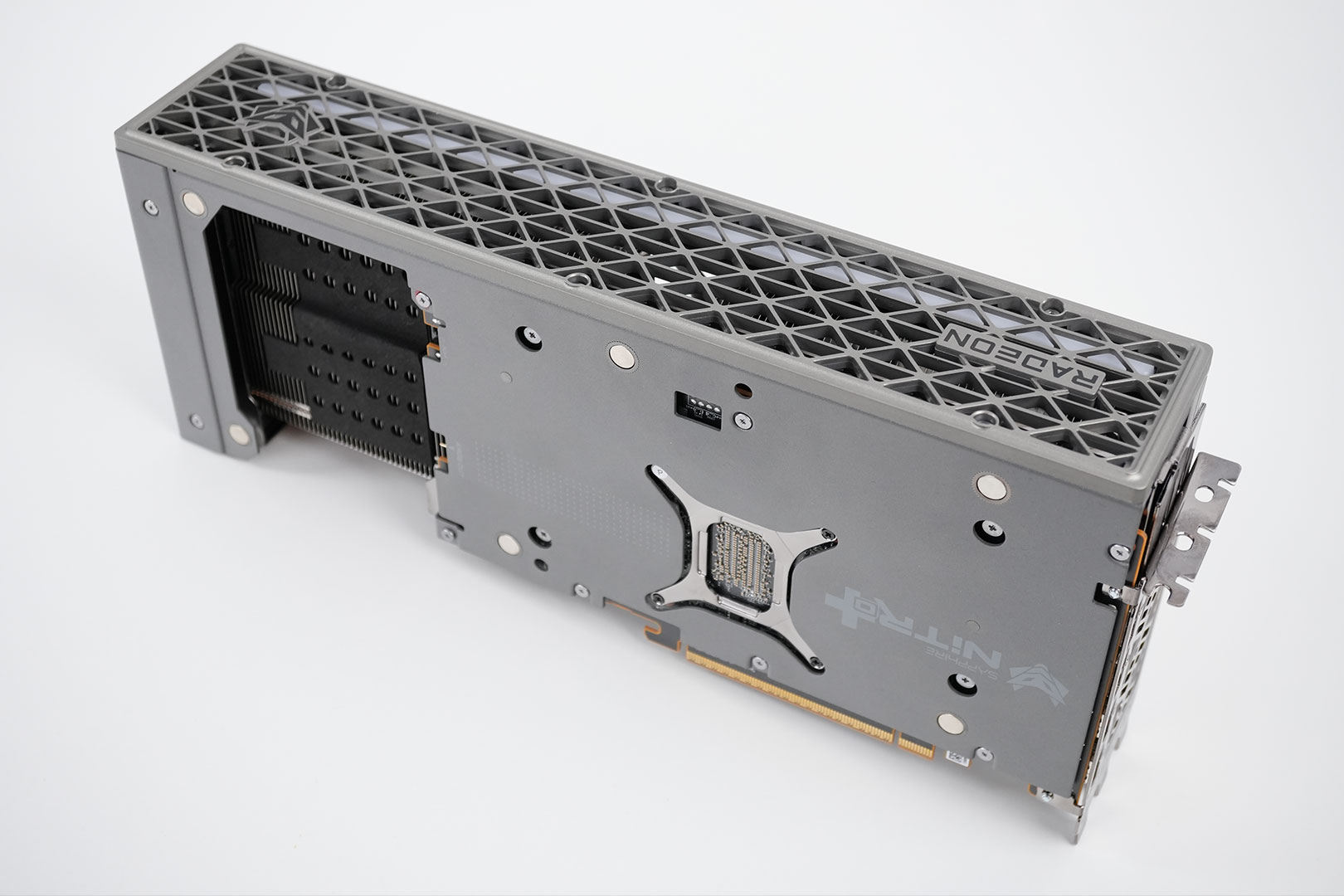
Sapphire is introducing a new design theme for the Nitro of this generation. The main color is gray, but there are several highlights. The backplate is attached magnetically and is used to cover the power connector area and hide the cables—great idea!
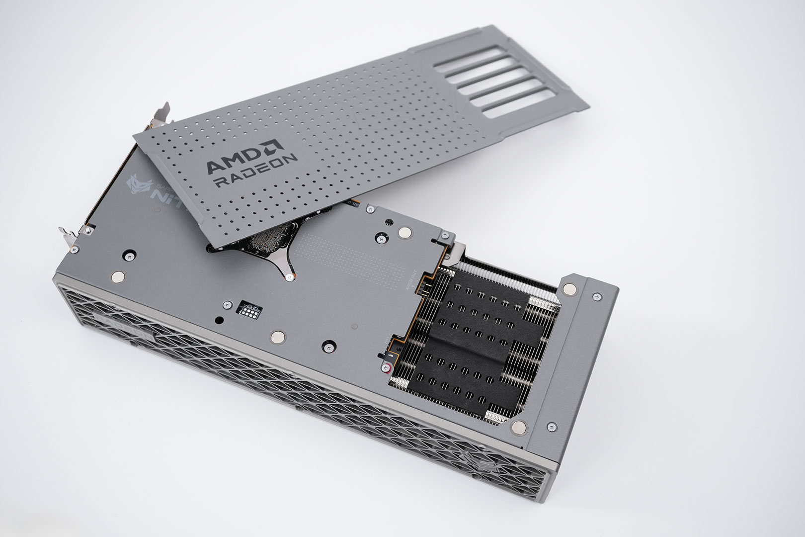

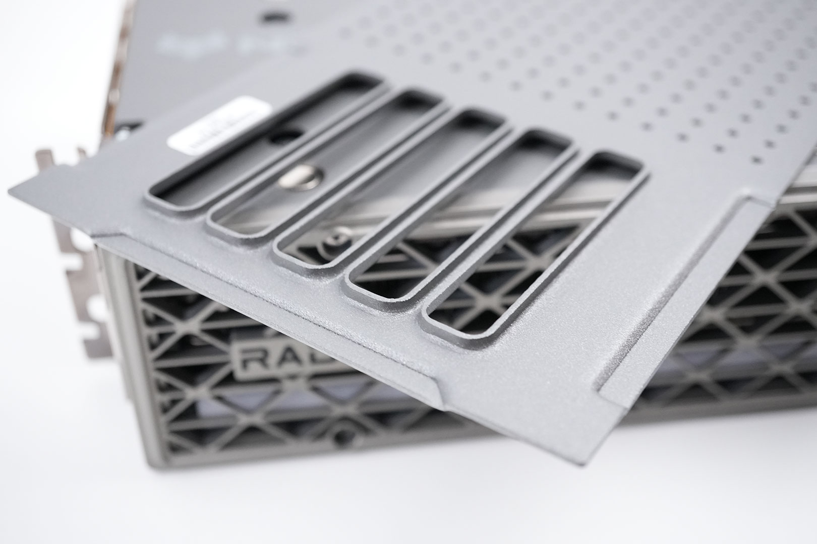
The cover is made from thick metal and uses a tool-free magnetic attachment mechanism.
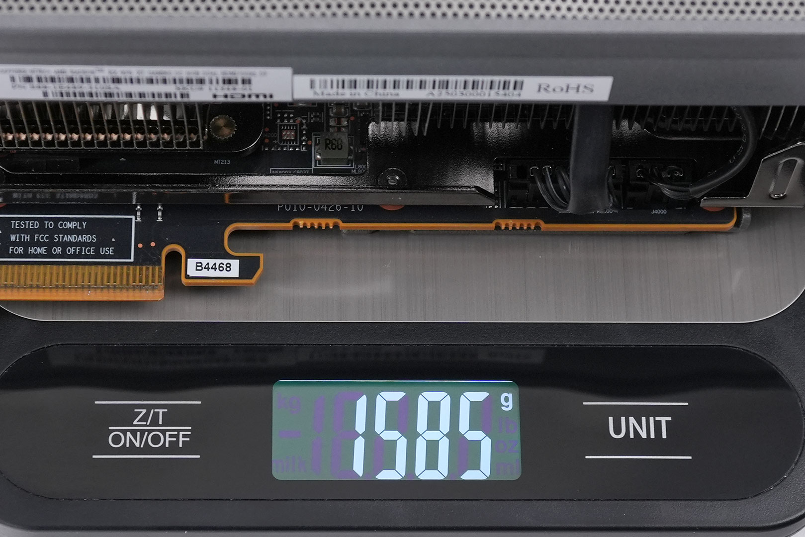
Dimensions of the card are 33.0 x 14.0 cm, and it weighs 1585 g.
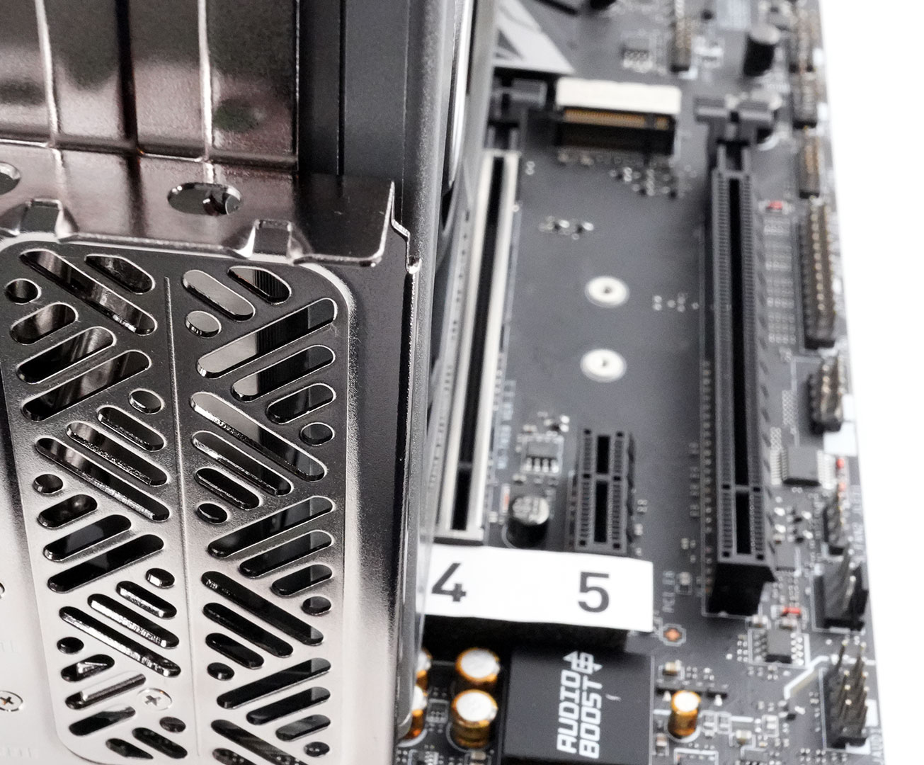
Installation requires three slots in your system. We measured the card's width to be 64 mm. You can really fit an addon card in the free slot—I tested it.

Display connectivity includes two standard DisplayPort 2.1b and two HDMI 2.1b. With RDNA 4, AMD put effort to improve its standing with game streamers and creative professionals. It's done this by giving Navi 48 a dual VCN solution, so the GPU has two concurrent hardware accelerators for encoding and decoding. Perhaps the biggest changes at the silicon level is that AMD improved the encoding quality of its hardware H.264 and HEVC codecs. This was a niche complaint streamers had with AMD GPUs, who would avoid the brand altogether. The company also updated its AV1 hardware acceleration with support for B-frames, which are frames that lack image information, but have math data that let the decoder reconstruct image data by comparing with the image data from adjacent I-frames containing it. This technique vastly improves streaming bitrates since half the frames lack image data.
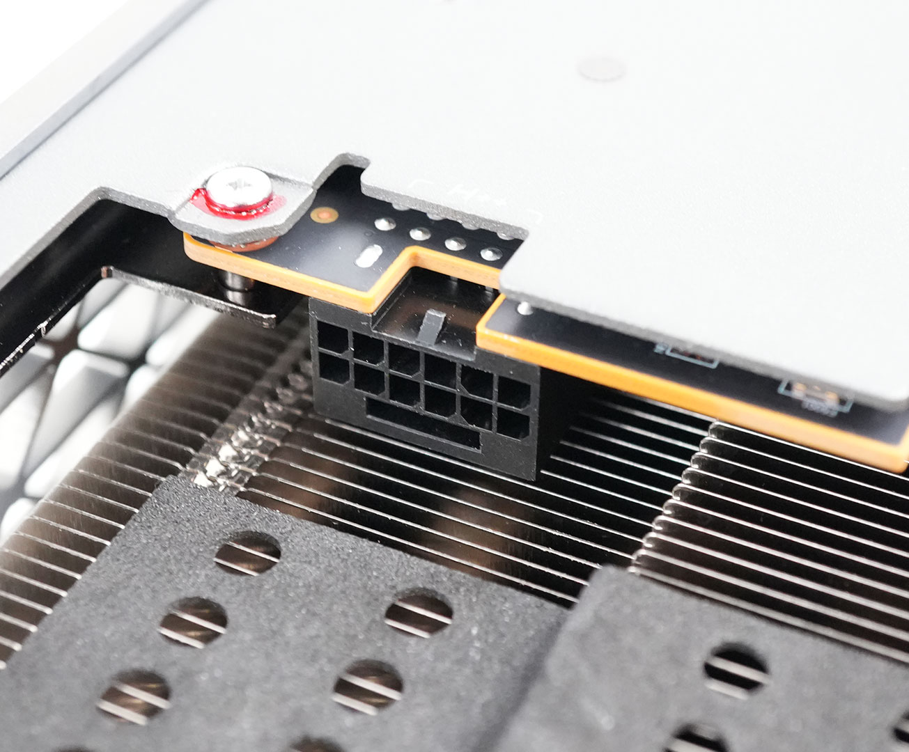
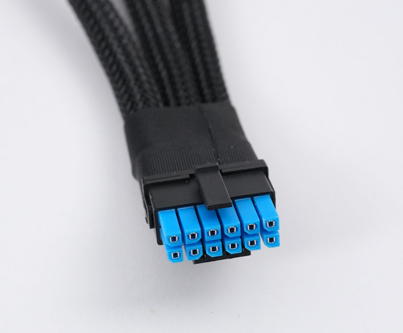
The card uses a single 16-pin connector, which is located near the back of the card, a much better location than along the side like on the various NVIDIA cards.
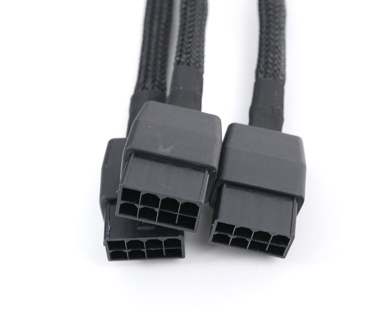
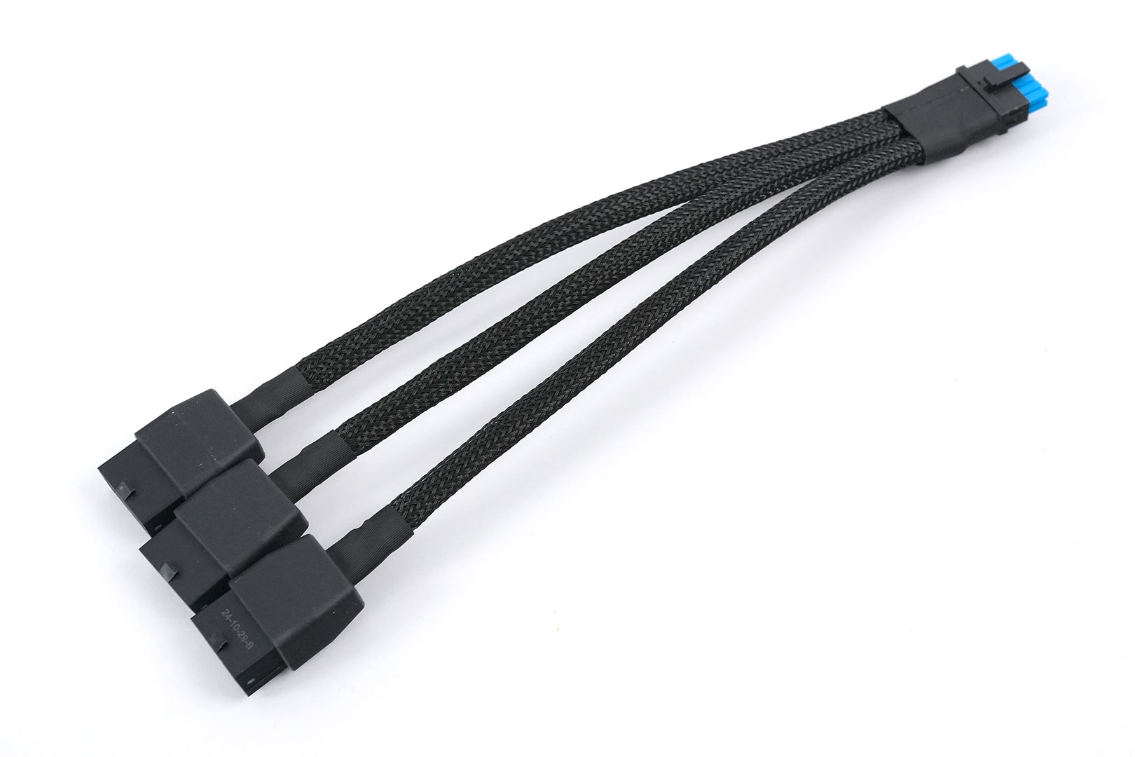
This adapter cable is included in the box, to convert three 8-pins into a 16-pin.
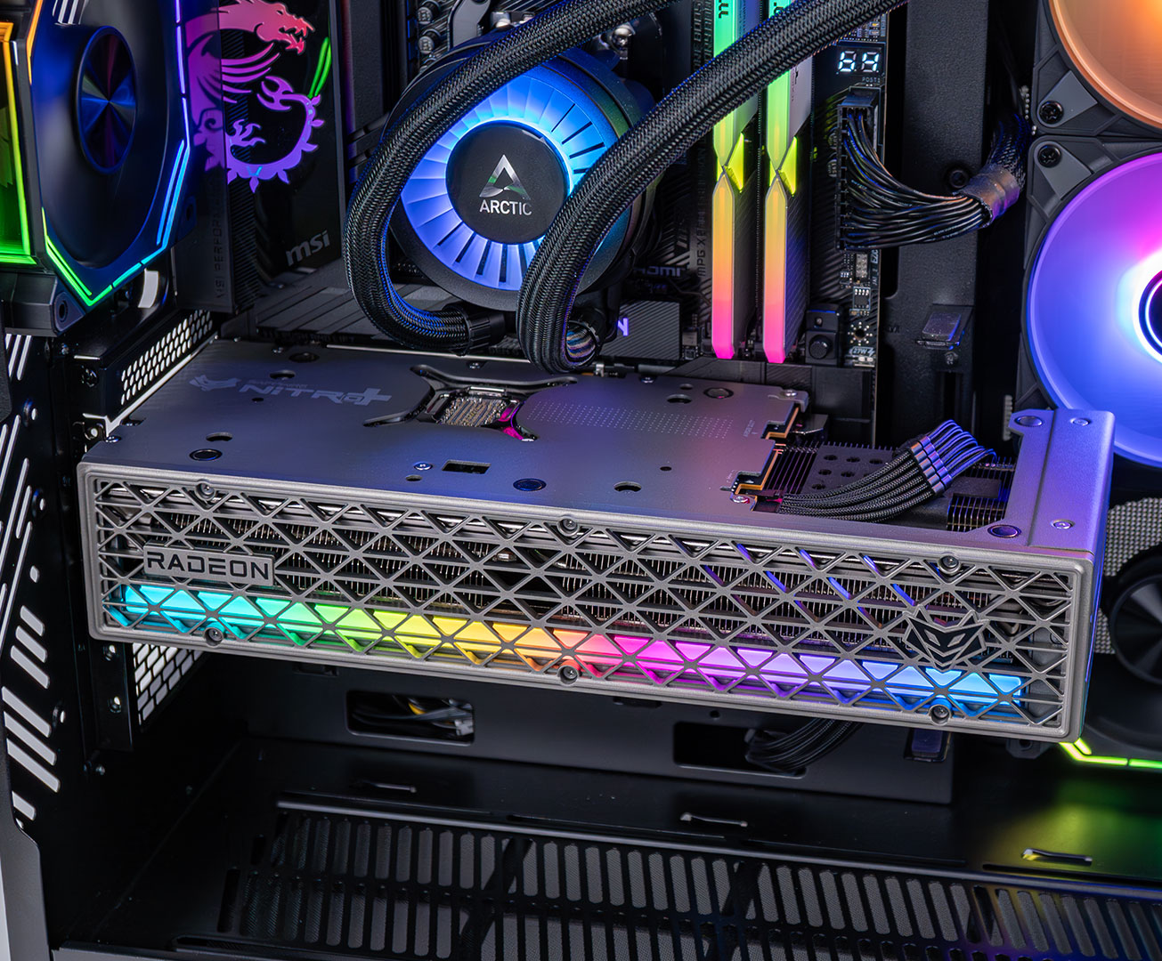
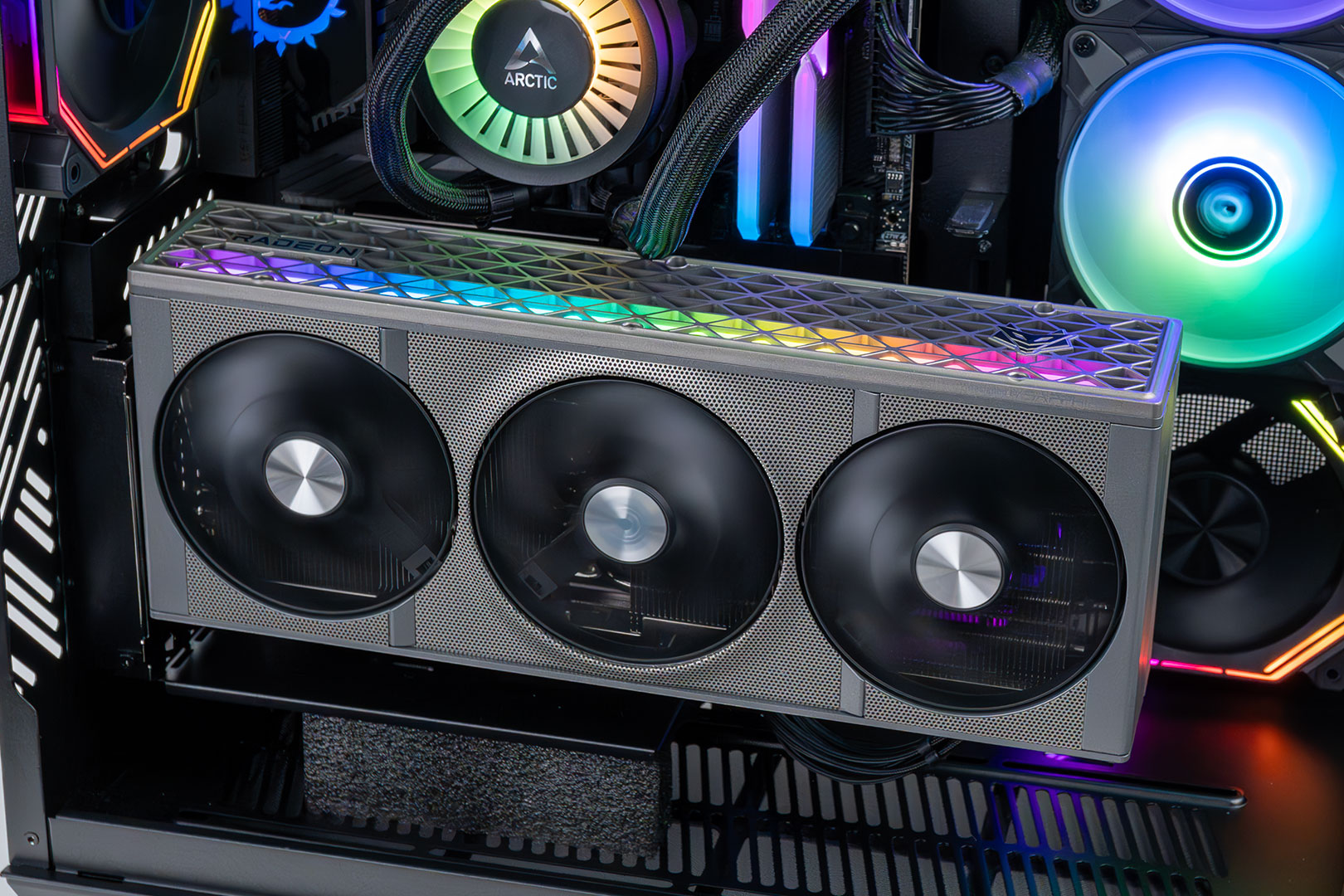
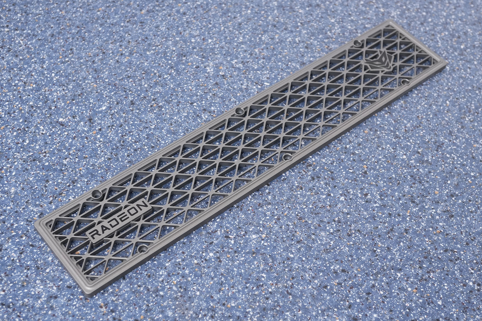
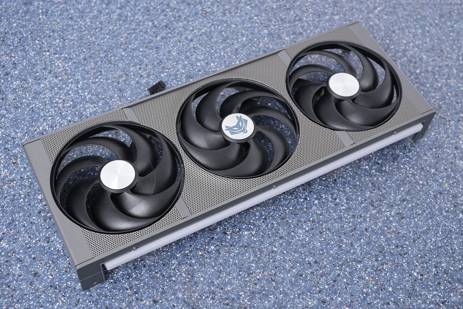
Sapphire has installed an RGB lighting zone along the top edge of the card.
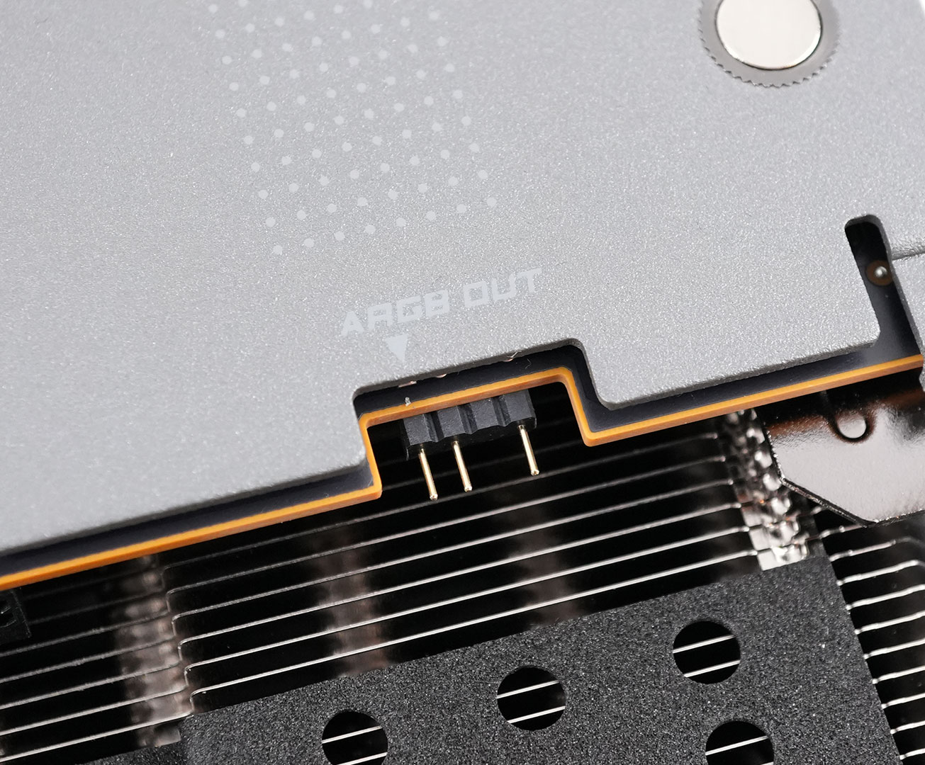
This connector is used to synchronize the lighting of your system with the graphics card.
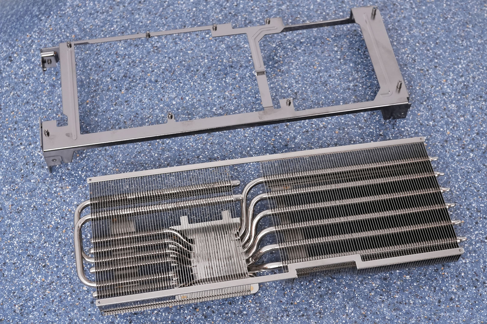
Teardown
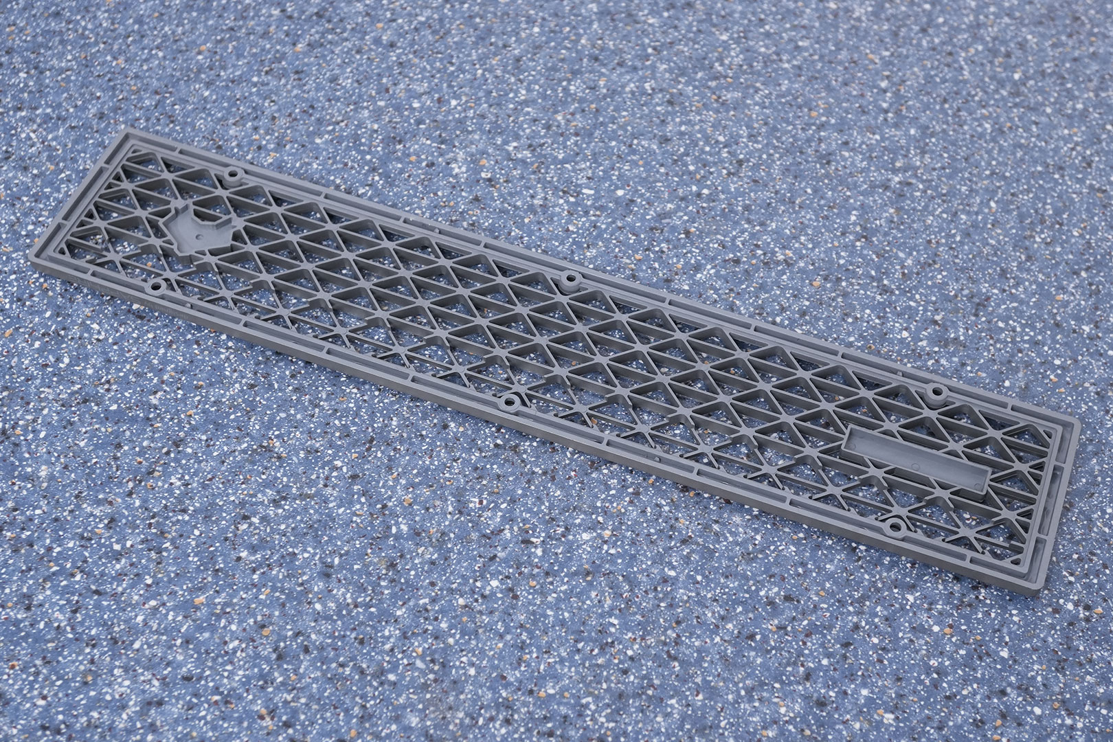
The plastic frame goes off first, it helps reinforce the card against bending, too.
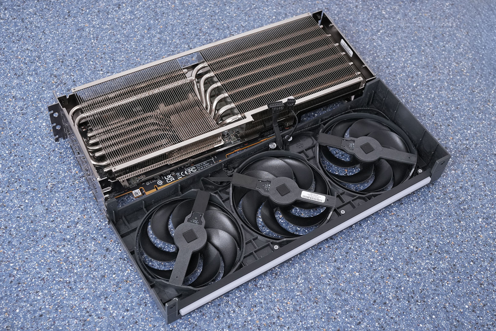
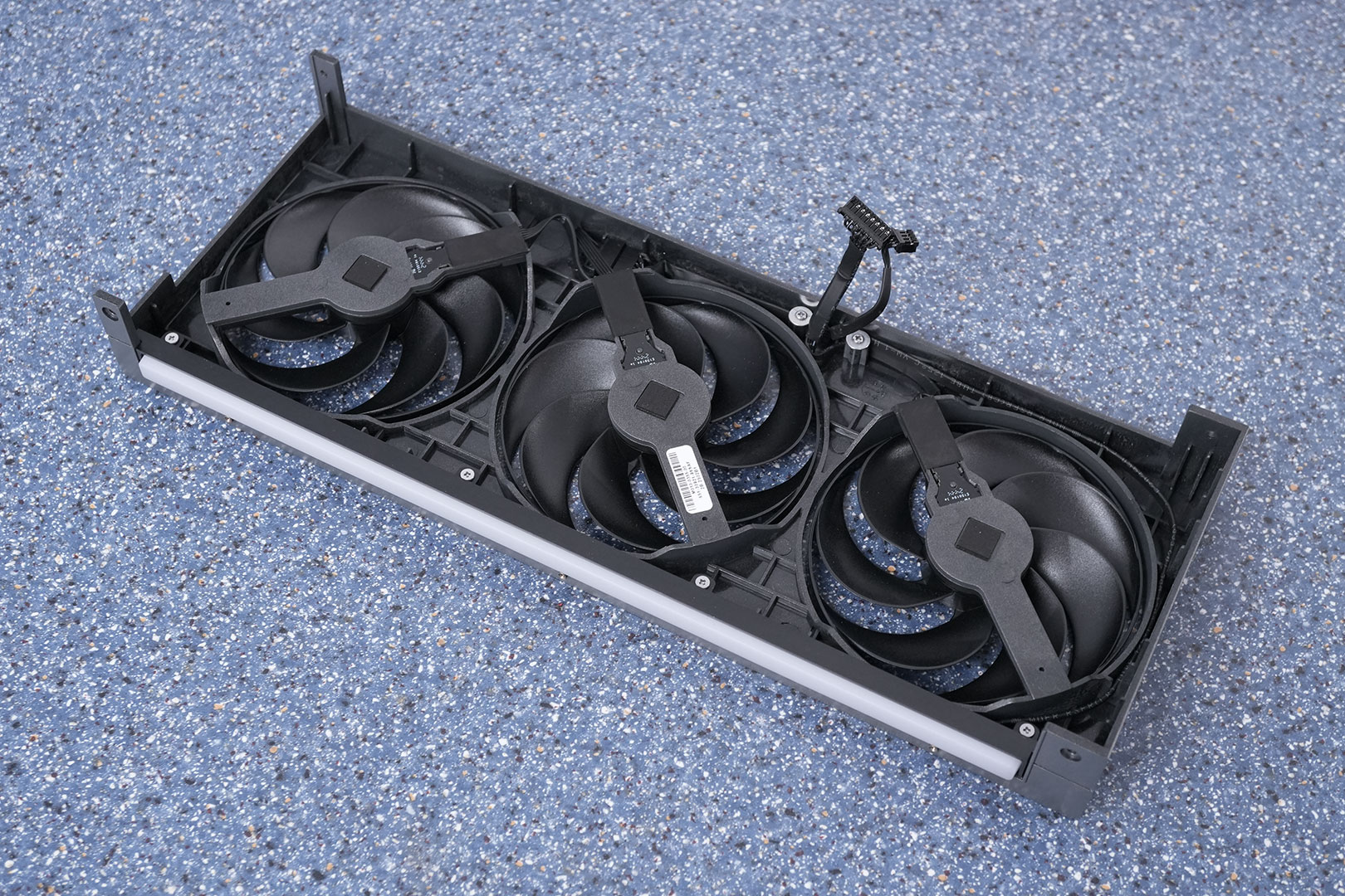
Sapphire made the fan assembly removable, without touching the thermal paste. This can come in handy if you have to replace one of the fans after a few years.
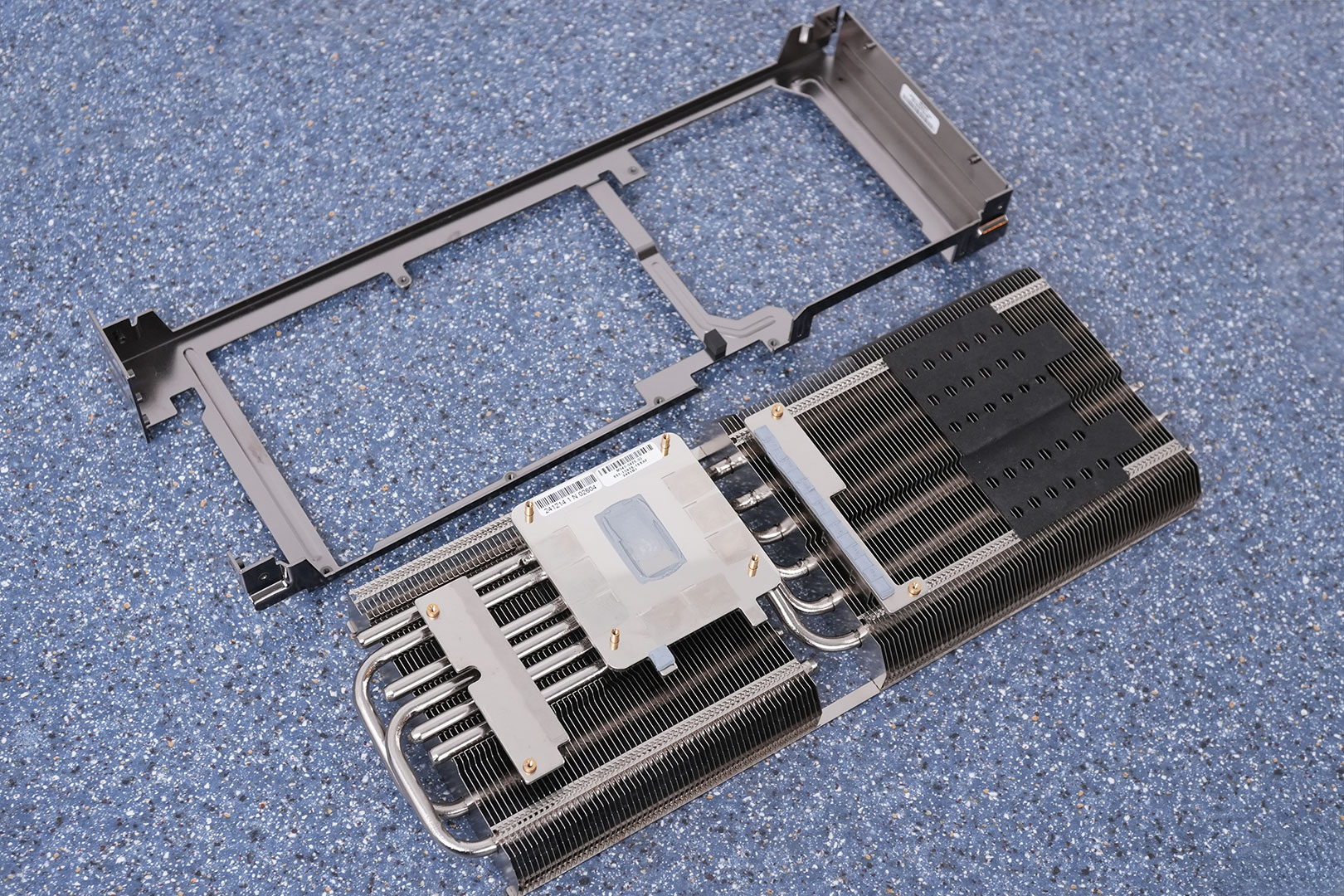
Under the main cooler a reinforcement frame has been placed.
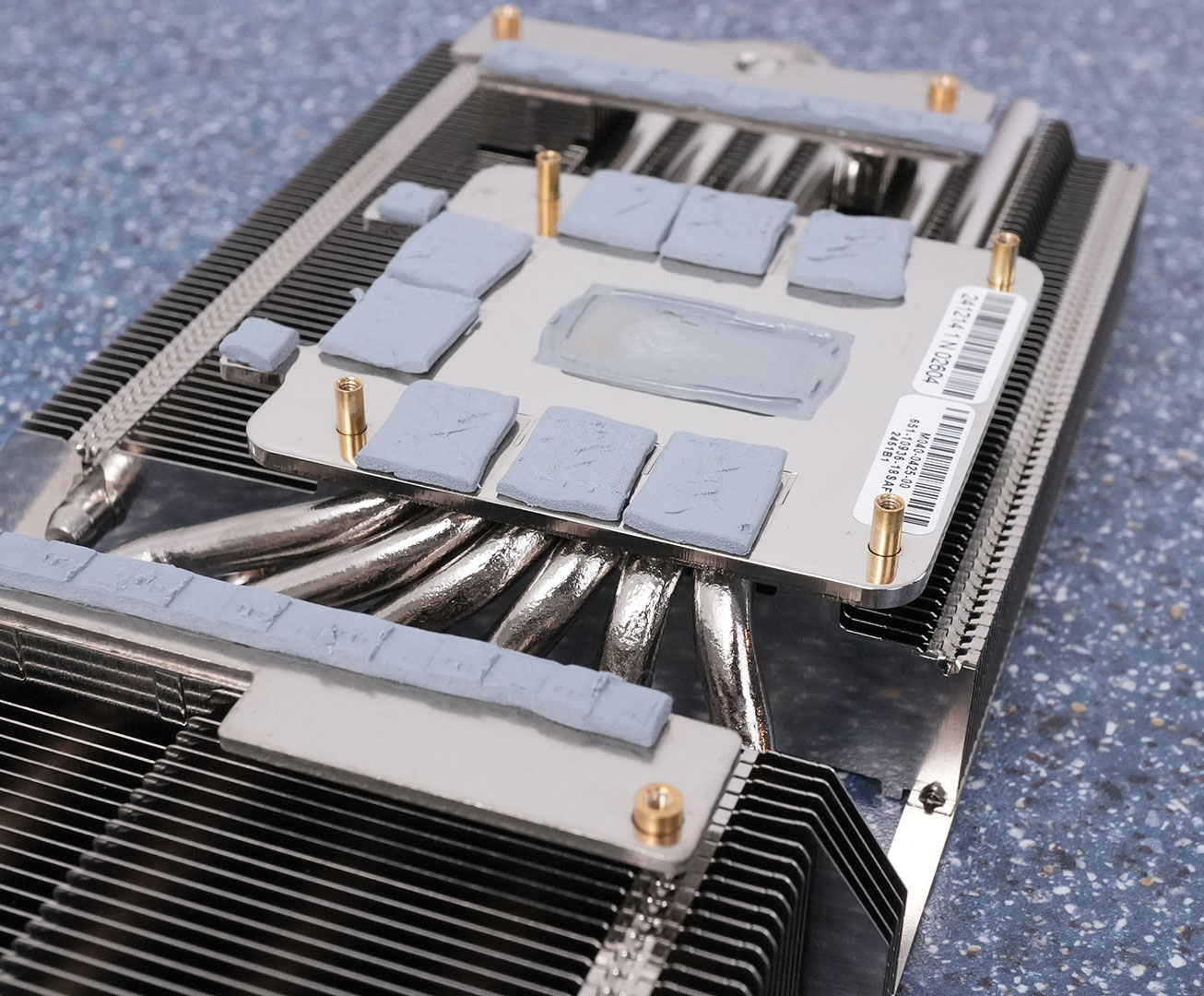
Sapphire's cooler uses six heatpipes. The heatsink provides cooling not only for the GPU, but also for the memory chips and VRM circuitry.
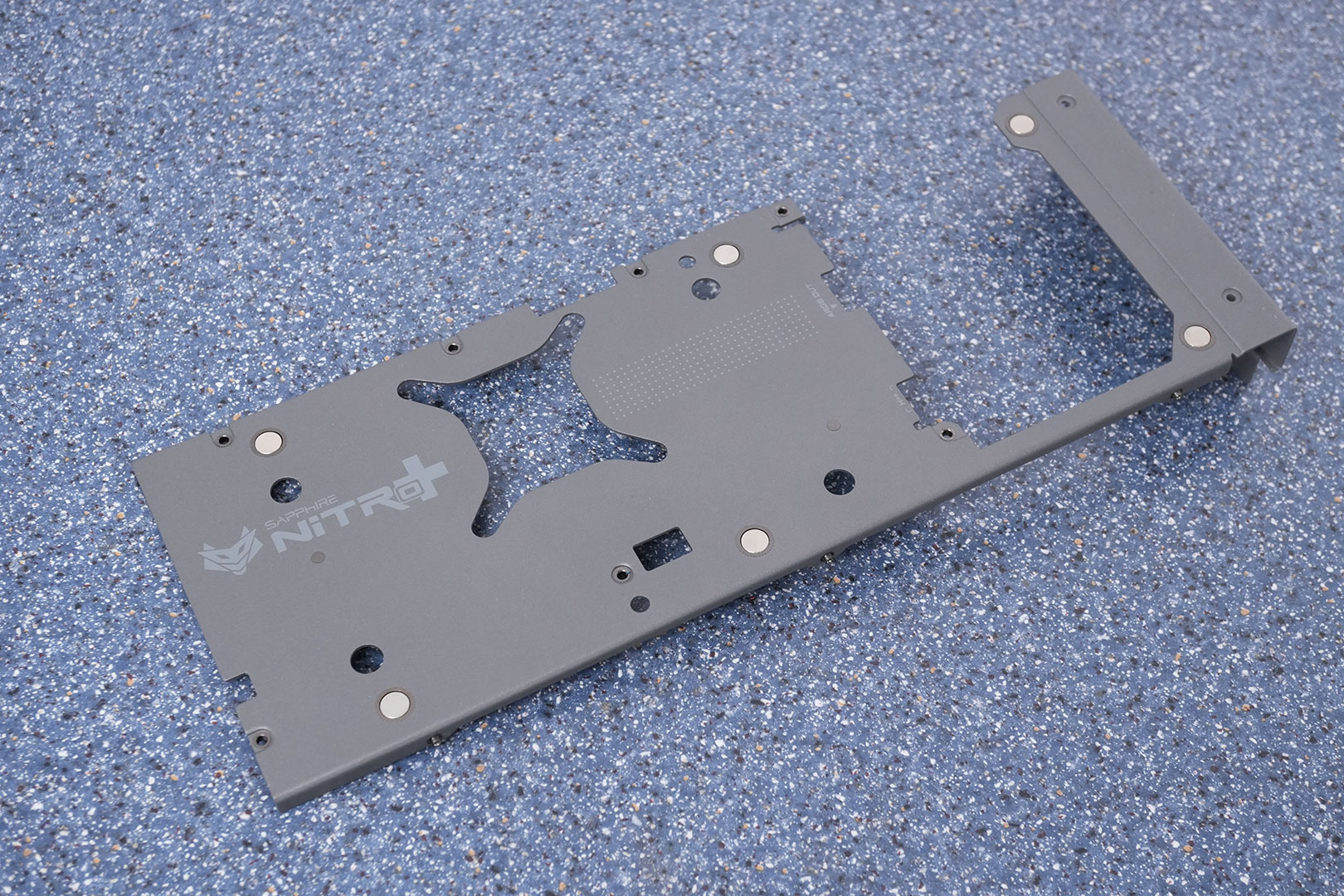
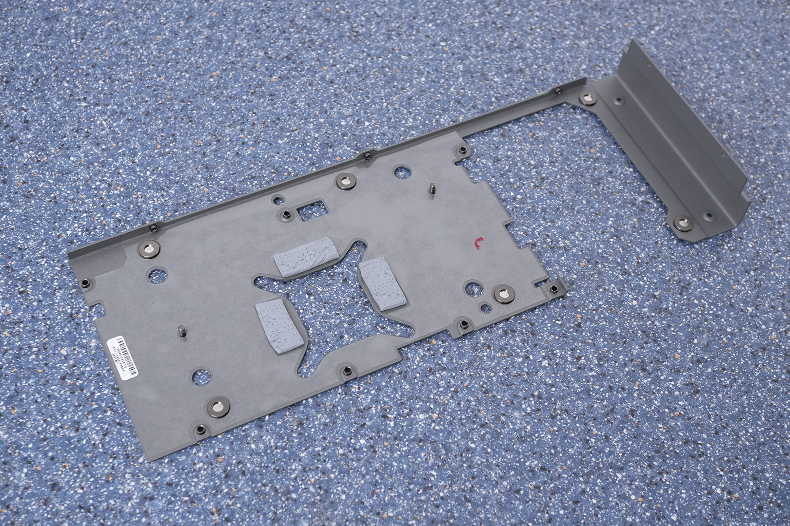
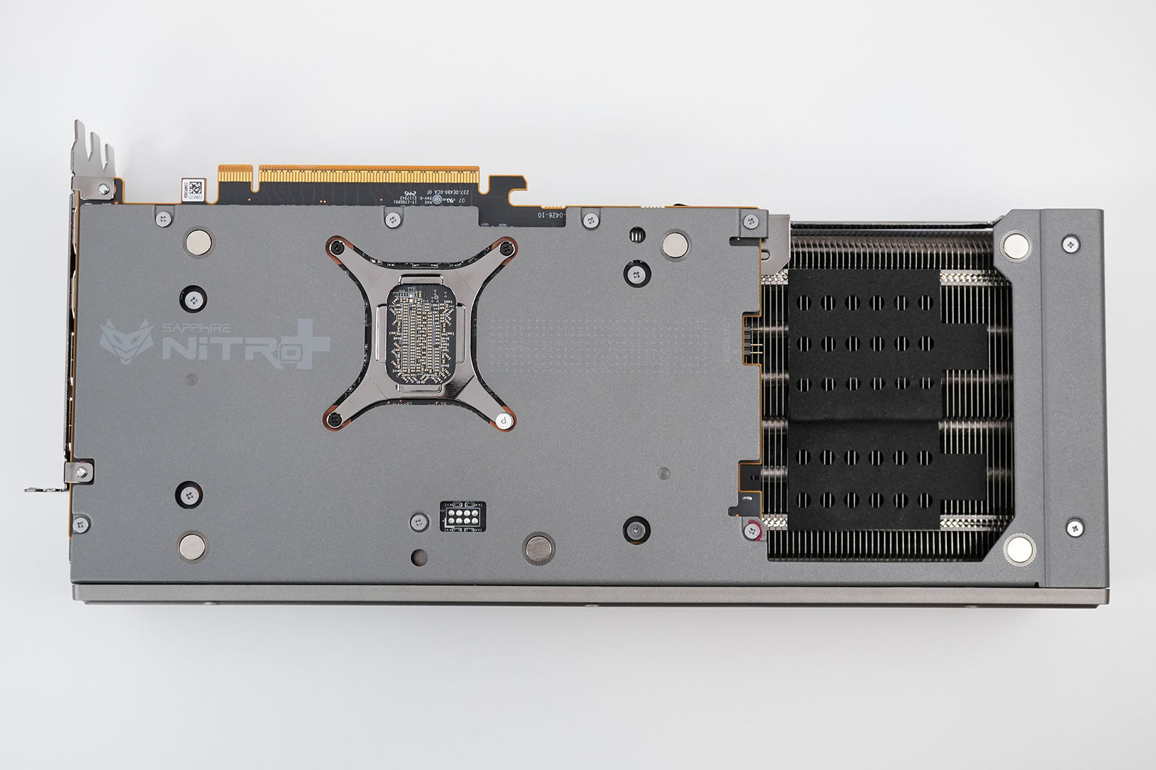
The backplate protects the PCB against damage during handling and installation.
High-resolution PCB Pictures
These pictures are for the convenience of volt modders and people who would like to see all the finer details on the PCB. Feel free to link back to us and use these in your articles, videos or forum posts.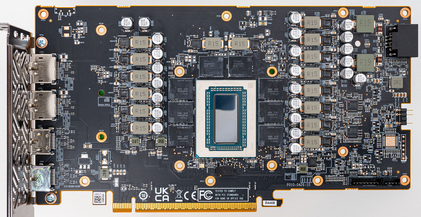
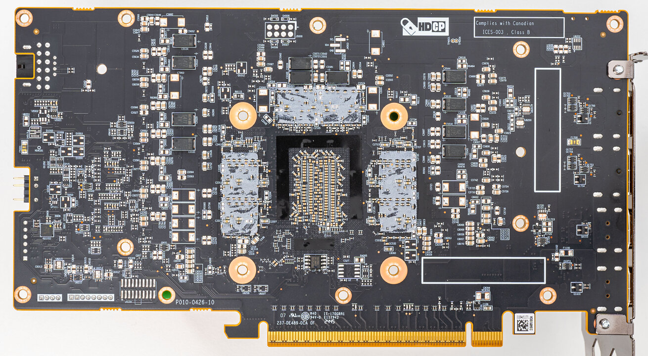
High-resolution versions are also available (front, back).
Our Patreon Silver Supporters can read articles in single-page format.
Mar 12th, 2025 21:12 EDT
change timezone
Latest GPU Drivers
New Forum Posts
- Warning message when unlocking PP0 Current Limit (2)
- 7950x3d vs 9900x3d for gaming (1)
- GameTechBench GPU benchmark is already out! (318)
- aios... don't leak from the fans.... right? (Fan is acculamating droplets) (2)
- Post your Old CDs & FDs, from back in the day thread. (68)
- RX 9070 availability (222)
- Zen6 is almost here ? (61)
- Bright Memory: Infinite Ray Tracing Benchmark (21)
- I'm looking for a good tool to make the 3D scanning of my mini-pc using the photogrammetry and my Kinect 2. (76)
- What motherboard with spdif should I get? PC to 5.1 blu-ray player via optical (7)
Popular Reviews
- AMD Ryzen 9 9950X3D Review - Great for Gaming and Productivity
- XFX Radeon RX 9070 XT Mercury OC Magnetic Air Review
- Sapphire Radeon RX 9070 XT Nitro+ Review - Beating NVIDIA
- Dough Spectrum Black 32 Review
- ASUS Radeon RX 9070 TUF OC Review
- FSP MP7 Black Review
- AMD Ryzen 7 9800X3D Review - The Best Gaming Processor
- NVIDIA GeForce RTX 5070 Founders Edition Review
- MSI MAG B850 Tomahawk Max Wi-Fi Review
- XPG Starker Air BTF Review
Controversial News Posts
- NVIDIA GeForce RTX 50 Cards Spotted with Missing ROPs, NVIDIA Confirms the Issue, Multiple Vendors Affected (513)
- AMD Radeon RX 9070 and 9070 XT Listed On Amazon - One Buyer Snags a Unit (261)
- AMD RDNA 4 and Radeon RX 9070 Series Unveiled: $549 & $599 (260)
- AMD Mentions Sub-$700 Pricing for Radeon RX 9070 GPU Series, Looks Like NV Minus $50 Again (249)
- NVIDIA Investigates GeForce RTX 50 Series "Blackwell" Black Screen and BSOD Issues (244)
- AMD Radeon RX 9070 and 9070 XT Official Performance Metrics Leaked, +42% 4K Performance Over Radeon RX 7900 GRE (195)
- AMD Radeon RX 9070-series Pricing Leaks Courtesy of MicroCenter (158)
- AMD Radeon RX 9070 XT Reportedly Outperforms RTX 5080 Through Undervolting (101)