 22
22
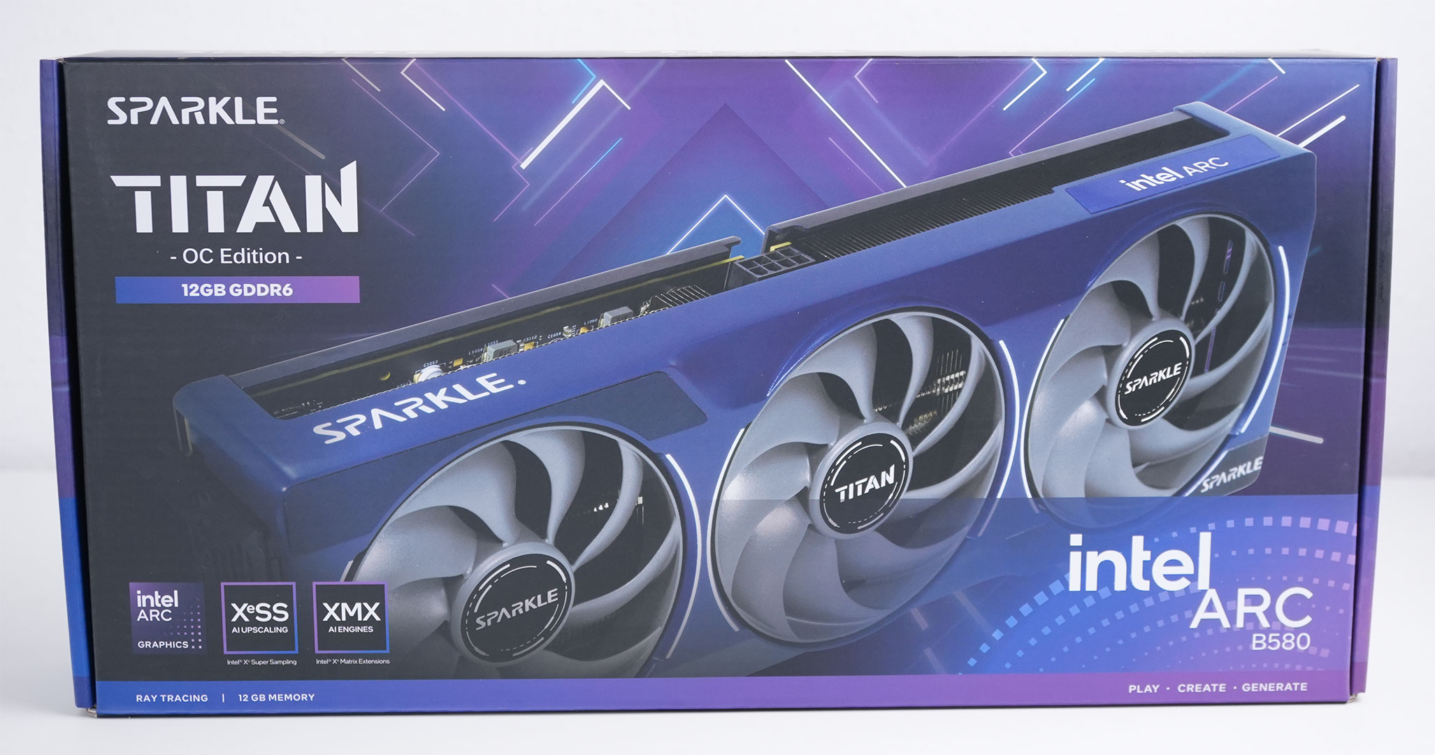
Sparkle Arc B580 Titan OC Review
(22 Comments) »Introduction
We have with us the Sparkle Arc B580 Titan OC graphics card, powered by the new B580 Battlemage GPU that's been making waves since its reveal earlier this month. Sparkle is a fairly new entrant to the Intel Arc graphics card ecosystem, but has been around for decades, notably as a former NVIDIA GeForce board partner. Now they are owned by TUL—the parent company of PowerColor. The Titan OC is the company's premium custom-design based on the B580, and pairs the GPU with a 31.5 cm-long triple-fan cooling solution that's a little over two slots thick. The Arc B580 marks Intel's second generation of the Xe gaming graphics architecture as discrete GPUs. These are modern, fulfill the DirectX 12 Ultimate API standards, and include a wide range of gaming experience improvements within the XeSS 2 feature suite.

Xe2 Battlemage succeeds the original Xe Alchemist. It debuted earlier this year as the architecture driving the iGPU of Intel's Core Ultra 200V Lunar Lake mobile processors, although that variant was a "lite" implementation of Xe2. On the Arc B580, you can expect a more complete set of the Xe2 Battlemage IP, with the GPU being geared for performance-segment gaming. The B580 logically succeeds the Arc A580, but presents a massive generational performance step-up. Intel claims (and we're confirmed in our review of the reference design), that the B580 outperforms every GPU from the Alchemist generation, including the top A770, and since the A770 was marketed as a 1440p-class GPU, this use case carries on for the B580.
In all, Intel claims a 70% gain in the SIMD performance of its 2nd Gen Xe cores over Alchemist, and a 50% gain in performance-per-watt, due in part to the new TSMC 5 nm EUV foundry node these chips are being built on. This is thanks to the significant IPC gain of the 2nd Gen Xe core, a new Ray Tracing Unit with anywhere between 50% to 100% generational gains in performance, a large 18 MB on-die last-level cache, and a faster memory sub-system than the A580, besides double the memory size, at 12 GB.
The B580 is being pitted by Intel against the NVIDIA GeForce RTX 4060. If you recall, the previous generation flagship parts, the A770 and A750, were compared by Intel to the RTX 3060, and the A580 was awkwardly positioned against the RTX 3050. In this sense, Intel has made a bigger generational leap in performance than NVIDIA, and we can only hope that Intel scales out the Xe2 architecture for even larger GPUs.
The Arc B580 is based on the 5 nm BMG-G21 silicon, and features 20 Xe cores, or 128 execution units, worth 2,560 unified shaders. There are also 20 Ray Tracing Units, and 160 XMX units, which accelerate AI. This is backed by a solid raster graphics backend, consisting of 80 ROPs, and 160 TMUs. The chip gets 12 GB of 19 Gbps GDDR6 memory across a 192-bit wide memory bus, which is both 50% larger and faster than the memory implementation of the RTX 4060 and the AMD Radeon RX 7600.
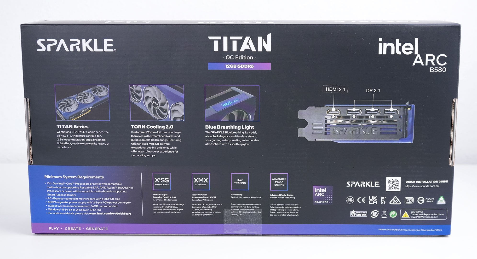
Perhaps the biggest aspect of the Arc B580 is its starting price of $250, which undercuts the RTX 4060 and the RX 7600 XT by at least $50. The Sparkle Arc B580 Titan OC looks like it's from a segment above, and yet, is being offered at just a $20 premium over this. The card is 31.5 cm in length and comes with a factory overclocked speed of 2740 MHz, compared to the 2670 MHz reference speed. It also comes with a slight increase in power limits to 200 W, from 190 W reference.
| Price | Cores | ROPs | Core Clock | Boost Clock | Memory Clock | GPU | Transistors | Memory | |
|---|---|---|---|---|---|---|---|---|---|
| RX 6500 XT | $140 | 1024 | 32 | 2685 MHz | 2825 MHz | 2248 MHz | Navi 24 | 5400M | 4 GB, GDDR6, 64-bit |
| Arc A580 | $180 | 3072 | 96 | 1700 MHz | N/A | 2000 MHz | ACM-G10 | 21700M | 8 GB, GDDR6, 256-bit |
| RTX 3050 | $165 | 2560 | 32 | 1552 MHz | 1777 MHz | 1750 MHz | GA106 | 12000M | 8 GB, GDDR6, 128-bit |
| Arc A750 | $220 | 3584 | 112 | 2050 MHz | N/A | 2000 MHz | ACM-G10 | 21700M | 8 GB, GDDR6, 256-bit |
| RX 6600 XT | $205 | 2048 | 64 | 2359 MHz | 2589 MHz | 2000 MHz | Navi 23 | 11060M | 8 GB, GDDR6, 128-bit |
| RTX 3060 | $220 | 3584 | 48 | 1320 MHz | 1777 MHz | 1875 MHz | GA106 | 12000M | 12 GB, GDDR6, 192-bit |
| RX 7600 | $250 | 2048 | 64 | 2250 MHz | 2625 MHz | 2250 MHz | Navi 33 | 13300M | 8 GB, GDDR6, 128-bit |
| RX 7600 XT | $310 | 2048 | 64 | 2470 MHz | 2755 MHz | 2250 MHz | Navi 33 | 13300M | 16 GB, GDDR6, 128-bit |
| RTX 4060 | $285 | 3072 | 48 | 1830 MHz | 2460 MHz | 2125 MHz | AD107 | 18900M | 8 GB, GDDR6, 128-bit |
| Arc A770 | $250 | 4096 | 128 | 2100 MHz | N/A | 2187 MHz | ACM-G10 | 21700M | 16 GB, GDDR6, 256-bit |
| Arc B580 | $250 | 2560 | 80 | 2670 MHz | N/A | 2375 MHz | BMG-G21 | 19600M | 12 GB, GDDR6, 192-bit |
| Sparkle Arc B580 Titan OC | $270 | 2560 | 80 | 2740 MHz | N/A | 2375 MHz | BMG-G21 | 19600M | 12 GB, GDDR6, 192-bit |
| RTX 3060 Ti | $300 | 4864 | 80 | 1410 MHz | 1665 MHz | 1750 MHz | GA104 | 17400M | 8 GB, GDDR6, 256-bit |
| RTX 4060 Ti | $380 | 4352 | 48 | 2310 MHz | 2535 MHz | 2250 MHz | AD106 | 22900M | 8 GB, GDDR6, 128-bit |
| RX 6700 XT | $350 | 2560 | 64 | 2424 MHz | 2581 MHz | 2000 MHz | Navi 22 | 17200M | 12 GB, GDDR6, 192-bit |
| RTX 3070 | $320 | 5888 | 96 | 1500 MHz | 1725 MHz | 1750 MHz | GA104 | 17400M | 8 GB, GDDR6, 256-bit |
| RTX 3070 Ti | $370 | 6144 | 96 | 1575 MHz | 1770 MHz | 1188 MHz | GA104 | 17400M | 8 GB, GDDR6X, 256-bit |
| RX 6800 | $340 | 3840 | 96 | 1815 MHz | 2105 MHz | 2000 MHz | Navi 21 | 26800M | 16 GB, GDDR6, 256-bit |
| RX 7700 XT | $370 | 3456 | 96 | 2171 MHz | 2544 MHz | 2250 MHz | Navi 32 | 26500M | 12 GB, GDDR6, 192-bit |
| RX 6800 XT | $400 | 4608 | 128 | 2015 MHz | 2250 MHz | 2000 MHz | Navi 21 | 26800M | 16 GB, GDDR6, 256-bit |
Xe2 Battlemage Architecture
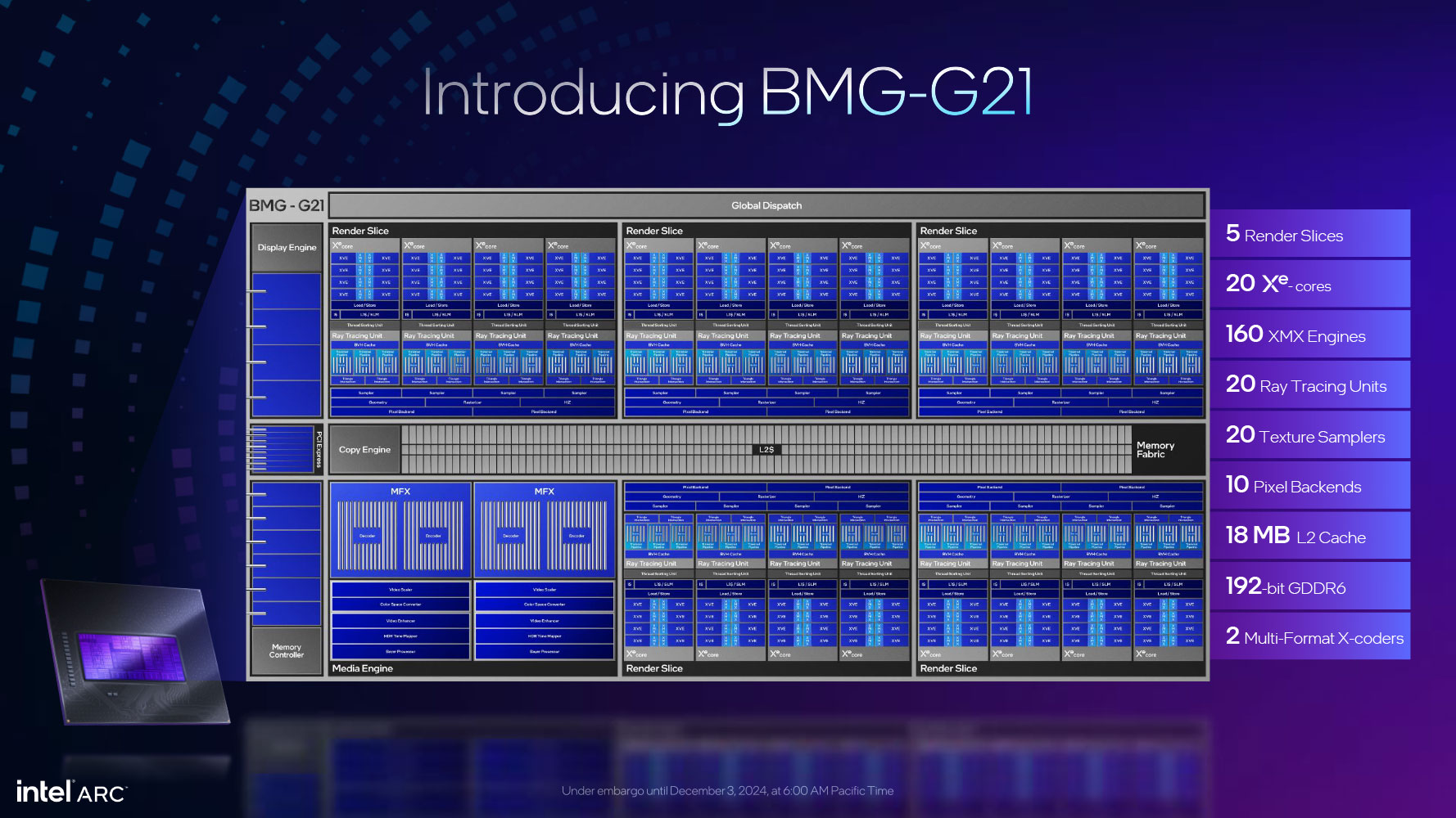
The Arc B580 debuts Intel's second discrete gaming GPU architecture, codenamed Xe2 "Battlemage." A variant of Xe2 is used in the integrated graphics solution of Intel's Core Ultra 200V "Lunar Lake" mobile processors, the one today is its fully-fledged discrete gaming GPU version, with all hardware components enabled. The Arc B580 is a mid-range model based on the BMG-G21 silicon. The B580 likely does not max-out the silicon, since it is meant to succeed the mid-range A580 "Alchemist." We asked, but Intel would not comment on future products. The BMG-G21 is built on the TSMC N5 (5 nm EUV) foundry node, and packs 19.6 billion transistors across a 272 mm² monolithic die. The 5 nm node is contemporary, given that both NVIDIA "Ada" and AMD RDNA 3 gaming GPUs use it.
The BMG-G21 GPU features a PCI-Express 4.0 x8 host interface on the Arc B580 and B570. It is configured with a 192-bit GDDR6 memory bus on the B580, and a 160-bit bus on the B570. The GPU is organized in a very similar manner to modern GPUs from NVIDIA and AMD—a Global Dispatch processor distributes work among the five Render Slices, which talk to each other over the GPU's fabric and memory sub-system. The GPU's internal last-level cache is 18 MB in size. Besides the five Render Slices, there is the Media Engine, consisting of two MFX (multi-format x-coders (encoders/decoders); there are two sets of hardware encoders and decoders. Then there's the GDDR6 memory controller and the Display Engine, with four display interfaces.
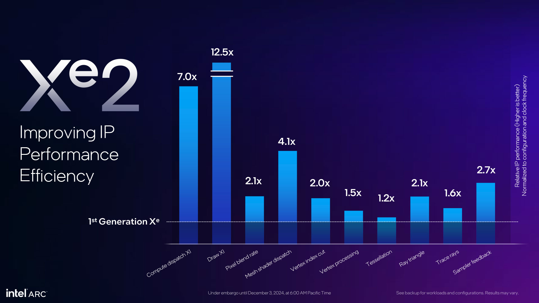
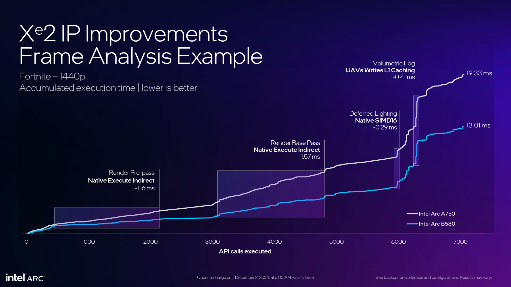
Intel is claiming a 70% generational increase in performance per Xe Core, the indivisible number-crunching subunit of the GPU; and a 50% generational performance-per-watt increase. The above graphs illustrate the contribution of the individual sub-systems of the Xe2 Battlemage architecture toward these improvements; and how this plays out in a frametime analysis example of a real-world use case.
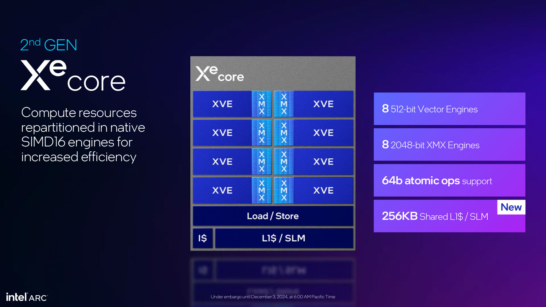
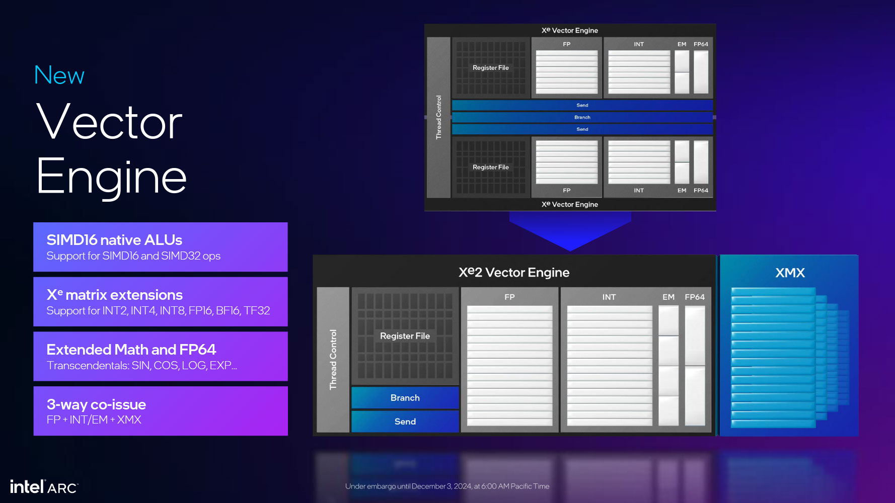
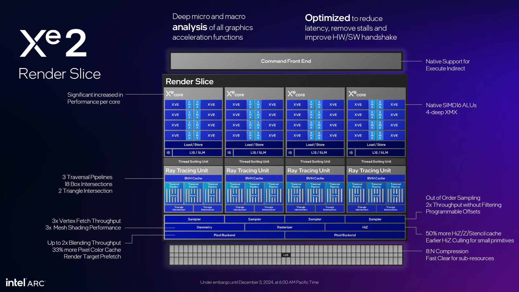
The Render Slice diagram (above) highlights the biggest chunk of the generational performance increase by Intel. It's thanks to increased IPC from the Xe Core, a more specialized and capable Ray Tracing Unit, a 300% faster Geometry engine, faster Sampler, 50% increase in HiZ, Z, stencil caches, and increases in performance of the pixel backends. Intel's engineering goal has been to reduce latency wherever it can, and reduce software (CPU) overhead as much as it can. The new 2nd Gen Xe Core features eight 512-bit vector engines, with SIMD16-native ALUs, and many more data formats. Rather than two sets of FP and INT units per vector engine, there is just one set of each per vector engine in Xe2, with larger numbers of ALUs.
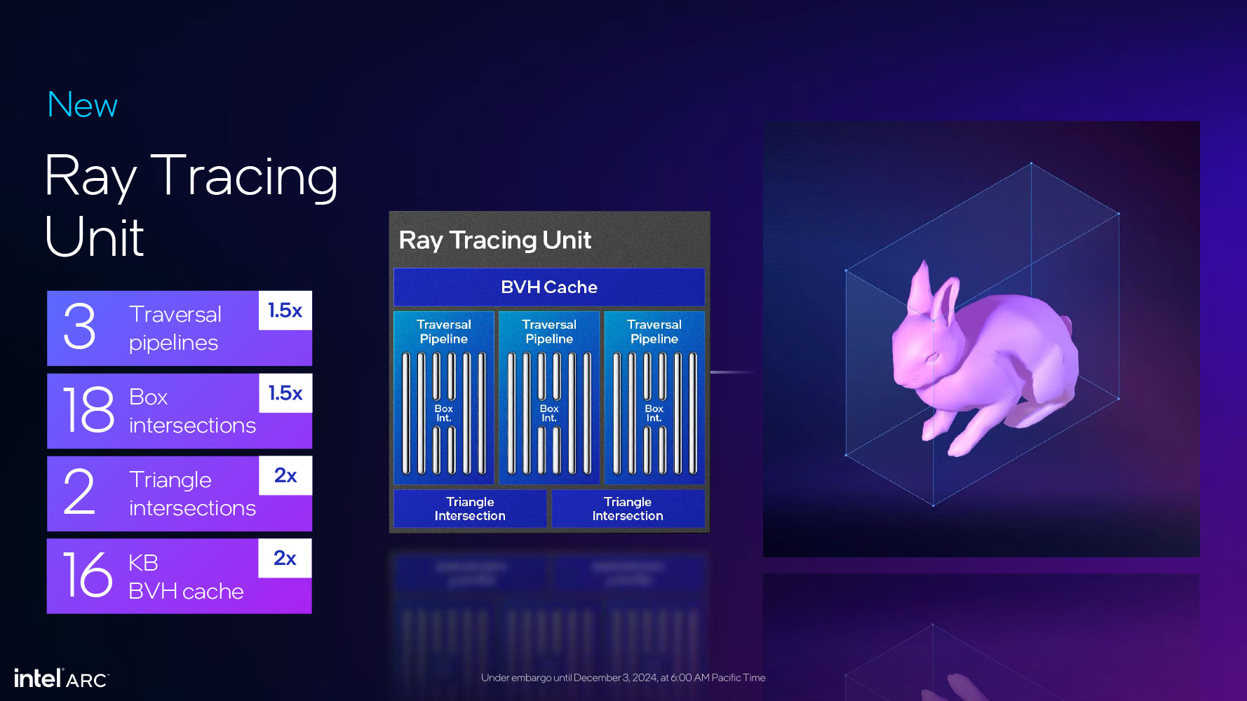
Intel introduced its second gen Ray Tracing Unit, with massive generational improvements in performance and capability. It introduces a third Traversal Pipeline, which yields a 50% increase in box intersection performance. A second triangle intersection unit has been added to double the performance of triangle intersections. The BVH cache has doubled in size to 16 KB.
XeSS 2, Frame Generation, and Low Latency
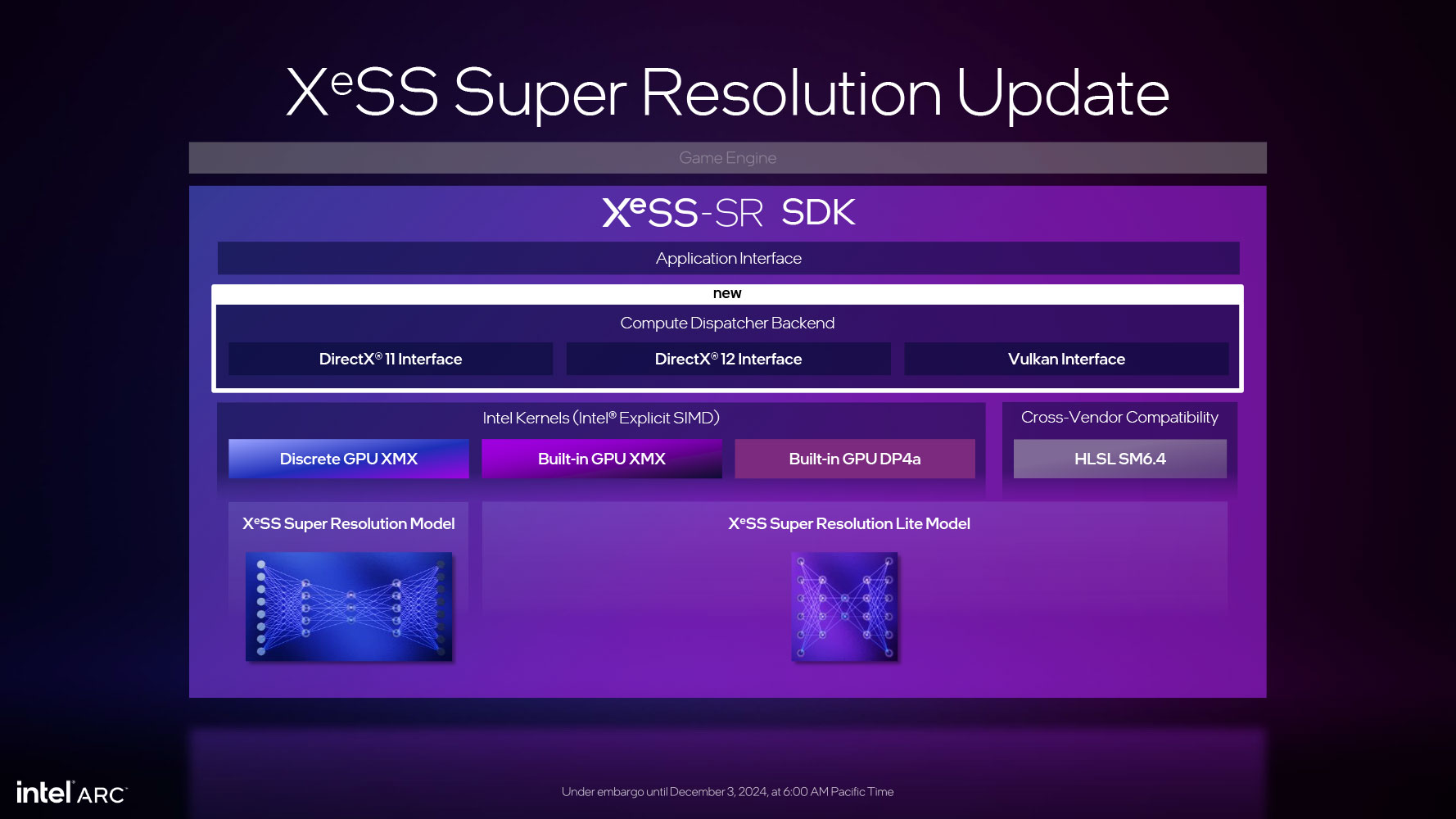
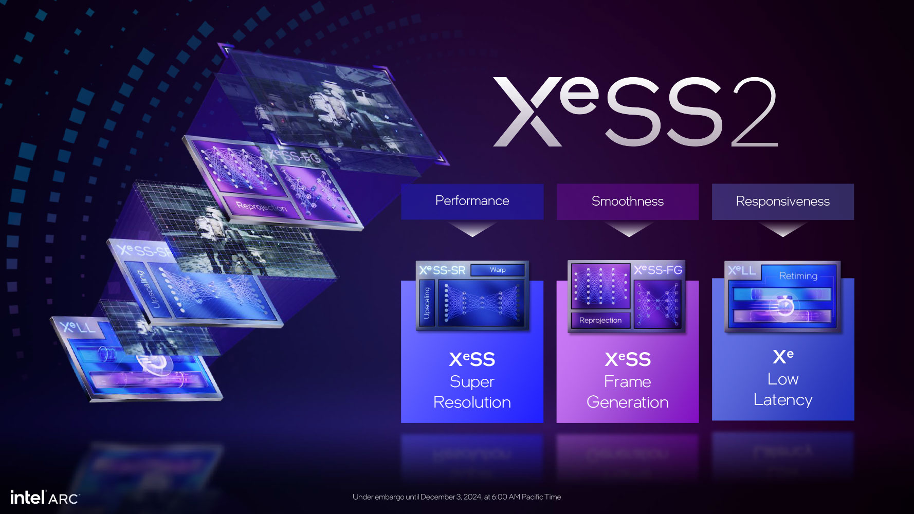
Intel has codified the original XeSS as XeSS Super Resolution (XeSS-SR), as that's what it originally was—a performance enhancement that relies on super-resolution technology. The XeSS-SR SDK gets a new compute dispatcher backend for popular APIs—DirectX 11, DirectX 12, and Vulkan. There are two XeSS-SR models, the regular one, and a XeSS-SR Lite model for GPUs that lack XMX matrix acceleration capability.
XeSS 2 isn't a single technology, or an improvement over XeSS-SR, but a collection of three technologies—the existing XeSS-SR, which deals with performance; the new XeSS Frame Generation (XeSS-FG) technology, which nearly doubles frame rates based on intelligent frame doubling; and the new Xe Low Latency (XeLL) technology, which works to reduce the latency cost of SR and FG, but is something that can be used as a standalone whole-system latency technology, too.
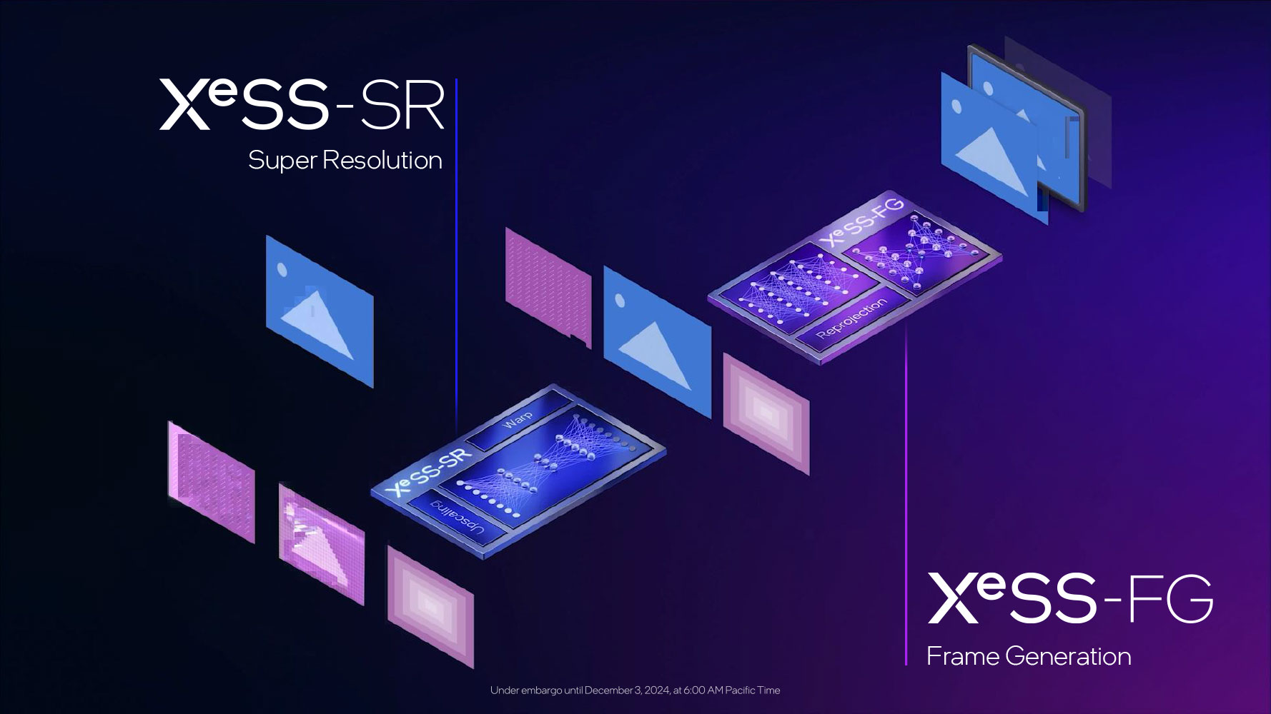
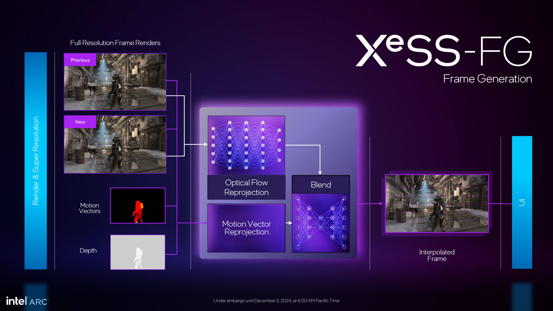
XeSS-FG can either be implemented at native resolution, or in conjunction with XeSS-SR, where it is located right after the XeSS-SR step in the rendering queue. It relies on motion vectors, depth data, temporal frame data, and optical flow reprojection, to create interpolated frames that are then interleaved with the output frames, to effectively double the framerate. The interpolated image is then passed along to the next stage, where the HUD/UI is added at native resolution, and pushed to the frame buffer for output.
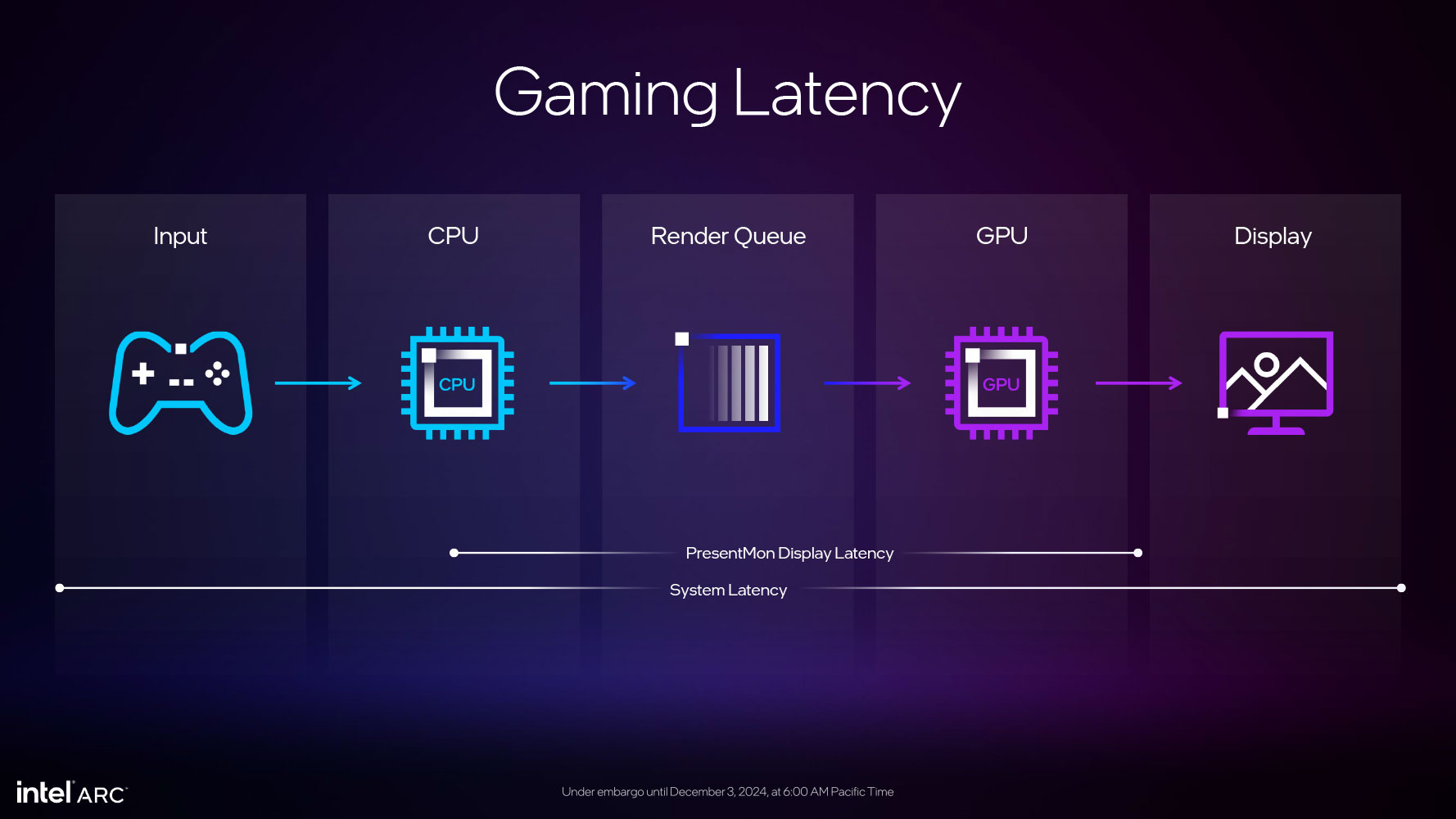
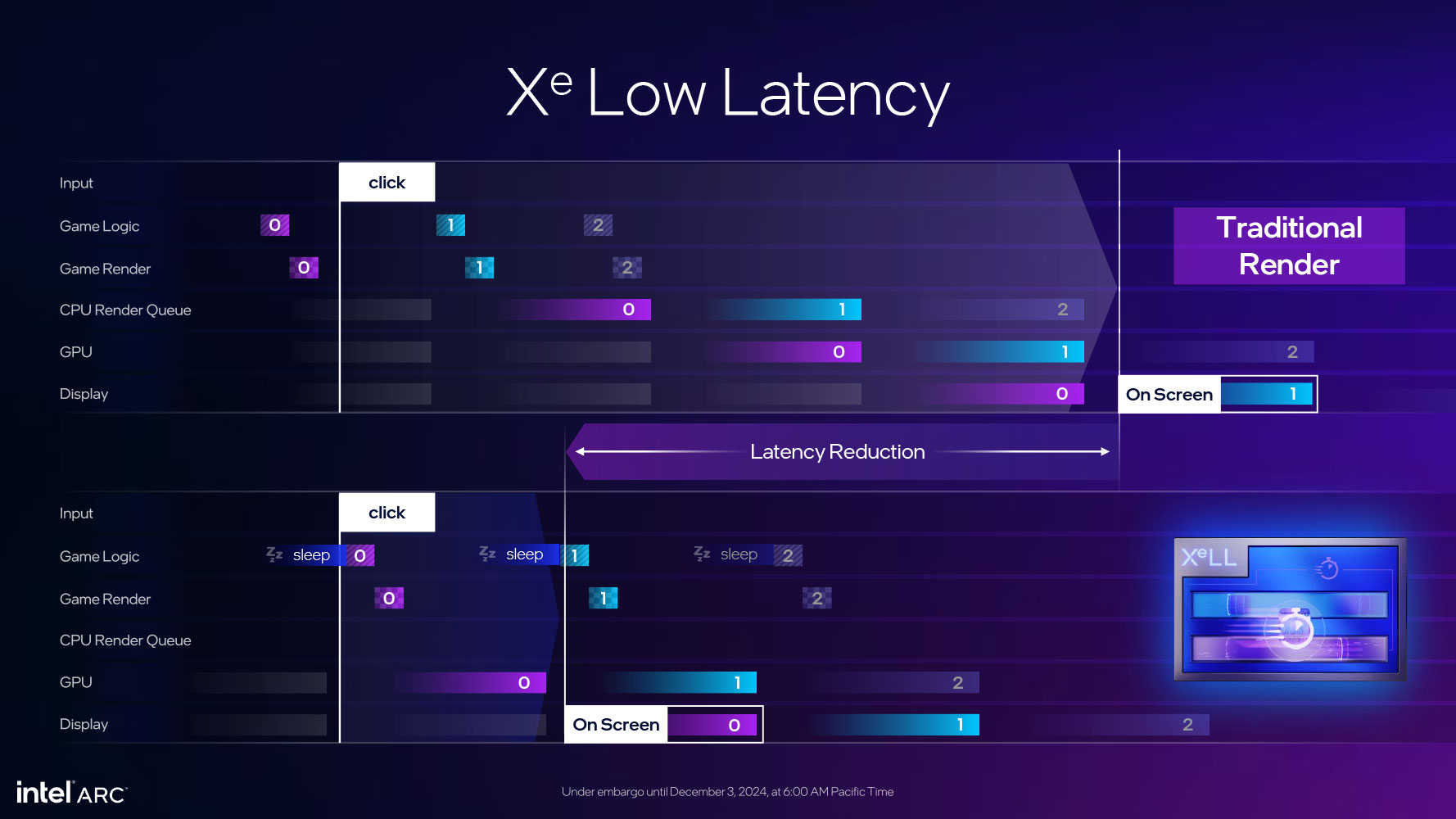
The SR + FG passes contribute to frame latency, and so, just as NVIDIA uses Reflex to counteract this latency, Intel innovated XeLL. The technology intelligently compacts the rendering queue to reduce the time it takes for an input to register as motion on-screen. XeLL remains enabled in all workloads the use XeSS-FG, but it can be used as a standalone feature, too. There's also an implicit driver-based low-latency mode that does this without a game having an explicit XeSS 2 or XeLL implementation.
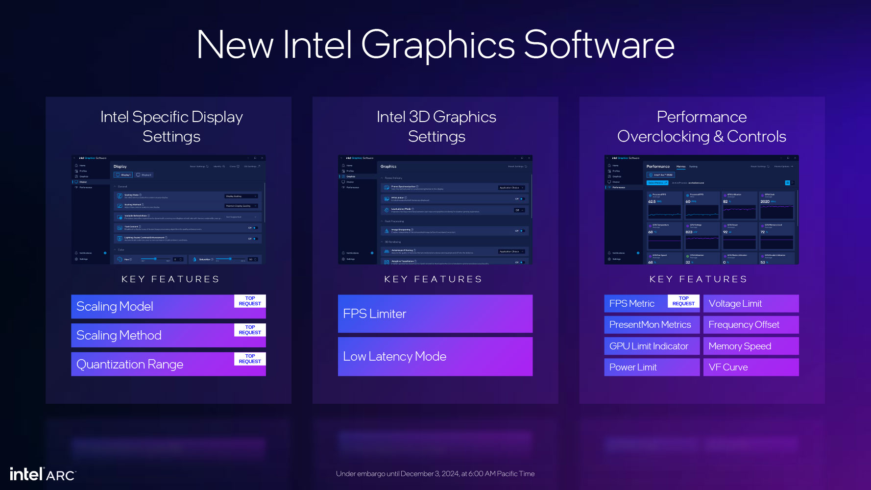
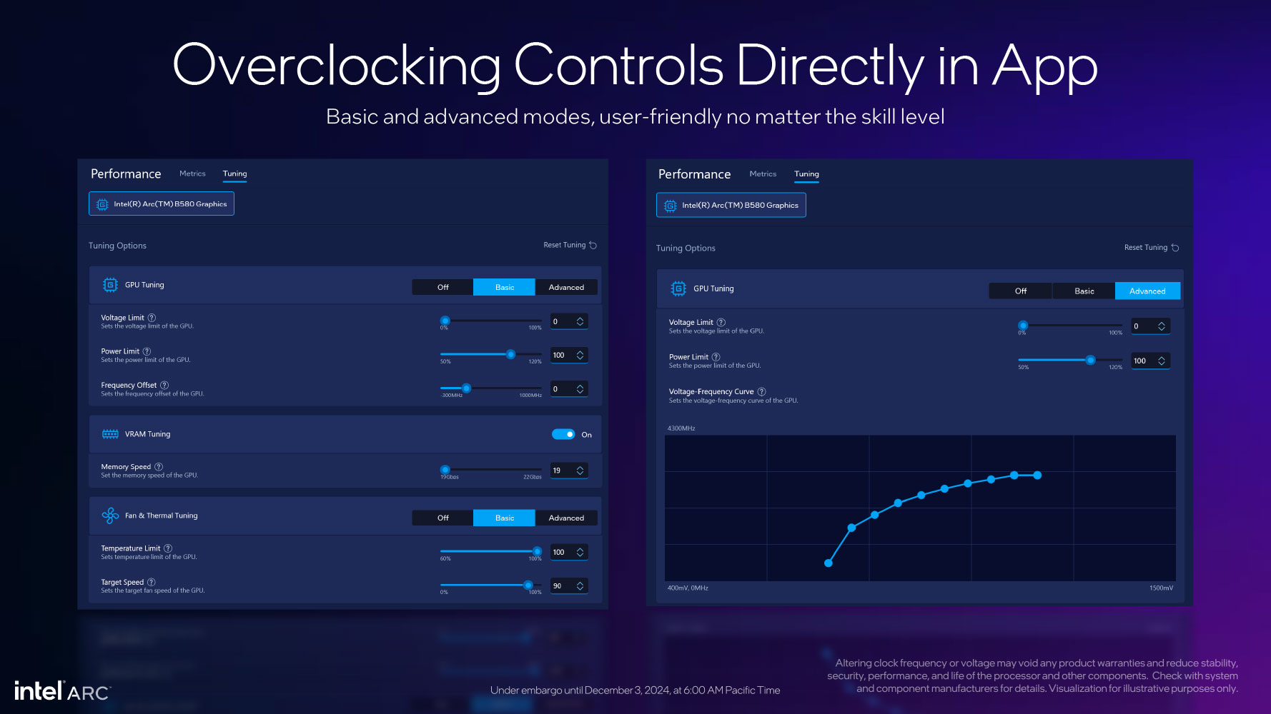
Intel has updated its software package significantly. The new "Intel Graphics Software" replaces the "Arc Control" utility, and gives you a cleaner user interface. There are many new settings related to the display, including display scaling model/method/quantization range; 3D graphics settings, including a driver-based FPS limiter, the driver-based low-latency mode; and the exhaustive new Performance and Overclocking controls, which include the ability to set frequency offsets, tinker with the V/F curve, power limits, and GPU and memory clocks. It also integrates Intel's PresentMon metrics.
Packaging
The Card
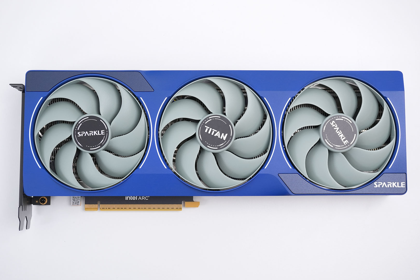
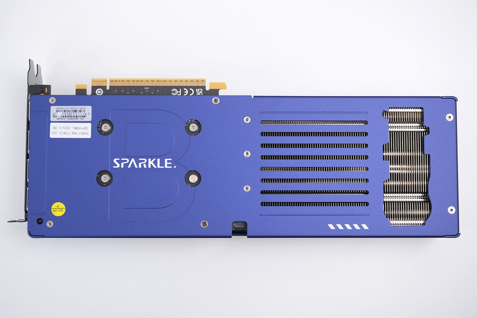
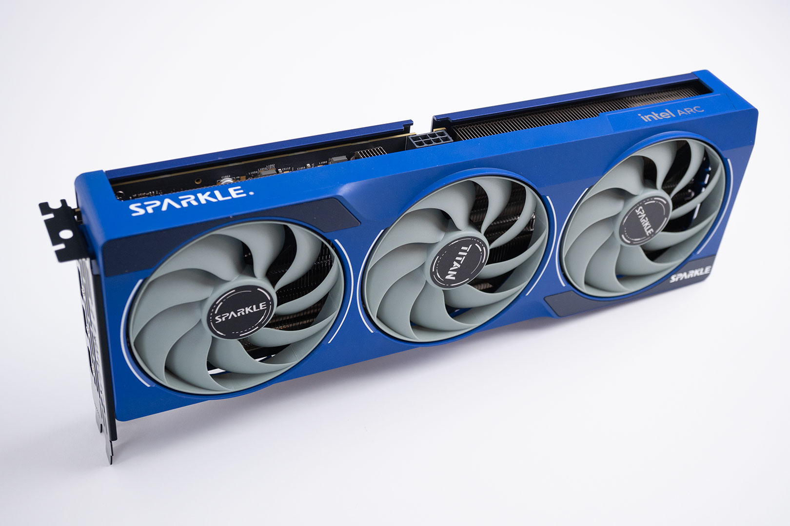
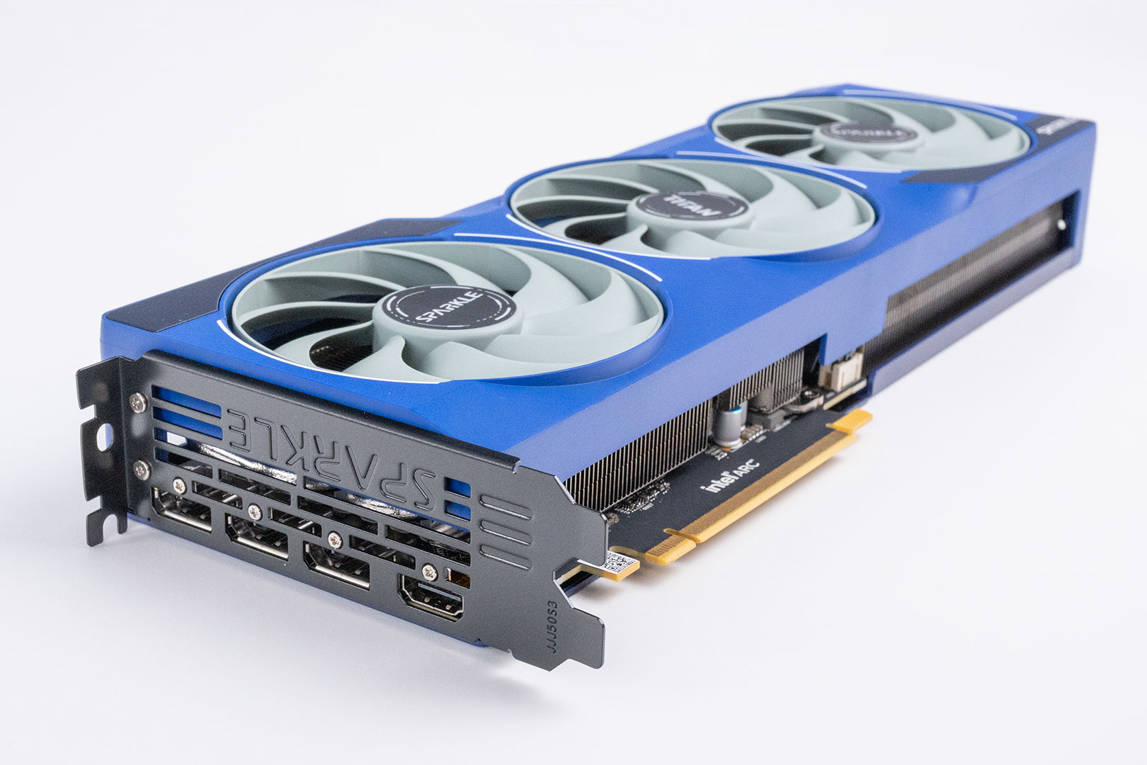
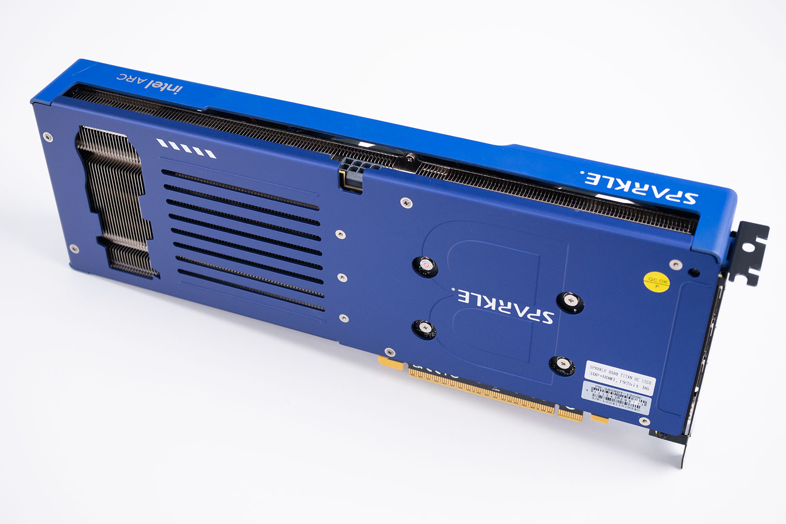
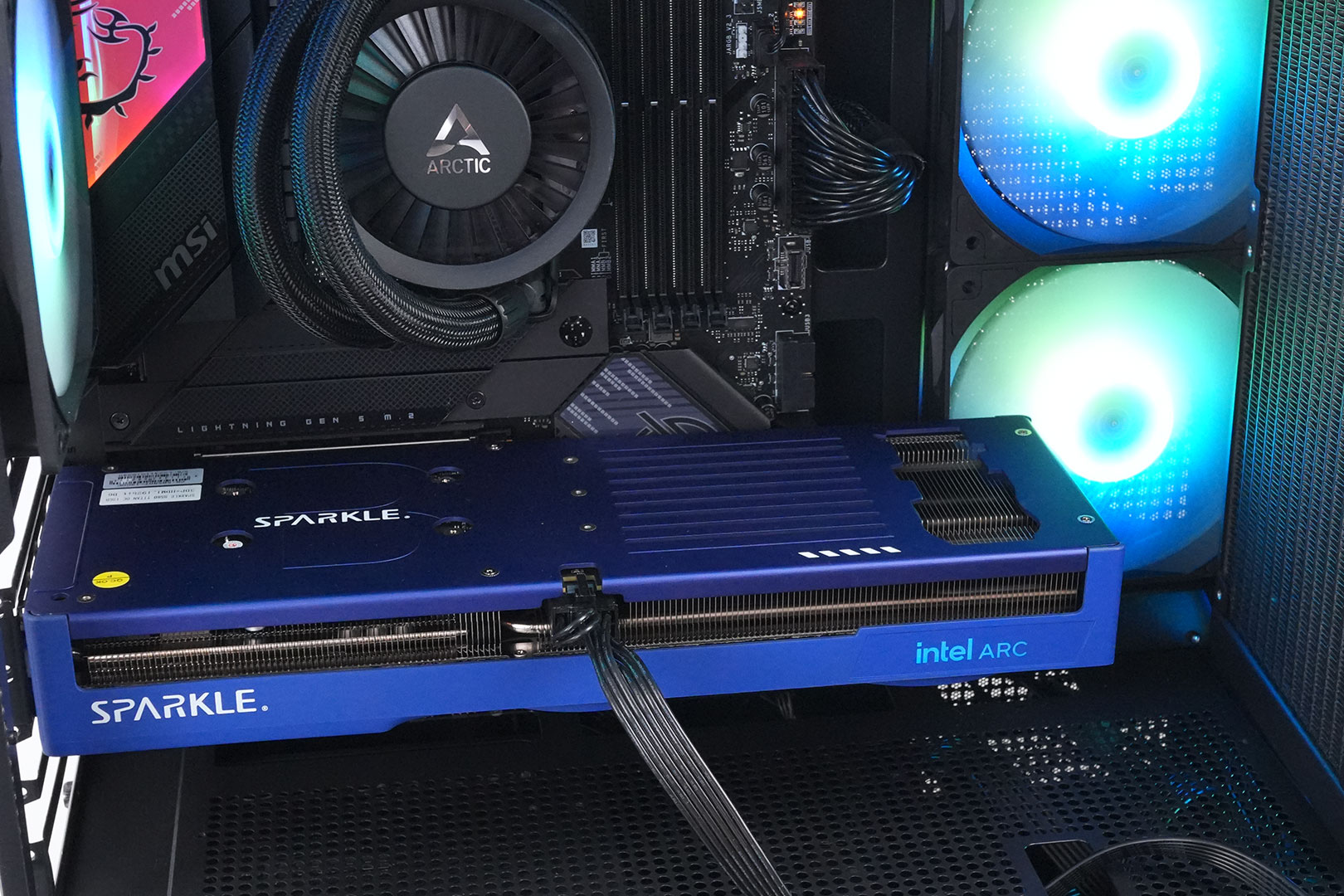
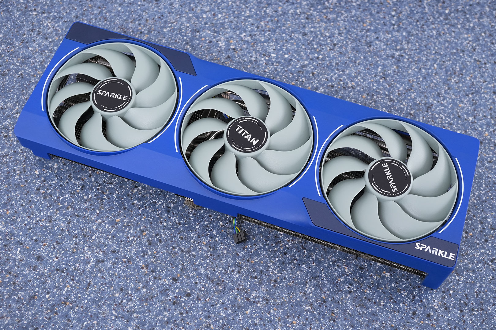
Sparkle's B580 Titan OC comes with a fantastic-looking blue color theme—I really love how the various shades of blue come together. On the back you get a high-quality metal backplate with a cutout for air to flow through.
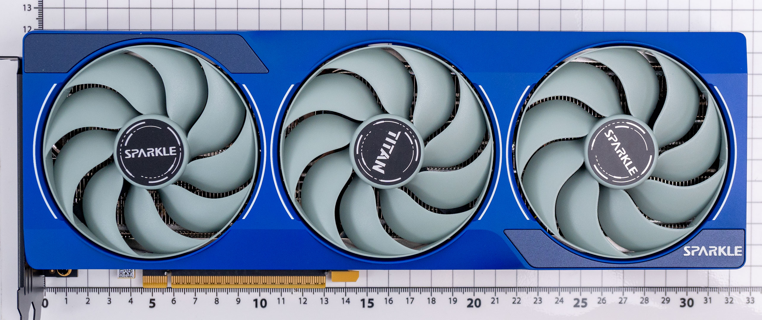
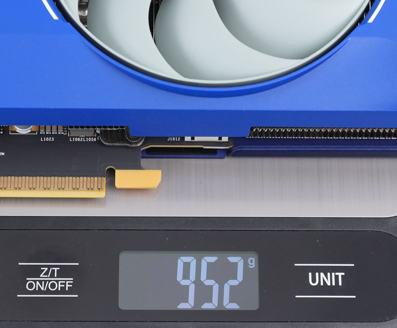
Dimensions of the card are 31.5 x 12.0 cm, and it weighs 952 g.
Installation requires two slots in your system. We measured the card's width to be 45 mm.
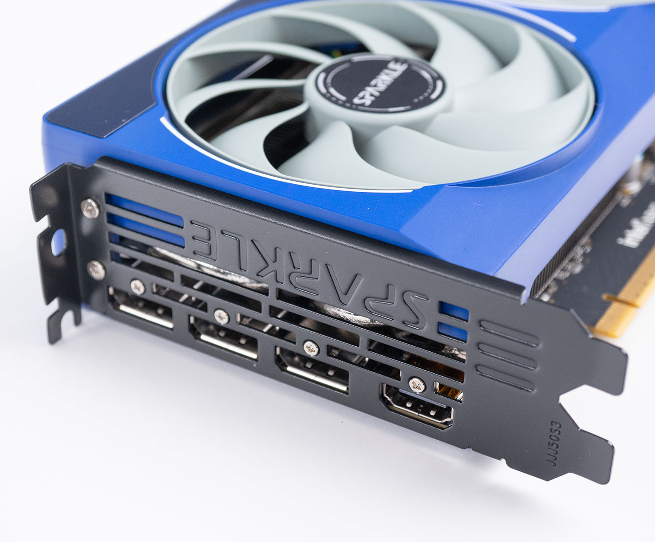
Display connectivity includes three standard DisplayPort 2.1 and one HDMI 2.1a. On the Intel reference card one port is marked with a black outline, but not on this card. That port supports higher bitrates (UHBR13.5), i.e. 4K up to 360 Hz, while the other two ports support up to 240 Hz, so I guess you have to test them to find the right one (if you have a monitor that requires such high transfer rates).
In terms of codecs, you get full support for H.264, H.265, VP9 and AV1, both encode and decode. Worth highlighting is HEVC 4:2:2 10-bit encoding and decoding, which is a unique capability, and AV1 Screen Content encoding, which improves the quality of text in movies—fantastic for screen recordings or screen sharing.
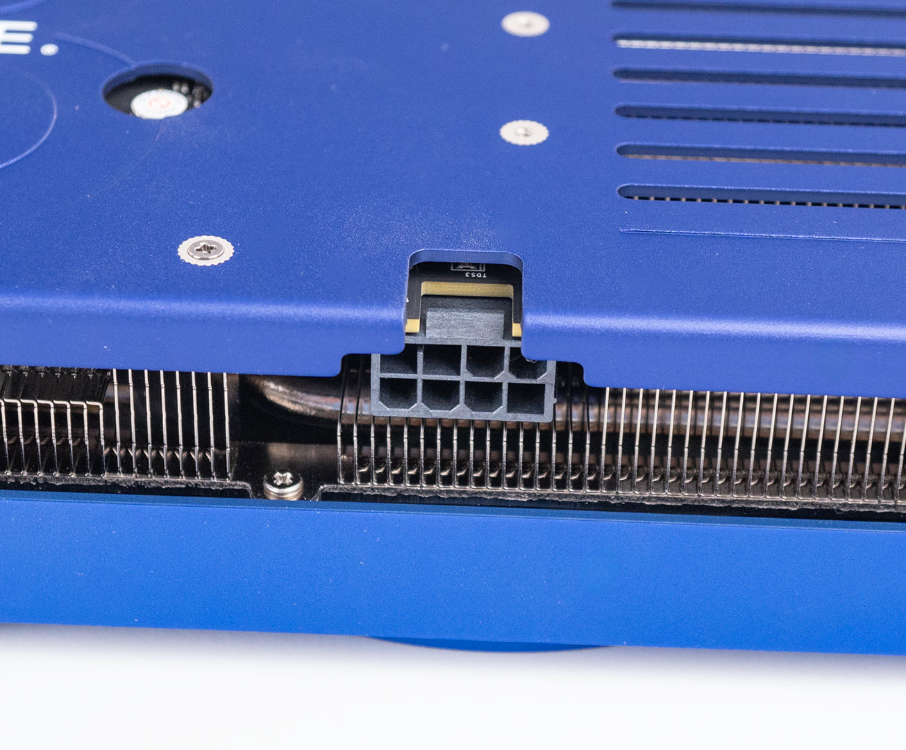
The card uses a single 8-pin connector, plus PCIe slot power, allowing a maximum power draw of 225 W. Sparkle has set their power limit to 200 W, 10 W higher than Intel default.
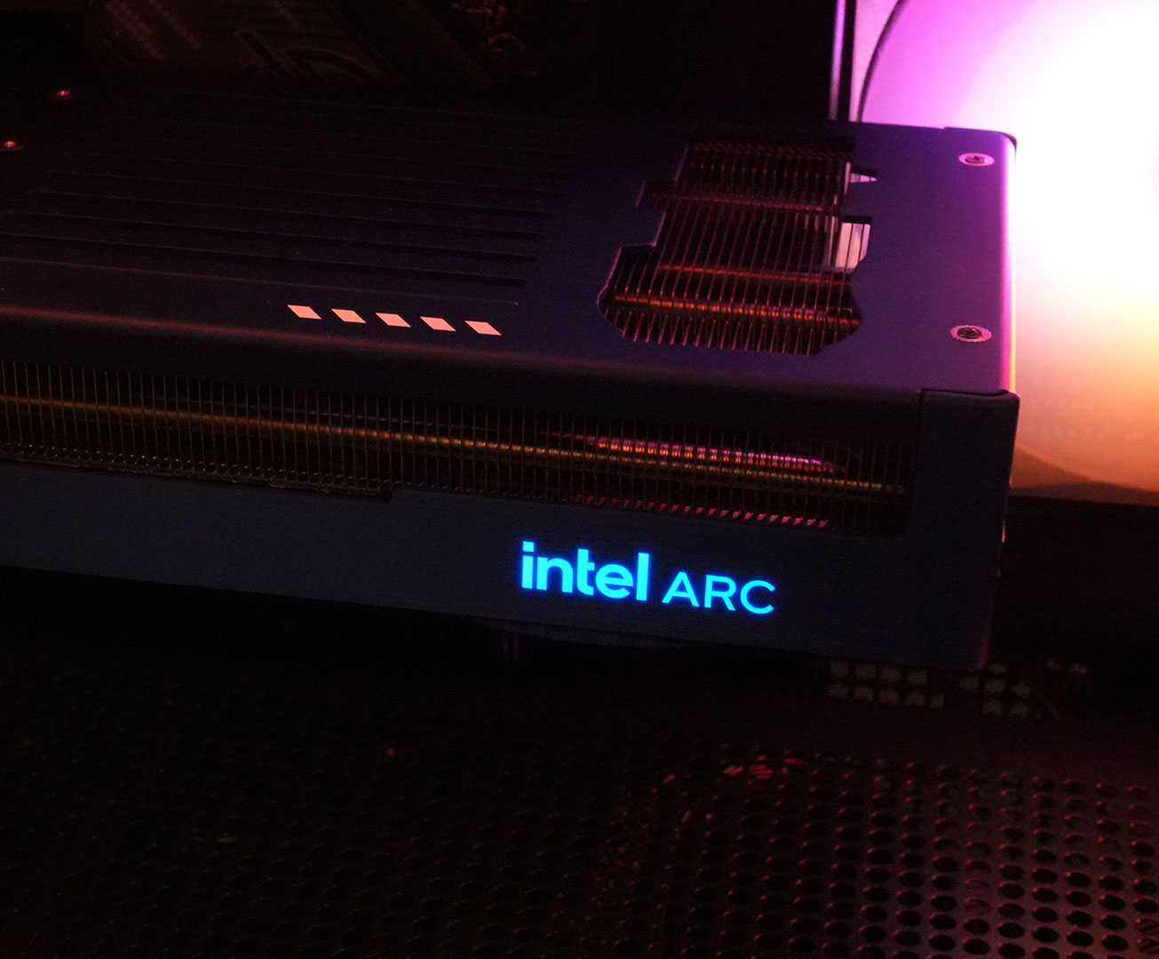
The card comes with an illuminated Intel ARC logo that's glowing blue and can't be controlled.
Teardown
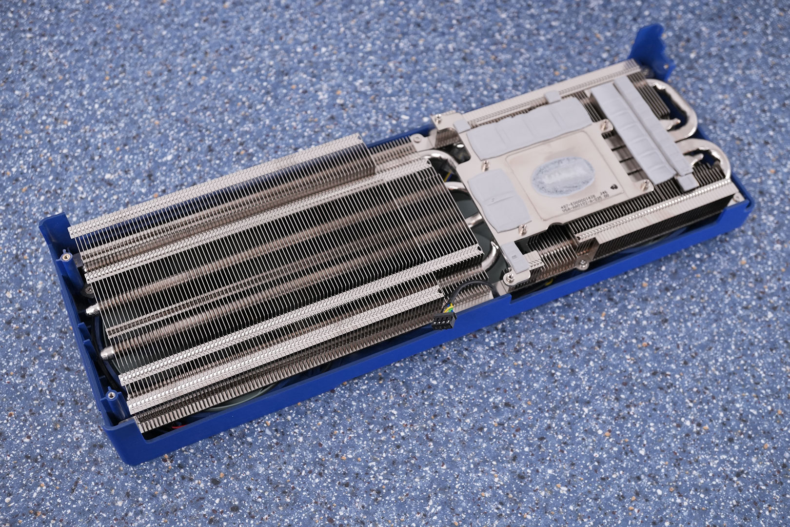
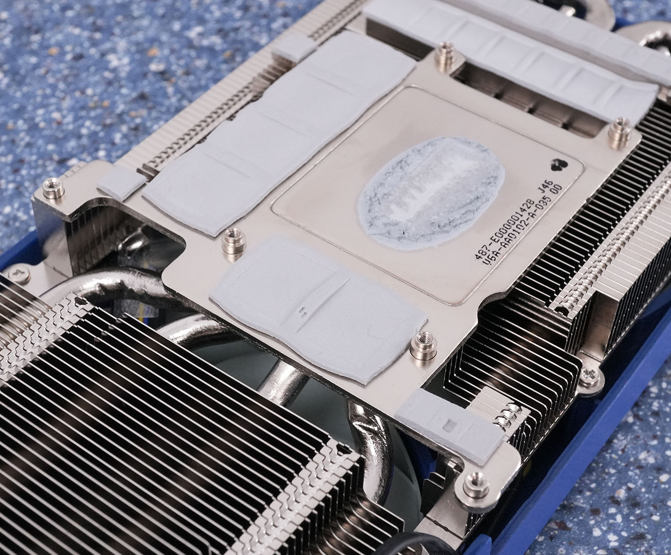
The main cooler uses four heatpipes and provides cooling for the GPU, memory and VRM circuitry.
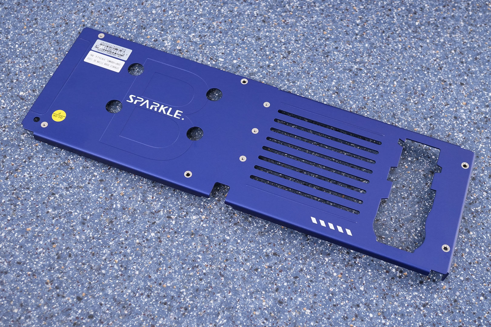
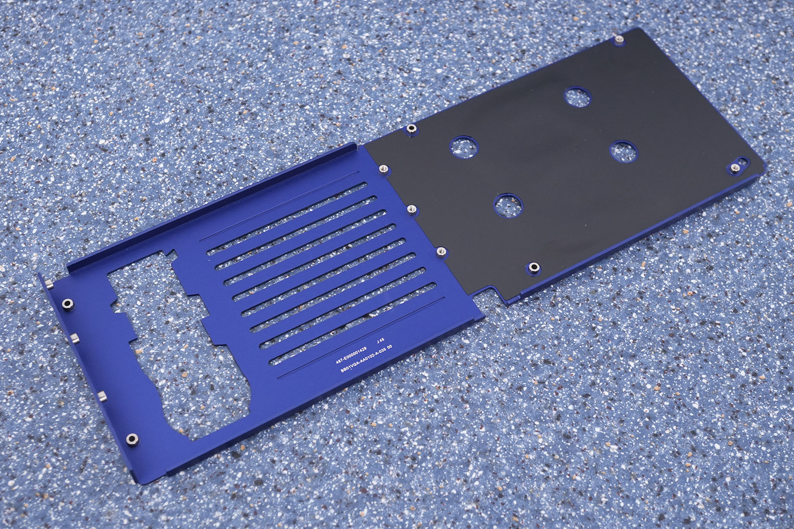
On the back, you'll find a metal backplate with cutouts to improve airflow.
Our Patreon Silver Supporters can read articles in single-page format.
Apr 17th, 2025 17:33 EDT
change timezone
Latest GPU Drivers
New Forum Posts
- SK hynix A-Die (Overclocking thread) only for RYZEN AM5 users (55)
- Tried installing 576.02 - installer window disappears (19)
- 3DMARK "LEGENDARY" (301)
- Rtx5070 lost 2%-5% performance after last driver 576.02. (1)
- AAF Optimus Modded Driver For Windows 10 & Windows 11 - Only for Realtek HDAUDIO Chips (427)
- Looking for a rolling workbench recommendation (2)
- RX 9000 series GPU Owners Club (360)
- Windows 11 fresh install to do list (39)
- What are you playing? (23388)
- i9-14900HX Running Hot — FIVR Undervolting Locked (7)
Popular Reviews
- G.SKILL Trident Z5 NEO RGB DDR5-6000 32 GB CL26 Review - AMD EXPO
- ASUS GeForce RTX 5060 Ti TUF OC 16 GB Review
- NVIDIA GeForce RTX 5060 Ti PCI-Express x8 Scaling
- ASUS GeForce RTX 5080 TUF OC Review
- Palit GeForce RTX 5060 Ti Infinity 3 16 GB Review
- DAREU A950 Wing Review
- ASUS GeForce RTX 5060 Ti Prime OC 16 GB Review
- Zotac GeForce RTX 5060 Ti AMP 16 GB Review
- MSI GeForce RTX 5060 Ti Gaming OC 16 GB Review
- MSI GeForce RTX 5060 Ti Gaming Trio OC 16 GB Review
Controversial News Posts
- NVIDIA GeForce RTX 5060 Ti 16 GB SKU Likely Launching at $499, According to Supply Chain Leak (182)
- NVIDIA Sends MSRP Numbers to Partners: GeForce RTX 5060 Ti 8 GB at $379, RTX 5060 Ti 16 GB at $429 (127)
- Nintendo Confirms That Switch 2 Joy-Cons Will Not Utilize Hall Effect Stick Technology (105)
- Over 200,000 Sold Radeon RX 9070 and RX 9070 XT GPUs? AMD Says No Number was Given (100)
- Nintendo Switch 2 Launches June 5 at $449.99 with New Hardware and Games (99)
- NVIDIA Launches GeForce RTX 5060 Series, Beginning with RTX 5060 Ti This Week (95)
- Sony Increases the PS5 Pricing in EMEA and ANZ by Around 25 Percent (85)
- NVIDIA PhysX and Flow Made Fully Open-Source (77)