 77
77
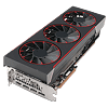
XFX Radeon RX 7900 XTX Magnetic Air Review
(77 Comments) »Introduction
XFX sprung a surprise along the sidelines of the 2024 Computex with their innovative new Radeon RX 7900 XTX Mercury Magnetic Air. This custom-design graphics card powered by AMD's flagship GPU is a step up from the company's top Merc 310 product. It started life out as the China-exclusive RX 7900 XTX Phoenix Nirvana, before the company decided to give the card a worldwide launch as the RX 7900 XTX Magnetic Air. Behind the name is an XFX innovation with the card's fan design. You might see the name "MagAir" or "Mag Air" in some places and stores, but XFX decided to change the name of the product to "Magnetic Air" a few days ago.
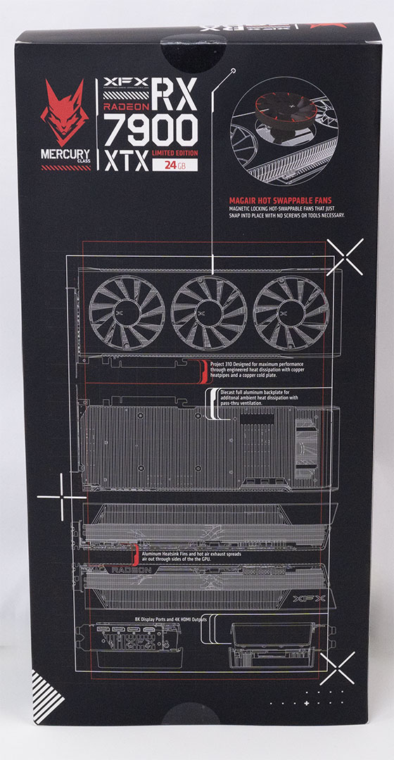
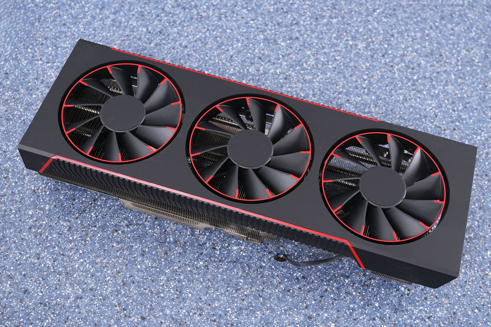
Several graphics card manufacturers are beginning to see the value in making the fans of their cooling solutions easily replaceable by end-users, with minimal need for disassembly. This is to let users clean the fans, for consistent cooling performance. The way they usually go about doing this is by making it straightforward to take off the cooler shroud without disturbing the heatsink underneath. Other companies make it easy to unscrew the fans off their cavities from the cooler shroud, but this needs a screwdriver to access three screws from between the fan blades, making you run the risk of bending or breaking the blades, which could imbalance the fan and damage its bearing down the line. XFX took a novel approach to this problem. The fans can be simply pulled off like fridge magnets, with no tools needed!

Each of the three fans on the XFX RX 7900 XTX Mercury Magnetic Air comes with magnetized grooves behind the hub that interlock with grooves on the cooler shroud, and secured in place by magnetism that's strong enough to hold the fan in place even at its highest RPM. This magnetism, however, is weak enough that a user can pull the fan off without bending or deforming the impeller in the process. There are no wires involved, the grooves have contact points for the four pins of the fan that include power, PWM signal, and speed sensor. There's more to this card than its innovative fan design. The aluminium fin-stack heatsink is improved over the XFX RX 7900 XTX Merc 310. The designs of the cooler shroud and backplate expose a lot more of the heatsink along the top- and bottom edges, improving exhaust ventilation.
AMD Radeon RX 7900 XTX is the company's flagship GPU, designed for maxed out gameplay at 4K Ultra HD, including with ray tracing. It's the most scaled out implementation of the RDNA 3 graphics architecture, which seeks to introduce generational performance and efficiency uplifts riding on the 5 nm foundry node; AI acceleration on the GPU, and a second generation implementation of AMD's ray tracing hardware pipeline that improves ray intersection performance by 50%. The new multi-draw indirect accelerator (MDIA) can significantly improve performance of DirectX 12 applications that use the multi-draw indirect instruction.
The RDNA 3 compute unit design offers a 17% generational performance uplift and support for newer math formats. This uplift, coupled with increased engine clocks, memory bandwidth, and an overall increase in the compute unit count, translates to a 50% shader performance uplift over the previous generation RX 6900 XT. AMD has increased the memory size to 24 GB, and widened the memory bus to 384-bit, besides running the memory at a higher 20 Gbps speed, for a massive 87% increase in memory bandwidth which allowed for a generational reduction of the Infinity Cache size to 96 MB, down from 128 MB.
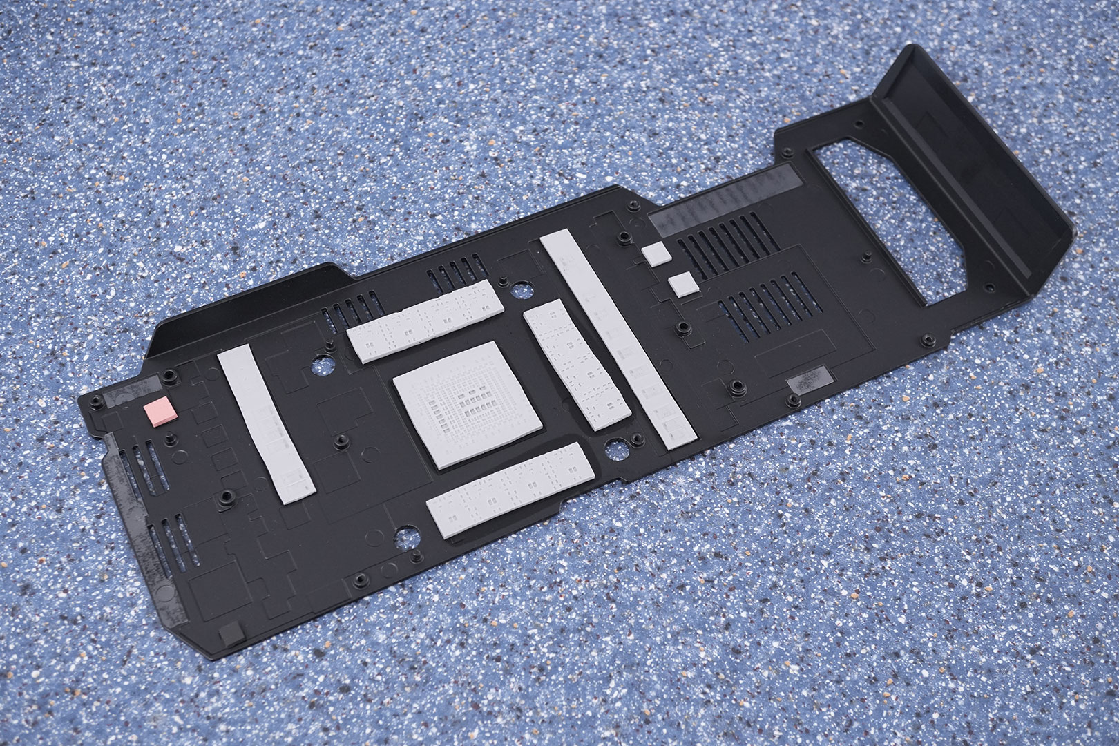
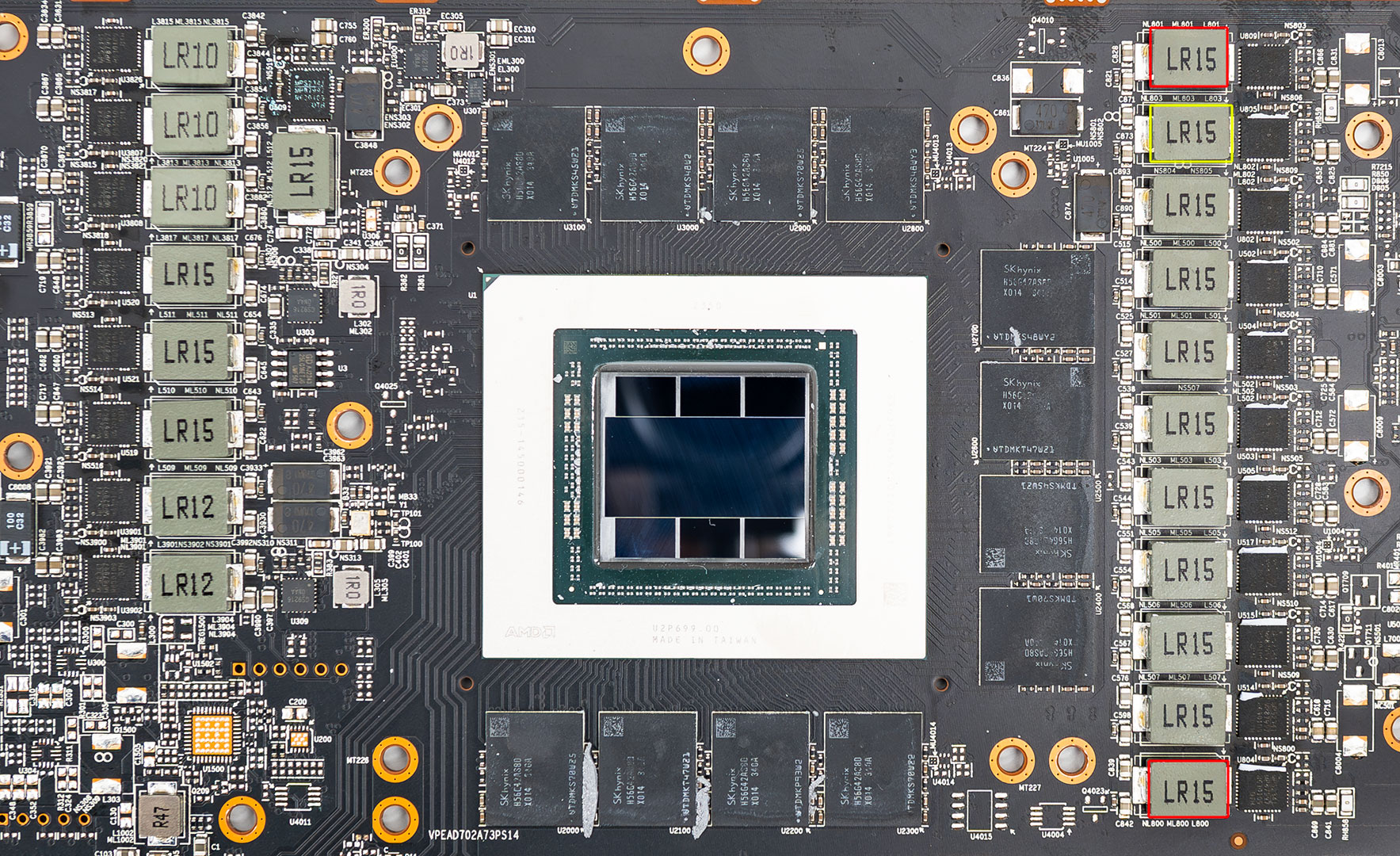
The Radeon RX 7900 XTX is based on "Navi 31," which is the first gaming GPU to use a chiplet architecture. AMD identified all the logic-heavy components that benefit from the switch to 5 nm from 7 nm, and clumped them into a large central chiplet called the graphics compute die (GCD) built on 5 nm, while the other components that don't benefit as much from the switch, namely the Infinity Cache and the memory controllers, are disaggregated into six small chiplets called memory cache dies (MCDs), built on the 6 nm node. Each MCD has a 16 MB segment of the Infinity Cache, and a 64-bit portion of the 384-bit memory bus.
The RX 7900 XTX maxes out the "Navi 31" GPU, enabling all 96 compute units, and all 6 MCDs. You hence have 6,144 stream processors, 96 Ray accelerators, 192 AI accelerators; 384 TMUs, and a staggering 192 ROPs. The GPU's frontend runs at a higher frequency than the shader engines. AMD has given the RX 7900 XTX a Game clock of 2365 MHz, and 2498 MHz boost clock. The memory, as we mentioned, ticks at 20 Gbps, yielding 960 GB/s of memory bandwidth. XFX has overlocked the GPU to 2482 MHz Game clock, and 2615 MHz boost. The card features a dual-BIOS, with the default OC BIOS enabling these clocks and the second BIOS increasing the power limit a bit above stock. Another novelty is that the thermal paste used is Honeywell PTM7950, a phase change material that should provide superior performance and longevity over typical pastes. XFX is pricing the Radeon RX 7900 XTX Mercury Magnetic Air at $980.
| Price | Cores | ROPs | Core Clock | Boost Clock | Memory Clock | GPU | Transistors | Memory | |
|---|---|---|---|---|---|---|---|---|---|
| RTX 4070 | $525 | 5888 | 64 | 1920 MHz | 2475 MHz | 1313 MHz | AD104 | 35800M | 12 GB, GDDR6X, 192-bit |
| RX 7800 XT | $480 | 3840 | 96 | 2124 MHz | 2430 MHz | 2425 MHz | Navi 32 | 28100M | 16 GB, GDDR6, 256-bit |
| RX 6900 XT | $650 | 5120 | 128 | 2015 MHz | 2250 MHz | 2000 MHz | Navi 21 | 26800M | 16 GB, GDDR6, 256-bit |
| RX 6950 XT | $700 | 5120 | 128 | 2100 MHz | 2310 MHz | 2250 MHz | Navi 21 | 26800M | 16 GB, GDDR6, 256-bit |
| RTX 3090 | $800 | 10496 | 112 | 1395 MHz | 1695 MHz | 1219 MHz | GA102 | 28000M | 24 GB, GDDR6X, 384-bit |
| RTX 4070 Super | $585 | 7168 | 80 | 1980 MHz | 2475 MHz | 1313 MHz | AD104 | 35800M | 12 GB, GDDR6X, 192-bit |
| RX 7900 GRE | $530 | 5120 | 160 | 1880 MHz | 2245 MHz | 2250 MHz | Navi 31 | 57700M | 16 GB, GDDR6, 256-bit |
| RTX 4070 Ti | $740 | 7680 | 80 | 2310 MHz | 2610 MHz | 1313 MHz | AD104 | 35800M | 12 GB, GDDR6X, 192-bit |
| RTX 4070 Ti Super | $800 | 8448 | 112 | 2340 MHz | 2610 MHz | 1313 MHz | AD103 | 45900M | 16 GB, GDDR6X, 256-bit |
| RX 7900 XT | $690 | 5376 | 192 | 2000 MHz | 2400 MHz | 2500 MHz | Navi 31 | 57700M | 20 GB, GDDR6, 320-bit |
| RTX 3090 Ti | $1000 | 10752 | 112 | 1560 MHz | 1950 MHz | 1313 MHz | GA102 | 28000M | 24 GB, GDDR6X, 384-bit |
| RTX 4080 | $1000 | 9728 | 112 | 2205 MHz | 2505 MHz | 1400 MHz | AD103 | 45900M | 16 GB, GDDR6X, 256-bit |
| RTX 4080 Super | $970 | 10240 | 112 | 2295 MHz | 2550 MHz | 1438 MHz | AD103 | 45900M | 16 GB, GDDR6X, 256-bit |
| RX 7900 XTX | $910 | 6144 | 192 | 2300 MHz | 2500 MHz | 2500 MHz | Navi 31 | 57700M | 24 GB, GDDR6, 384-bit |
| XFX RX 7900 XTX Magnetic Air | $980 | 6144 | 192 | 2482 MHz | 2500 MHz | 2615 MHz | Navi 31 | 57700M | 24 GB, GDDR6, 384-bit |
| RTX 4090 | $1740 | 16384 | 176 | 2235 MHz | 2520 MHz | 1313 MHz | AD102 | 76300M | 24 GB, GDDR6X, 384-bit |
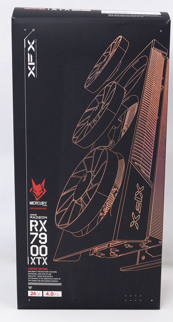
Packaging
The Card
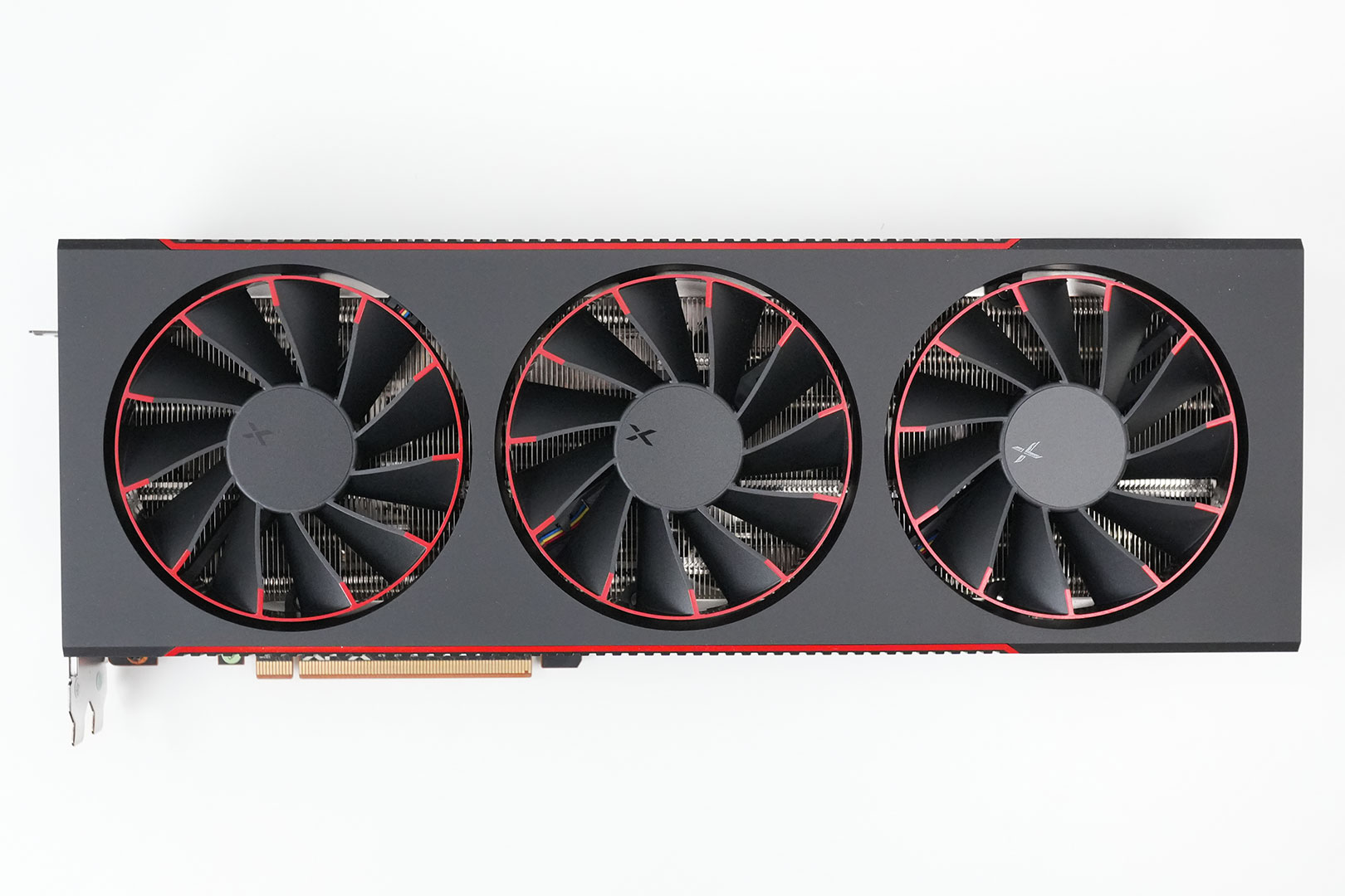
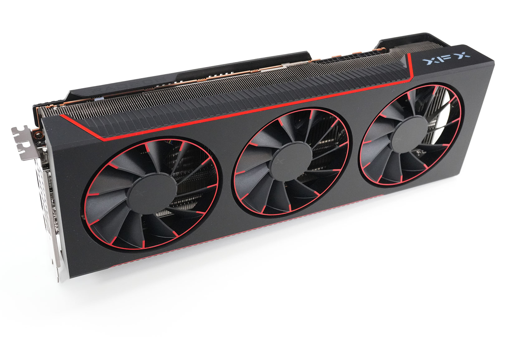
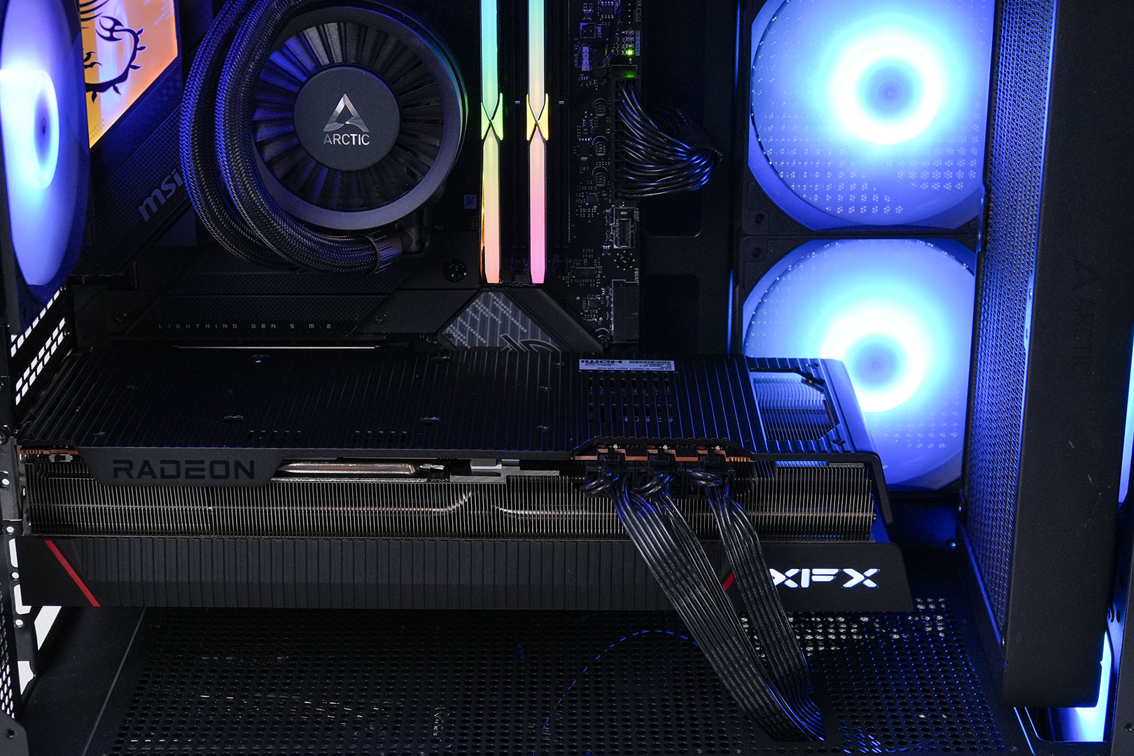
The XFX RX 7900 XTX Magnetic Air introduces a fresh new design that looks mighty good. The design language is very clean, with some red highlights around the fans and along the top edge of the card. On the other side you'll find a metal backplate that has a cutout for air to flow through.
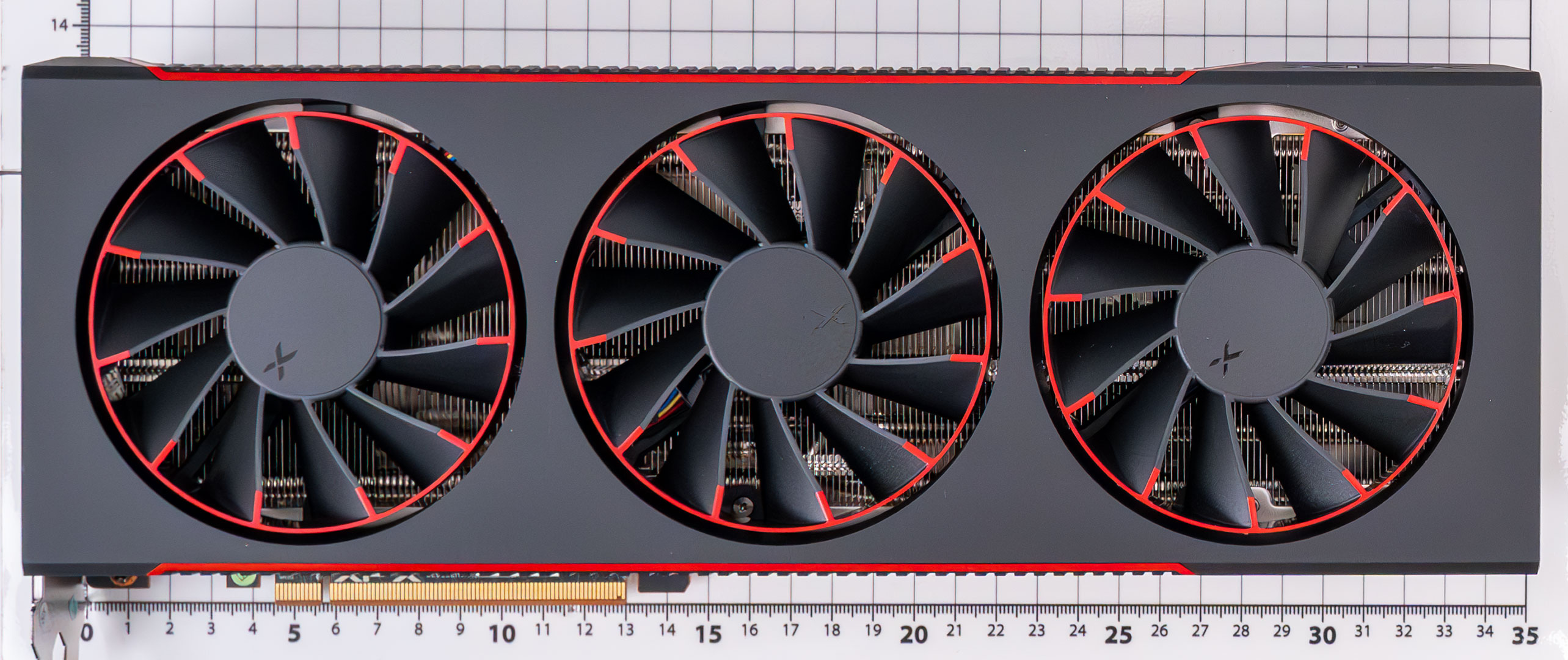

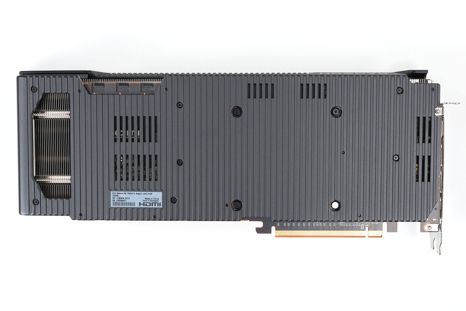
Dimensions of the card are 34.5 x 13.5 cm, and it weighs 1863 g.
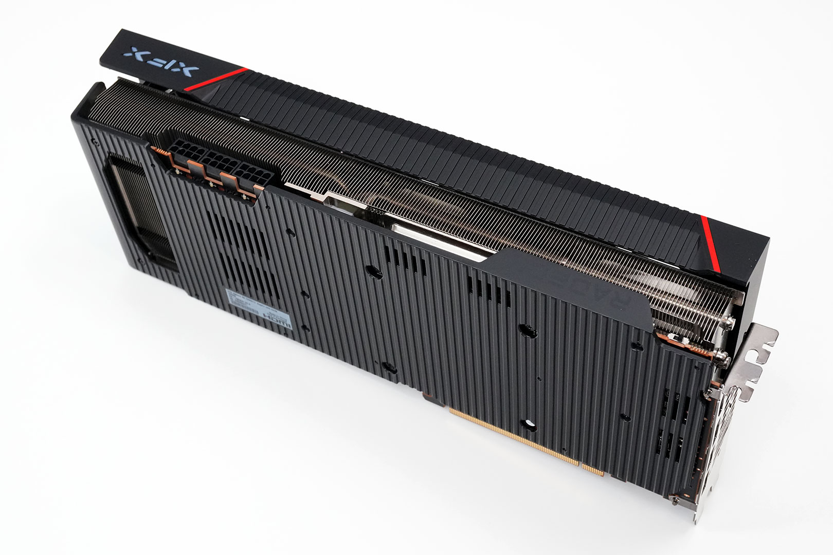
Installation requires three slots in your system. We measured the card's width to be 68 mm.

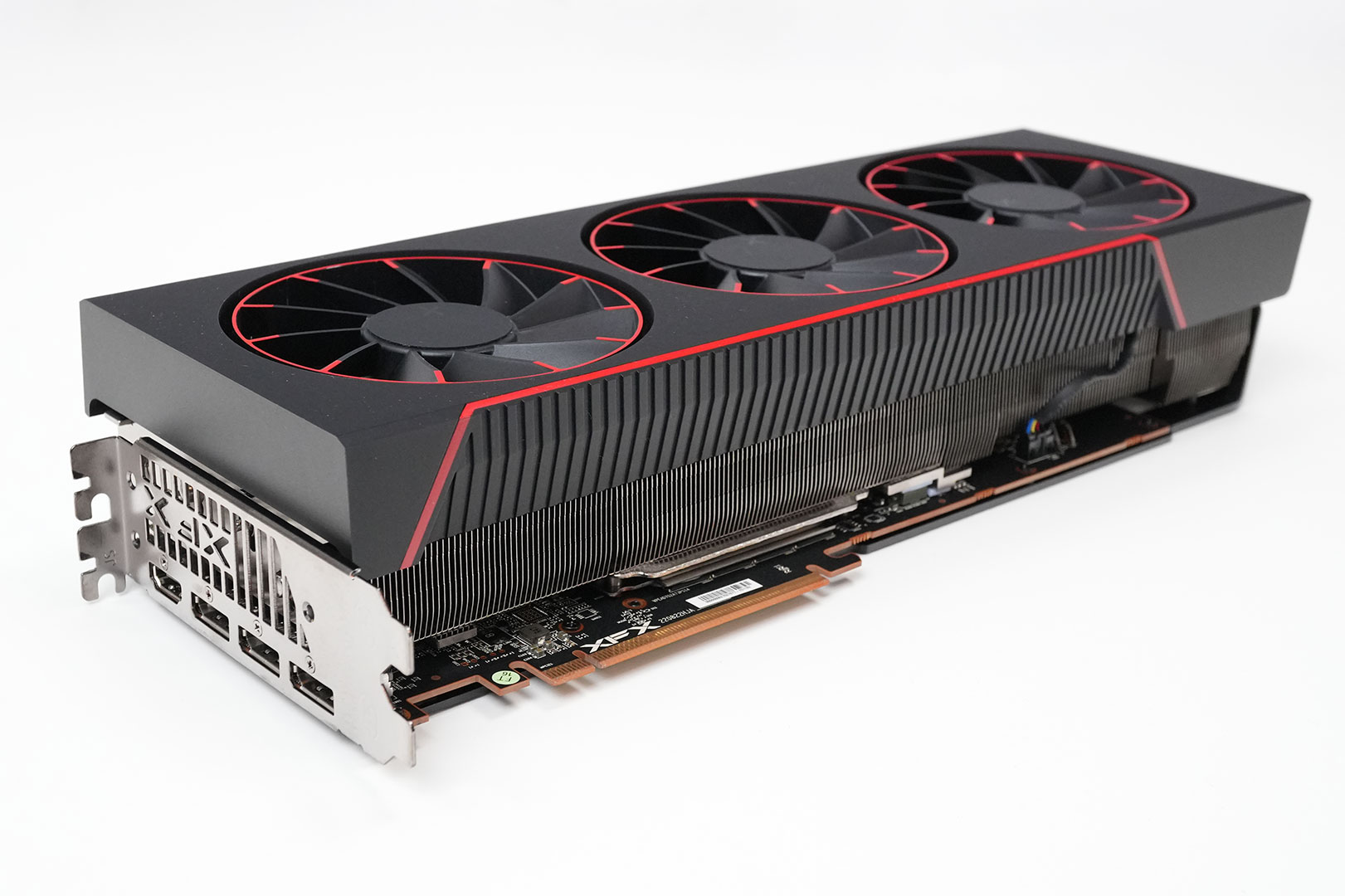
Display connectivity includes three standard DisplayPort 2.1 ports (RDNA 2 had 1.4a) and one HDMI 2.1a (same as RDNA 2).
AMD has upgraded their encode/decode setup. It now comes with two independent hardware units that can encode and decode two streams of video in parallel, or one stream at double the FPS rate. There's support for VP9, H.264, H.265 and AV1 decode, and encoding is supported for H.264, H.265 and AV1.

The card uses a classic triple 8-pin plus PCIe slot power input config, rated for 575 W maximum power.
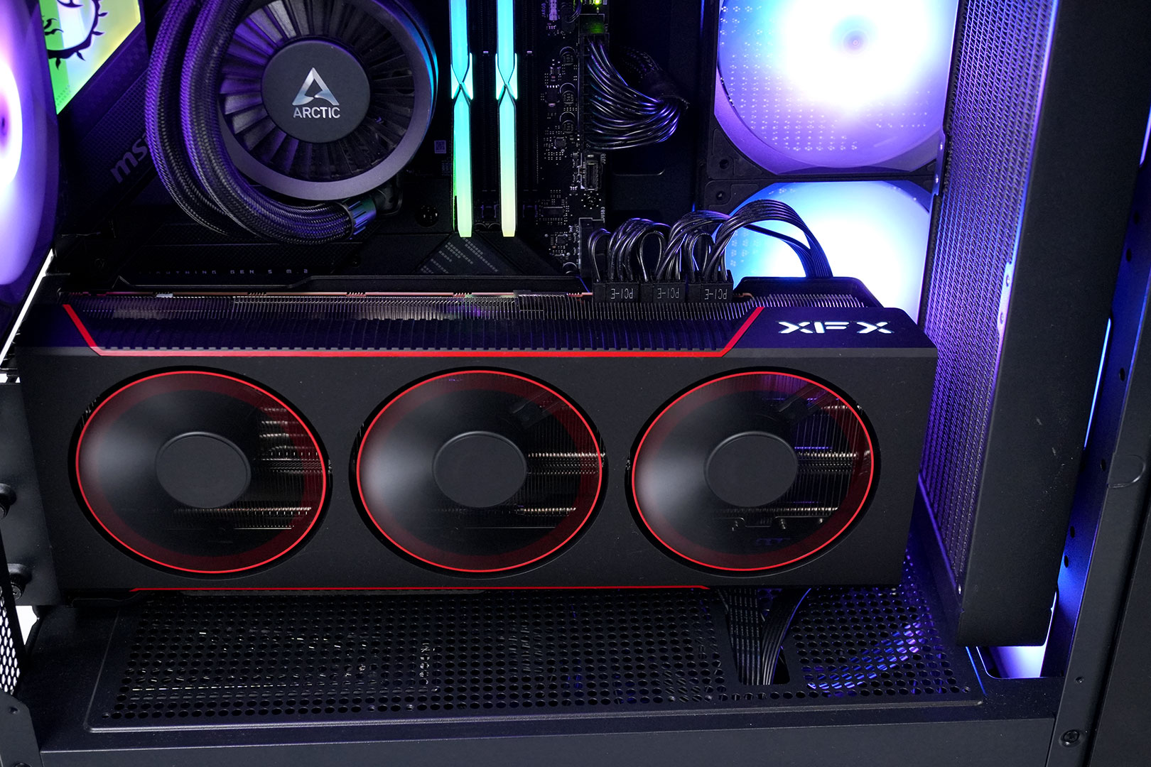
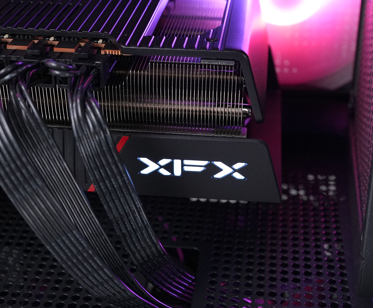
The card comes with a white-illuminated XFX logo, the color is fixed and can't be changed (or turned off).
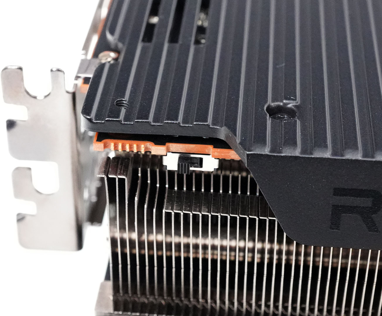
The dual BIOS switch lets you switch to a secondary "higher power target" BIOS.
Teardown
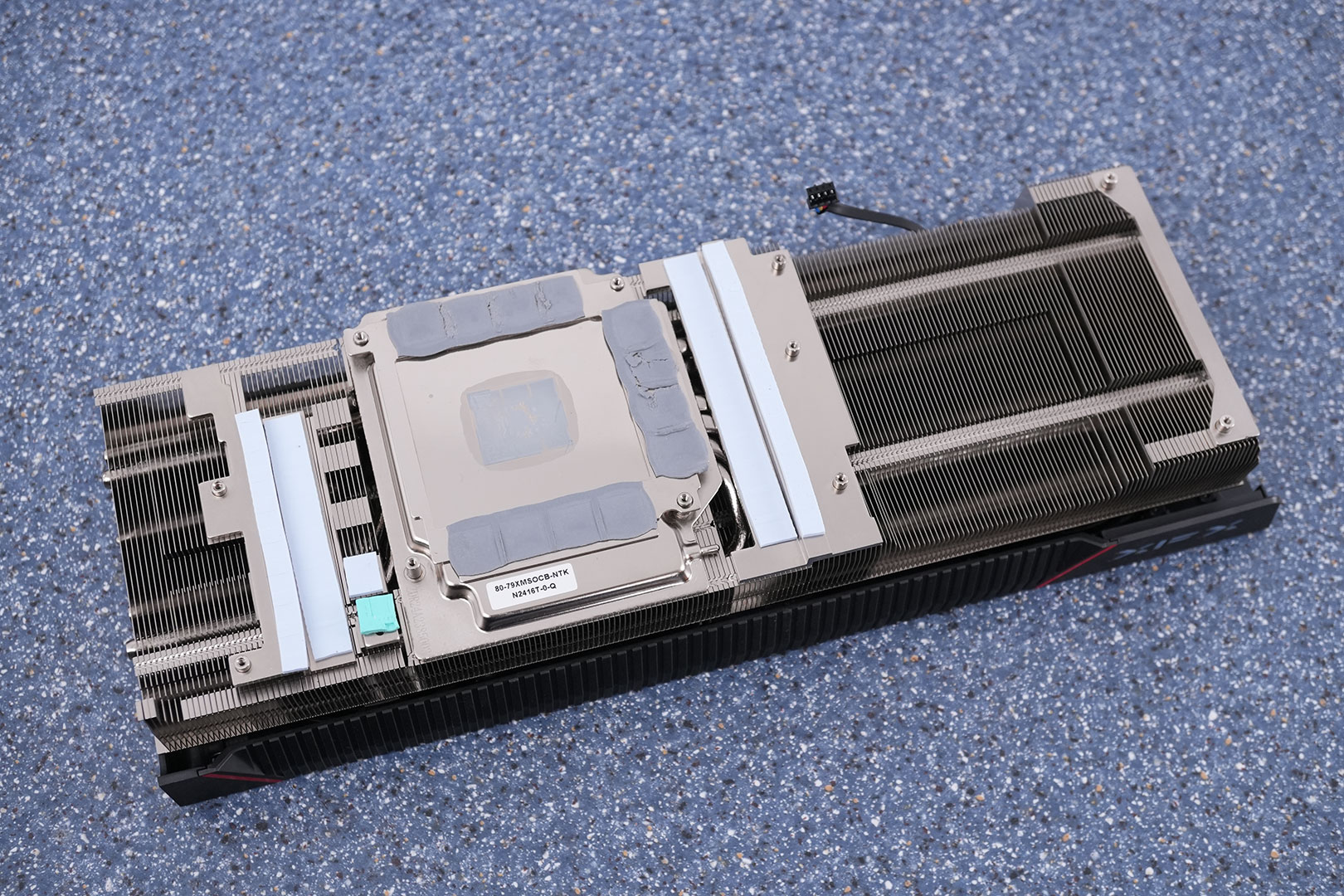
The thermal solution on the XFX RX 7900 XTX Magnetic Air uses a vapor-chamber and has eight heatpipes. The main heatsink also provides cooling for the memory chips and VRM circuitry.


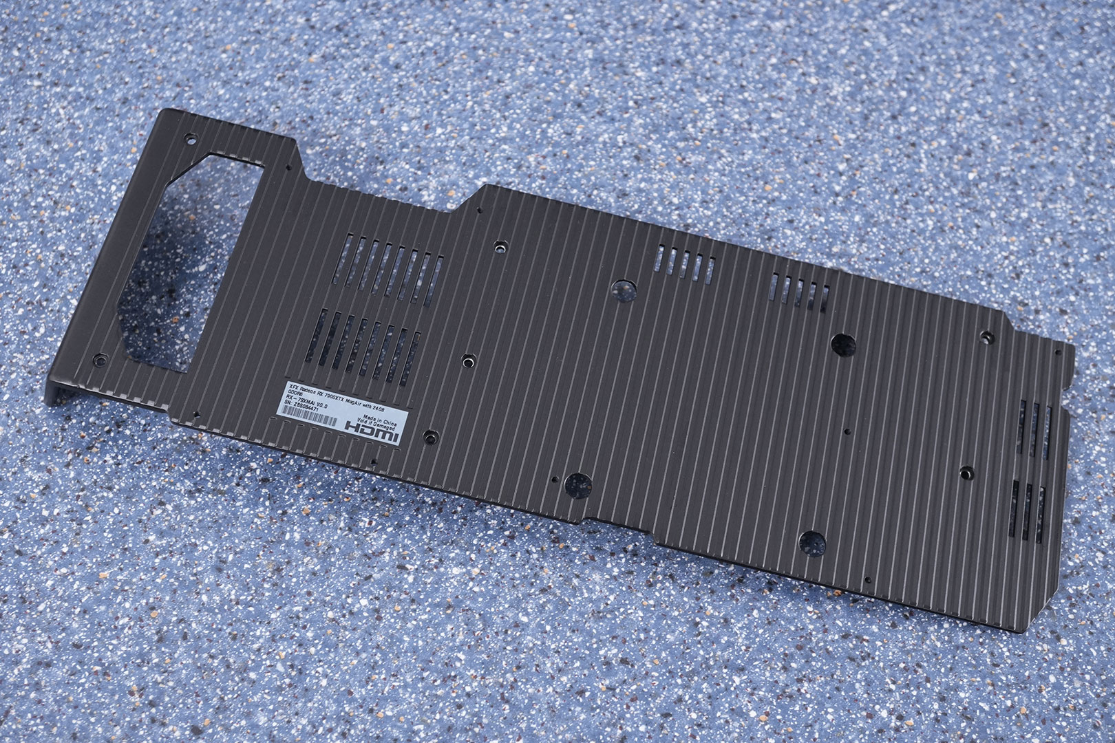
The backplate is made of thick metal and protects the card against damage during installation and handling, as well as reduces GPU sag once installed. It is also curved, which improves the look and feel of the product.
Magnetic Air Fans
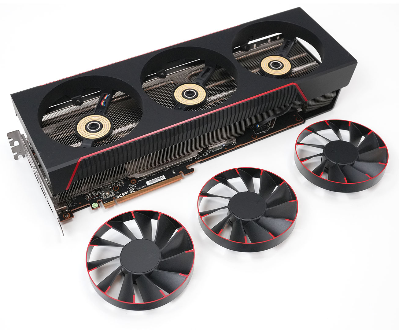
This is the highlight of the new "Magnetic Air" lineup by XFX. The fans can be removed easily, without any tools in just a second or two. Gently pull them upwards and they will come off.
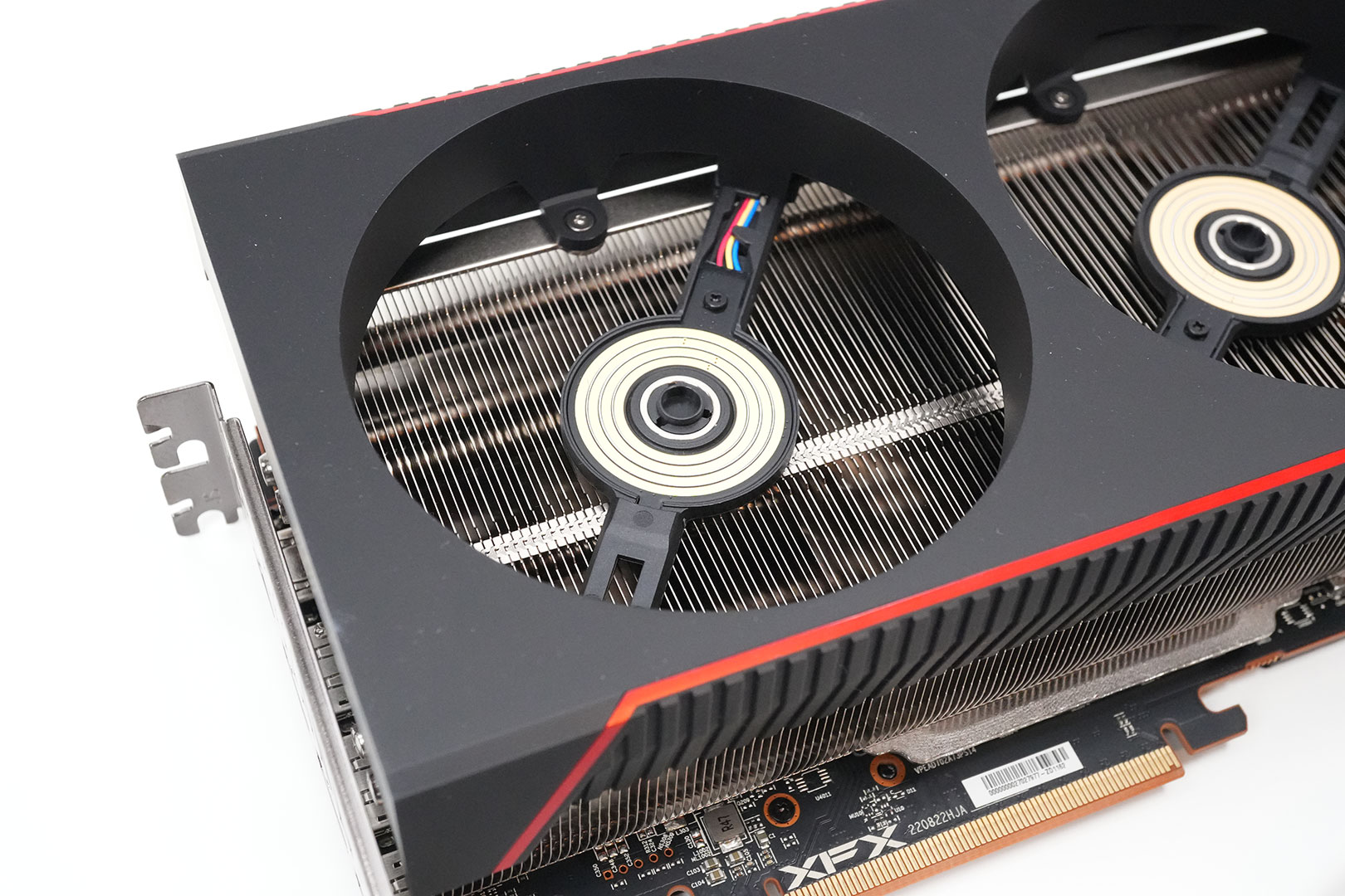
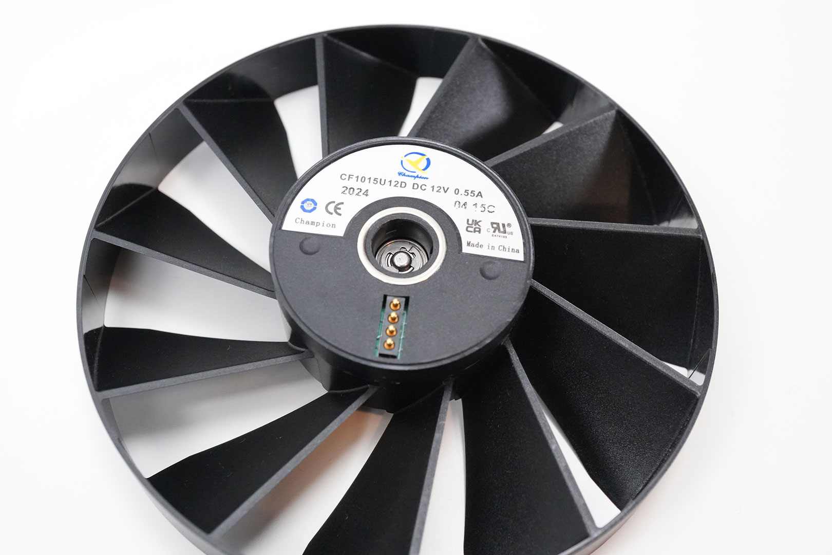
Note the inner "circles" of electrical contact area, which ensure that the four contact pins (second picture) make contact no matter how you place the fan. This inner part (with the contacts and sticker) does not move when the fans are turning, so there's no risk of scraping off the contact area.
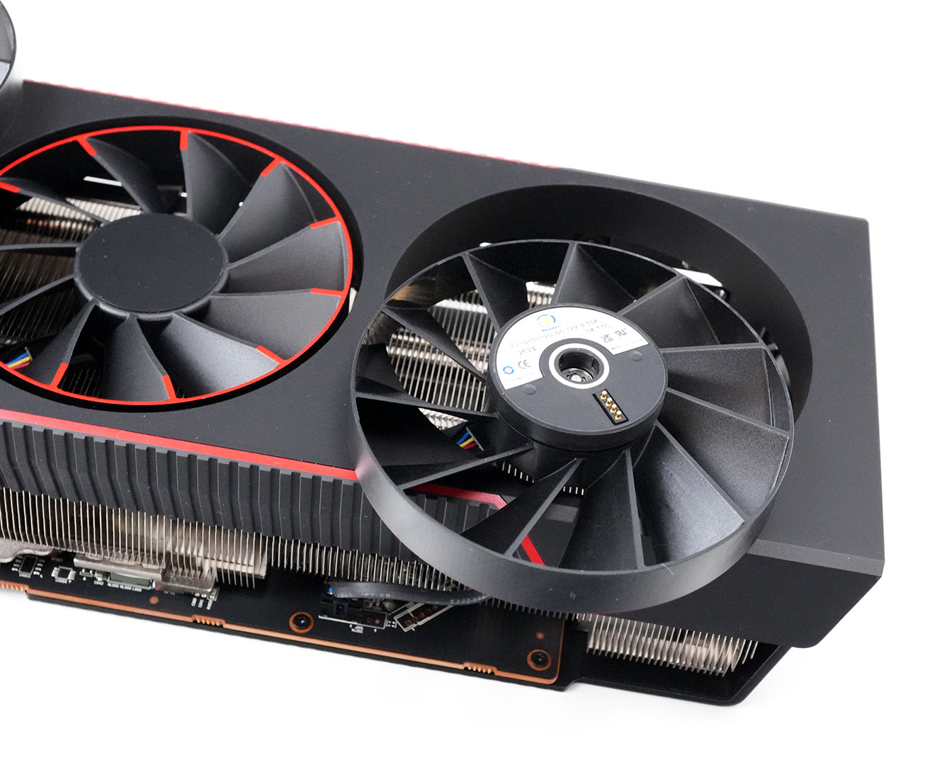

The fans are precision-engineered, everything is of excellent build quality.
High-resolution PCB Pictures
These pictures are for the convenience of volt modders and people who would like to see all the finer details on the PCB. Feel free to link back to us and use these in your articles, videos or forum posts.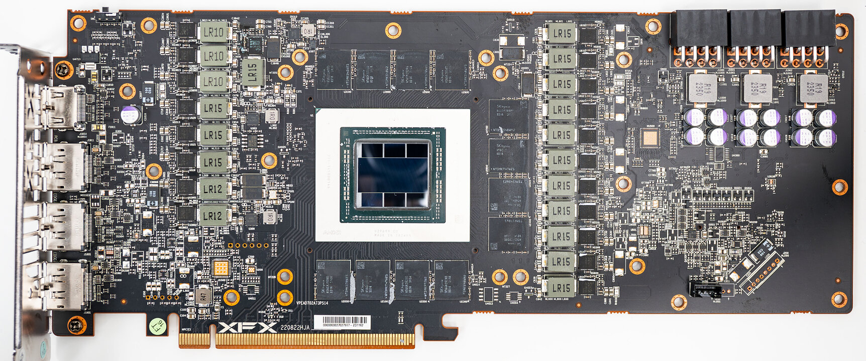

High-resolution versions are also available (front, back).
Circuit Board (PCB) Analysis


GPU voltage is a 17-phase design, managed by a Monolithic Power Systems MP2857 controller.
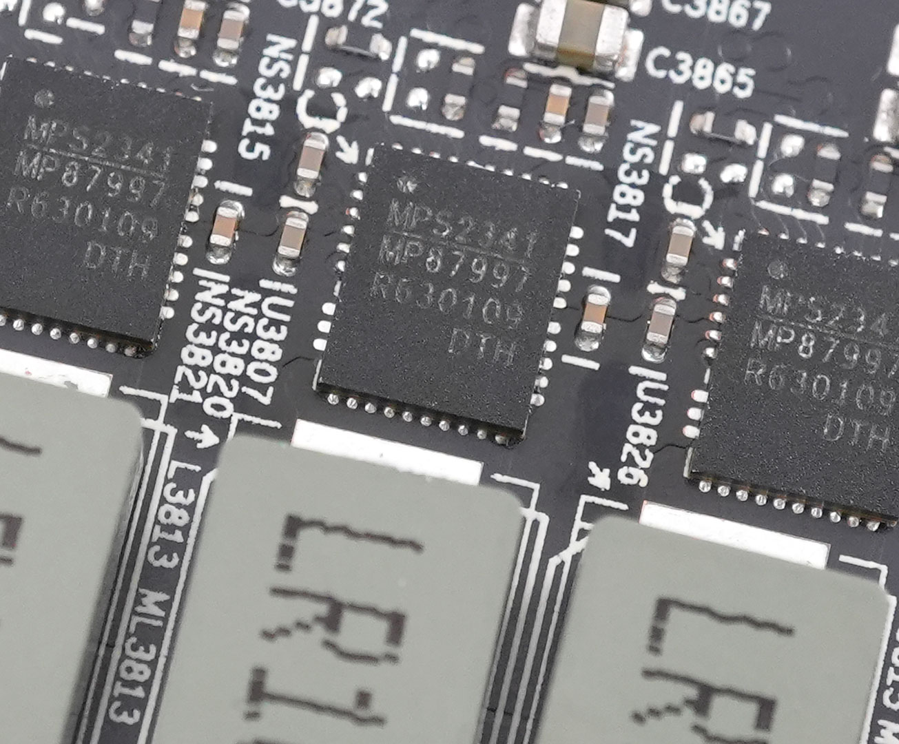
Monolithic MP87997 DrMOS components are used for GPU voltage; they are rated for 70 A of current each.
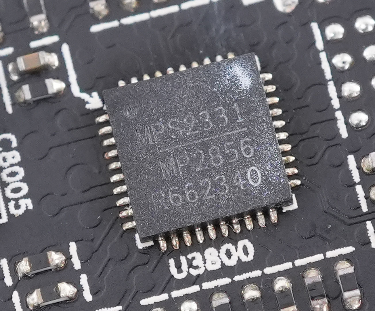
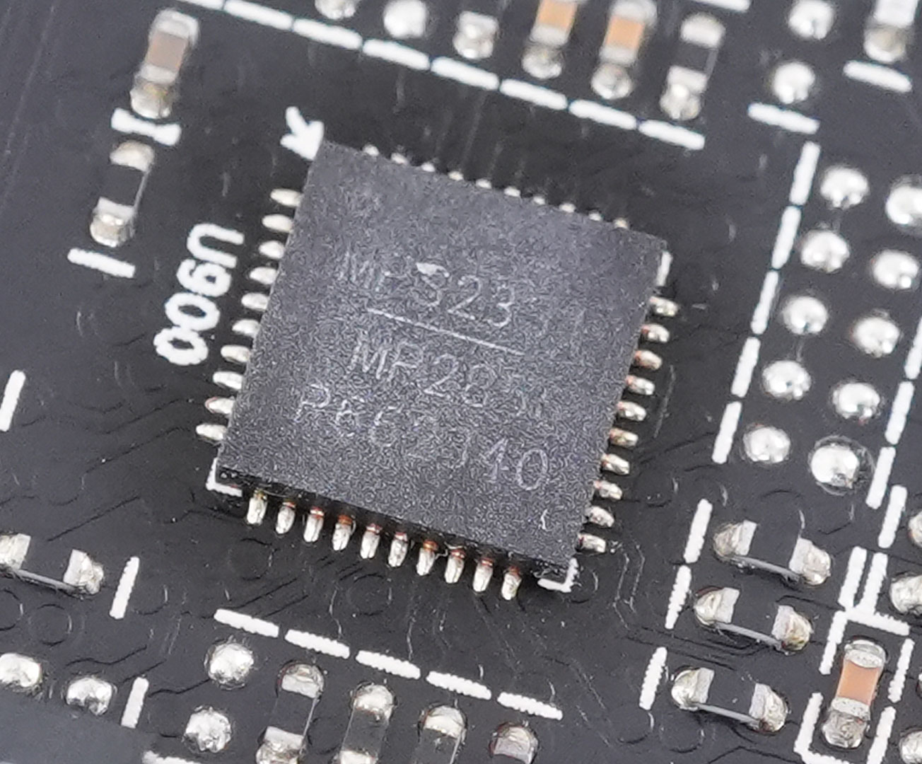
Memory voltage is a 2+1-phase design, managed by two Monolithic Power Systems MP2856 controllers.
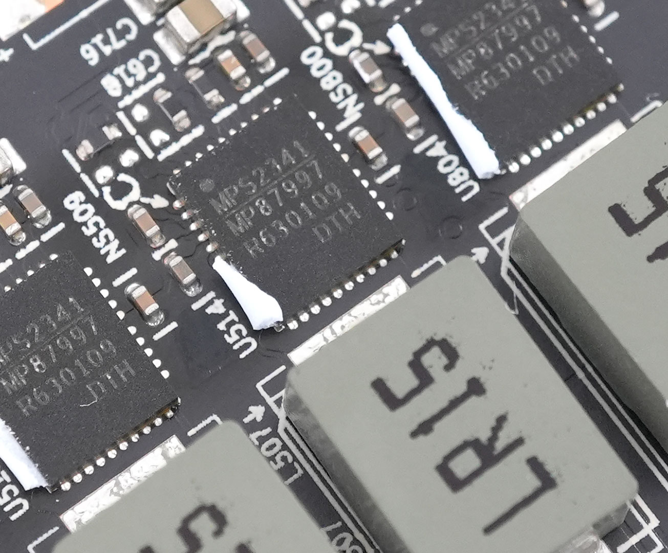
For memory, Monolithic MP87997 DrMOS with a 70 A rating are used here, too.
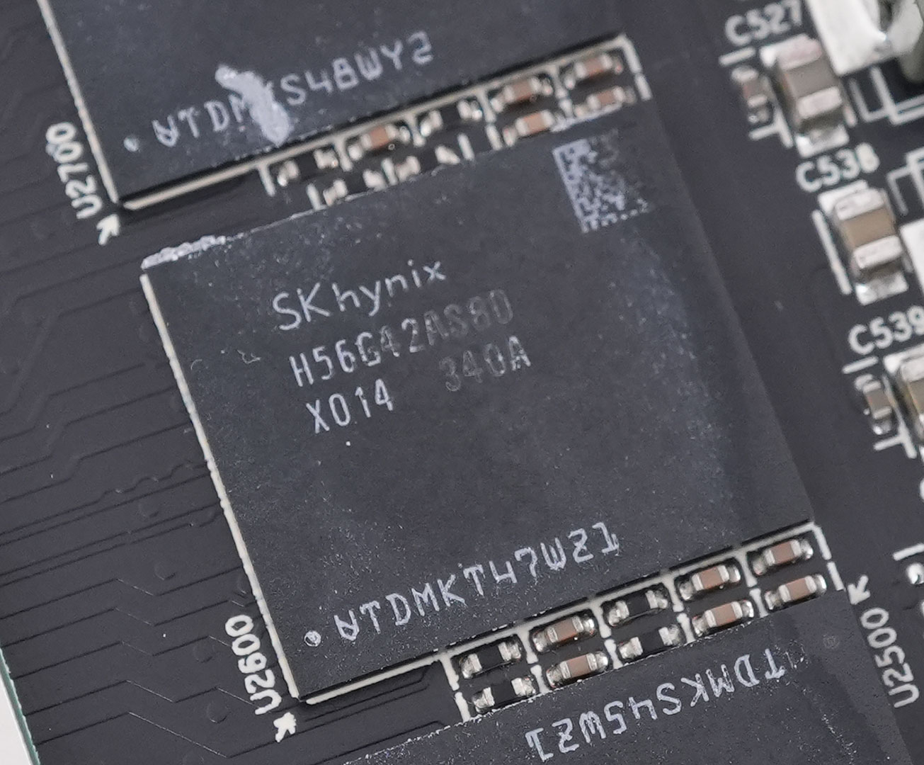
The GDDR6 memory chips are made by Hynix and carry the model number H56G42AS8DX-014. They are specified to run at 2500 MHz (20 Gbps effective).
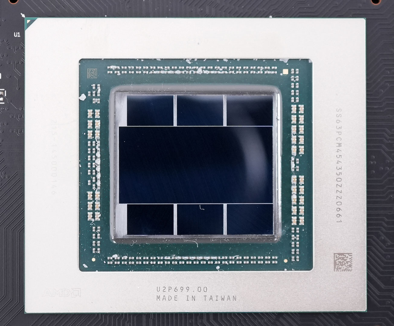
AMD's Navi 31 graphics processor was the world's first GPU that uses a chiplet architecture. Note the large die in the center, called "GCD," graphics compute die, which houses the compute units, it is surrounded by six smaller "MCD," memory cache dies, that contain one memory controller interface and one slice of cache each. While they look similar, the MCDs are not HBM chips. The MCDs are fabricated on a 6 nm process at TSMC Taiwan with a die size of 36.6 mm² each, the GCD is fabricated using TSMC's 5 nanometer node, with a die size of 300 mm². The combined transistor count of the GPU is 57.7 billion.
Our Patreon Silver Supporters can read articles in single-page format.
Mar 12th, 2025 17:03 EDT
change timezone
Latest GPU Drivers
New Forum Posts
- Post your Old CDs & FDs, from back in the day thread. (62)
- Post your Cinebench R23 Score (3053)
- Post your Cinebench 2024 score (619)
- 2006 Macbook Pro Modern Sleeper Project (5)
- 3D Printer Club (449)
- I'm looking for a good tool to make the 3D scanning of my mini-pc using the photogrammetry and my Kinect 2. (66)
- wierd case of 2 equal laptops (1)
- TPU's Nostalgic Hardware Club (20089)
- Intel Optane SSD 905P Series (960GB) for $349.99 (3)
- Share your AIDA 64 cache and memory benchmark here (3032)
Popular Reviews
- AMD Ryzen 9 9950X3D Review - Great for Gaming and Productivity
- XFX Radeon RX 9070 XT Mercury OC Magnetic Air Review
- Sapphire Radeon RX 9070 XT Nitro+ Review - Beating NVIDIA
- ASUS Radeon RX 9070 TUF OC Review
- Dough Spectrum Black 32 Review
- MSI MAG B850 Tomahawk Max Wi-Fi Review
- FSP MP7 Black Review
- AMD Ryzen 7 9800X3D Review - The Best Gaming Processor
- NVIDIA GeForce RTX 5070 Founders Edition Review
- Corsair Vengeance RGB CUDIMM DDR5-8800 48 GB CL42 Review
Controversial News Posts
- NVIDIA GeForce RTX 50 Cards Spotted with Missing ROPs, NVIDIA Confirms the Issue, Multiple Vendors Affected (513)
- AMD Radeon RX 9070 and 9070 XT Listed On Amazon - One Buyer Snags a Unit (261)
- AMD RDNA 4 and Radeon RX 9070 Series Unveiled: $549 & $599 (260)
- AMD Mentions Sub-$700 Pricing for Radeon RX 9070 GPU Series, Looks Like NV Minus $50 Again (249)
- NVIDIA Investigates GeForce RTX 50 Series "Blackwell" Black Screen and BSOD Issues (244)
- AMD Radeon RX 9070 and 9070 XT Official Performance Metrics Leaked, +42% 4K Performance Over Radeon RX 7900 GRE (195)
- AMD Radeon RX 9070-series Pricing Leaks Courtesy of MicroCenter (158)
- AMD Radeon RX 9070 XT Could Get a 32 GB GDDR6 Upgrade (100)