Thursday, October 1st 2009

NVIDIA 'Fermi', Tesla Board Pictured in Greater Detail, Non-Functional Dummy Unveiled
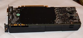
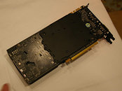
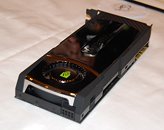
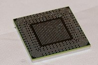
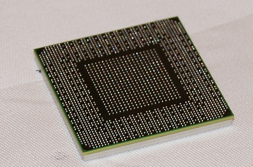
Unveiled at the footnote of the GPU Technology Conference 2009, by none other than NVIDIA CEO Jen-Hsun Huang, NVIDIA's Fermi architecture looks promising, at least in the field of GPGPU, which was extensively discussed upon in his address. The first reference board based on NVIDIA's newest 'GT300' GPU is a Tesla HPC processor card, which quickly became the face of the Fermi architecture. Singapore HardwareZone, and PCPop caught some of the first closeup pictures of the Tesla accelerator, and the GPU's BGA itself. Decked in a dash of chrome, the Tesla HPC processor card isn't particularly long, instead a great deal of compacting by its designers is evident. It draws power from one 8-pin, and 6-pin PCI-E power connectors, which aren't located next to each other. The cooler's blower also draws air from openings in the PCB, and a backplate further cools the GPU (and possibly other components located) from behind. From the looks of it, the GPU package itself isn't larger than that of the GT200 or its predecessor, the G80. Looks like NVIDIA is ready with a working prototype against all odds, after all, doesn't it? Not quite. On close inspection of the PCB, it doesn't look like a working sample. Components that are expected to have pins protruding soldered on the other side, don't have them, and the PCB seems to be abruptly ending. Perhaps it's only a dummy made to display at GTC, and give an indication of how the card ends up looking like. In other words, it doesn't look like NVIDIA has a working prototype/sample of the card they intended to have displayed the other day.
Sources:
Singapore HardwareZone, PCPop


94 Comments on NVIDIA 'Fermi', Tesla Board Pictured in Greater Detail, Non-Functional Dummy Unveiled
Given the fan hole, I'd assume it's from a 9800 GX2 or GTX 295 - except neither of those have dual SLI connectors, and this PCB definitely looks like it was fabricated with both of those connectors.
I have to say that I'm disappointed with nVidia. I've never had much respect for the smoke and mirrors BS that marketing people continually pull, and for nV to allow their marketing department to have their way with this "launch" is not a good sign. While I flat-out cannot believe the "2% yields" rumour, I do believe that nVidia are having a lot more trouble with GT300 than they're letting on.
All of which, of course, is good for ATI and the consumer. Until GT300 finally appears - and that will probably be after Christmas - ATI will rule the roost, which will hopefully pull more developers away from TWIMTBP and (of course) help ATI's bottom line.
ATI have done very well in this round of the "video card wars", and I applaud them. If I do buy a graphics card this year, it will be an ATI.
Edit: One thing no-one mentioned, was that they actually said to the photographers that it is just a mock-up...
forum.beyond3d.com/showthread.php?p=1343173#post1343173
Edit: From AnandTech:
Stockholders probably like how Nvidia is optimistic enough to show a non-functional prototype, just to show what the overall card looks like, but to be caught red-handed in trying to fool us like as if we are such idiots and then confessing it later as a fake card...
Personally, I think it hurts Nvidia overall to do this kind of thing. At least they should have never allowed any close-up pictures to be taken of this fake card.
I do not think Nvidia is really that dumb to shoot itself in the foot for nothing. Perhaps Nvidia is doing this to try to get ATI to be overly complacent for the following months (slacking off with their pending 5870X2 and 5890 launches) and then shock everybody with a hard launch of GT300 cards as early as December.
Look on the back of the card; what a lame ass thing to do.
And you can't say they have done very good in this round yet, when the round has just begun. You wouldn't say a boxer won the match before the second boxer even stepping in the ring, would you?
And my guess would be that the PCB is from an early prototype of the card, and it was modified to give an idea of the look of the final product. This way they aren't showing something that looks nothing like the final product.
In my opinion, the card was a complete fakery. Nothing more than to put "Nvidia shows next gen whatever" in the headines of the buisness page for their shareholders.
As Binge posted in the other thread. The real Fermi: forums.techpowerup.com/showpost.php?p=1579097&postcount=207
Of course, when the card is actually released (and it will be) the point will be moot.
btw. gtx 295 is a dual card, combined with all the problems, dual brings, will it be heat,noise, no space etc:p
(just thought I'd finish that off with a more... direct statement of how you feel;))
Even now the specifications for the R900 are closed but the card is not in production yet, with the R1000 GPU itself being currently in development.
The PCB in the picture is probably from a refused prototype of a PCB, could be from any of the 8 series and up, nobody will eva know.