Monday, December 13th 2010

AMD Cayman Taken Apart, PCB Pictured

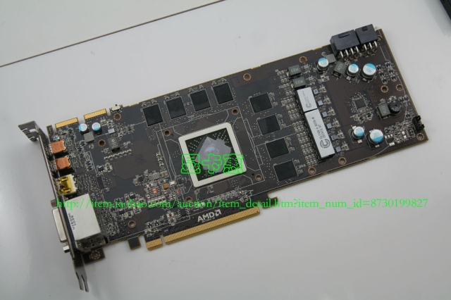
We've seen quite a few pictures of the AMD Radeon HD 6970 from its exterior, including some finer details observable. For the first time, we're getting to take a peek inside, thanks to a Chinese website that looks to be auctioning off an HD 6970 ahead of launch for a quick buck, if we're not terribly mistaken. The PCB shot reveals many details about the GPU and its board design:
  • To begin with, the GPU indeed has a 256-bit wide memory interface, counting the memory chips on the obverse side, and looking at the size of the GPU package.
  • The size of the die, and taken that Cayman is a 40 nm GPU, indicate that Cayman is not much bigger than Cypress, it should be about 400~500 million transistors higher compared to Cypress.
  • Given the roughly 2500 million transistor count, the stream core count of 1536 seems more realistic. AMD is said to be using an architecturally superior VLIW4 stream processor design that increases performance per mm² die area.
  • The board uses a high-grade 6+2+1+1 phase digital PWM voltage regulation design, draws power from 8+6 pin power connectors.
  • The reverse side of the PCB has no memory chips, so AMD might be using 2 Gbit memory chips to get 2 GB of total memory

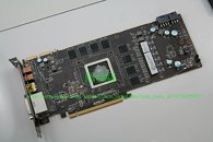
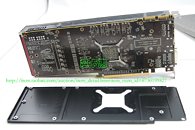
Images Courtesy: Taobao.com
Add your own comment

37 Comments on AMD Cayman Taken Apart, PCB Pictured

#1
gvblake22
Surprisingly clean; almost looks incomplete! Hopefully that means it is efficient. :toast:
Posted on Reply
#2
Delta6326
Yummy!!! can't wait for reviews!!!!!
Posted on Reply
#3
OneCool
Can anyone point out in those pictures where the Texas Instrument chip is that was the "cause" of the delay?I know their small ....but..
Posted on Reply
#4
largon
btarunr
  • (...)
  • The board uses a high-grade 6+2+1+1 phase digital PWM voltage regulation design, draws power from 8+6 pin power connectors.
    (...)
  • 6+2+1+1?
    I see only 6+1+1+1:
    6× Volterra VT1165SF for vGPU
    1× Volterra VT1175SF for vDDCI (GDDR5 memctrl) (near CF fingers)
    1× Volterra VT242WF for memory vDD
    1× Volterra VT242WF for memory vDDQ
Posted on Reply
#5
chuchnit
Looks almost copy/paste of 5870 PCB. Where are all these TI parts that caused the delays?
Posted on Reply
#6
arnoo1
what gtx 400 series and gtx500 series power hungry, amd does the same now lol
fail for amd fanboys


nice card btw
Posted on Reply
#7
Swamp Monster
chuchnitWhere are all these TI parts that caused the delays?
I don't see any TI DrMos here. This card could be test version with different power components. Will see when W1zzard shows review.
Posted on Reply
#8
DanishDevil
Anybody else find it interesting that they switched from having the power circuitry near the display outputs (6870) back to where it is traditionally?
Posted on Reply
#9
KainXS
I just got to see one, seems to trade blows with the 570 but had alot of driver problems mainly inconsistency
Posted on Reply
#10
_JP_
arnoo1what gtx 400 series and gtx500 series power hungry, amd does the same now lol
fail for amd fanboys
Wait, what?!
You either back that up with real info or I'm nailing you to the wall!
Posted on Reply
#11
theonedub
habe fidem
_JP_Wait, what?!
You either back that up with real info or I'm nailing you to the wall!
Prob referring to the 8+6pin connectors on the board, which is a departure from the 5870 which only did dual 6pins. Might be evidence of higher power consumption.
Posted on Reply
#12
AsRock
TPU addict
DanishDevilAnybody else find it interesting that they switched from having the power circuitry near the display outputs (6870) back to where it is traditionally?
Yeah 1st thing i noticed kinda liked the idea but maybe it was to much to put though the whole board so they put them were they normally are. Or maybe cost reason which sounds more like it.

Kinda glad they put it back as now hopefully Thermaltake will do a 3rd party VRM cooler for it :). And hopefully some one will do a screw on type ram cooling unless the older 4970\90 one fits.
Posted on Reply
#13
wolf
Performance Enthusiast
loving the backplate.

backplates float my boat.
Posted on Reply
#14
_JP_
theonedubProb referring to the 8+6pin connectors on the board, which is a departure from the 5870 which only did dual 6pins. Might be evidence of higher power consumption.
It might be that, but it was't said/mentioned. The HD 5870 only had dual 6-pin plugs but there was solder points for a 8+6-pin plug configuration. I guess ATi managed to avoid that in the reference card at that time. Also, considering that the 2 extra pins are grounds, I don't see that as a mandatory increase in power consumption.
Posted on Reply
#15
theonedub
habe fidem
_JP_It might be that, but it was't said/mentioned. The HD 5870 only had dual 6-pin plugs but there was solder points for a 8+6-pin plug configuration. I guess ATi managed to avoid that in the reference card at that time. Also, considering that the 2 extra pins are grounds, I don't see that as a mandatory increase in power consumption.
Its all speculation at this point, I was merely pointing out a possible explanation for that user's comments. The news post does say 8+6 and the PowerColor 6970 also shows 8+6. It is very true that the connectors do not guarantee higher power consumption, but very rarely are they just for show. We shall see :D
Posted on Reply
#16
mtosev
W1zzard's review coming soon:)
Posted on Reply
#17
v12dock
Block Caption of Rainey Street
1536 shaders.... :shadedshu
Posted on Reply
#18
jasper1605
v12dock1536 shaders.... :shadedshu
I swear on my life I'll pistol whip the next person to do a shadedshu in reference to the shader count on a graphics card.
Posted on Reply
#19
CDdude55
Crazy 4 TPU!!!
Still waiting for the reviews.:)
Posted on Reply
#20
Flibolito
The backplates are sexy. As far as power consumption is concerned it's probably going eat more than the 6800s and maybe less that the 500 series but honestly in the high end gpu sector its something that should be expected. High res graphics with all the bells and whistles is going to eat power. I would rather it eat power and compete to bring the prices down, that will save you more money than saving $30 a year on the electric bill. Once my fermi was up and running I saw zero change in my power bill and I'm sure under load its well over 300 watts.
Posted on Reply
#21
v12dock
Block Caption of Rainey Street
jasper1605I swear on my life I'll pistol whip the next person to do a shadedshu in reference to the shader count on a graphics card.
I lost all faith in this card
Posted on Reply
#22
D4S4
sorry guys, but do you hear yourself? just stfu and wait for the damned review. it'll be here soon enough.
Posted on Reply
#23
arnoo1
_JP_Wait, what?!
You either back that up with real info or I'm nailing you to the wall!
no thanks lol

6pin peg connector +8pin peg connector says enough, that around 300wat with the 75 watts you wil get out of the pci-e 2.0 slot
Posted on Reply
#24
[H]@RD5TUFF
jasper1605I swear on my life I'll pistol whip the next person to do a shadedshu in reference to the shader count on a graphics card.
Shaders . . .:shadedshu:roll:
Posted on Reply
#25
Jstn7477
arnoo1no thanks lol

6pin peg connector +8pin peg connector says enough, that around 300wat with the 75 watts you wil get out of the pci-e 2.0 slot
My Sapphire HD 3850 AGP has an 8 pin power connector, but it still runs fine on a 6 pin connector. I'm pretty sure my single slot 3850 AGP does not consume 205w of power, just because it has an 8 pin connector.

Another example: ATI Radeon 5670. Some models come with a 6 pin PCIe connector, others don't. It is highly unlikely that a 400sp chip consumes 150w of power.

TL;DR: Maybe AMD wants us to have some more overclocking headroom. But for now, we should wait for some actual reviews before we go calling this a GTX 480.
Posted on Reply
Add your own comment
May 18th, 2024 22:29 EDT change timezone

New Forum Posts

Popular Reviews

Controversial News Posts