Tuesday, March 13th 2012

GeForce GTX 680 Specifications Sheet Leaked

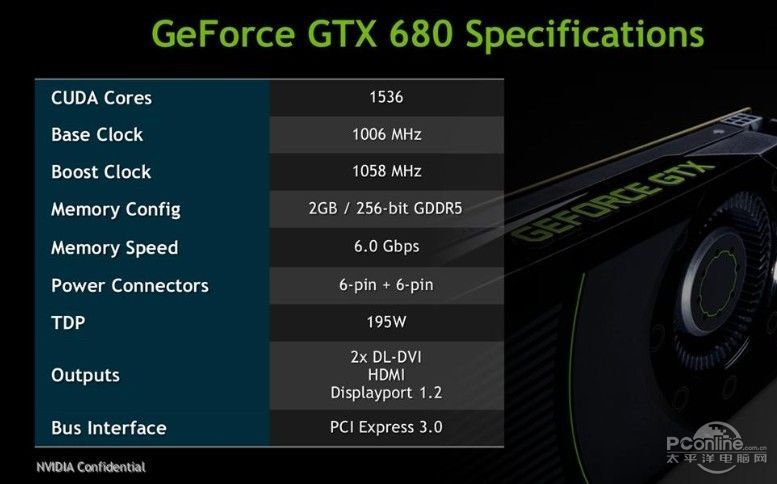
Chinese media site PCOnline.com.cn released what it claims to be an except from the press-deck of NVIDIA's GeForce GTX 680 launch, reportedly scheduled for March 22. The specs sheet is in tune with a lot of information that we already came across on the internet, when preparing our older reports. To begin with the GeForce GTX 680 features clock speeds of 1006 MHz (base), and 1058 MHz (boost). The memory is clocked at a stellar 6.00 GHz (1500 MHz actual), with a memory bus width of 256-bit, it should churn out memory bandwidth of 192 GB/s. 2 GB is the standard memory amount.

For the umpteenth time, this GPU does feature 1,536 CUDA cores. The card draws power from two 6-pin PCIe power connectors. The GPU's TDP is rated at 195W. Display outputs include two DVI, and one each of HDMI and DisplayPort. Like with the new-generation GPUs from AMD, it supports PCI-Express 3.0 x16 bus interface, which could particularly benefit Ivy Bridge and Sandy Bridge-E systems, in cases where the link width is reduced to PCI-Express 3.0 x8 when there are multiple graphics cards installed.
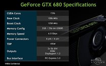
Source: PCOnline.com.cn
Add your own comment

44 Comments on GeForce GTX 680 Specifications Sheet Leaked

#1
Athlon2K15
HyperVtX™
Amazing! Radeon better watch out nvidia is about to release a monster.:)
Posted on Reply
#2
tilldeath
AthlonX2Amazing! Radeon better watch out nvidia is about to release a monster.:)
meh, from what I've seen I'm guessing the power consumption and heat will be way up there. I also doubt OC headroom will be as high as AMD's. So as with everything price will be key and I guess we just have to wait.
Posted on Reply
#3
Stephen.
Other reports said base/core clock of 705 now it's 1006MHz that's not bad at all, but my big question is it GK104 or will it turn out to be GK100 after all,....
Posted on Reply
#4
Sihastru
This will be the "Gigahertz + 6 Edition"?
Posted on Reply
#5
Crap Daddy
This seems to be the real thing.

Was expecting high clocks and no... hotclocks. The boost is somehow... small?
Posted on Reply
#6
btarunr
Editor & Senior Moderator
The way NVIDIA is handling clock-domains on GK104 looks bound to confuse the living shit out of enthusiasts. We'll try to clear this up in our review if neccessary.
Posted on Reply
#7
sanadanosa
It's very very good news that GTX 680 only use a pair of 6 pins
Posted on Reply
#8
Sihastru
If it's just a 5% boost then overclocking the card should not be too much trouble. Hopefully there will be a way to disable boost for those wanting the highest OC possible.
Posted on Reply
#9
ThomasK
1,536 CUDA cores on an 195w thermal envelope? Sounds fake to me.

I'm aware that the new 28nm process brings several benefits to the table, but I really doubt that the new process plus tweaks on NVIDIA's architecture would make viable for them to get roughly three times as much CUDA cores to work at ~1GHz.

Let's just wait for official numbers.
Posted on Reply
#10
Tatty_Two
Gone Fishing
^^^ I have to agree with you there, with that 195W Thermal envelope it's difficult to beleive that they can squeeze 1000mhz+ out of it (although they may easily prove me wrong), maybe thats why the origional info suggested 705mhz..... having said that, to be honest, if the performance is there then probably most will buy it who can afford it and those that are not enthusiasts won't even know it's power draw.
Posted on Reply
#11
Wrigleyvillain
PTFO or GTFO
AthlonX2Amazing! Radeon better watch out nvidia is about to release a monster.:)
lol same comment gen after gen after gen. Not saying it isn't true even just that it's funny how you always hear the exact same shit every time (whether it is true or not).
Posted on Reply
#12
cadaveca
My name is Dave
btarunrThe way NVIDIA is handling clock-domains on GK104 is bound to confuse the living shit out of enthusiasts. We'll dedicate an entire page to making sense of it in our review.
That'd be awesome, as I generally have a good understanding of hardware, but this stuff blows my mind.:laugh:
Wrigleyvillainlol same comment gen after gen after gen. Not saying it isn't true even just that it's funny how you always hear the exact same shit every time (whether it is true or not).
Funny how it needs to be repeated. Personally, because i don't get what's going on with these card, I reserve all judgement until after I get to read W1zz's review, which i guess is incoming at some point.


I'm still laughing at the fact that the "chocolate" was in fact a cookie. That mis-conception alone, based on appearances, says quite a bit.
Posted on Reply
#13
MxPhenom 216
ASIC Engineer
.Tk1,536 CUDA cores on an 195w thermal envelope? Sounds fake to me.

I'm aware that the new 28nm process brings several benefits to the table, but I really doubt that the new process plus tweaks on NVIDIA's architecture would make viable for them to get roughly three times as much CUDA cores to work at ~1GHz.

Let's just wait for official numbers.
well since the Cuda cores have been simplified and less complex and smaller it makes sense. I love when people claim things are fake, but then get proven wrong when the thing releases. I never judge anything till i see Wizz's review, I only remain optimistic.
Posted on Reply
#14
Imsochobo
nvidiaintelftwwell since the Cuda cores have been simplified and less complex and smaller it makes sense. I love when people claim things are fake, but then get proven wrong when the thing releases. I never judge anything till i see Wizz's review, I only remain optimistic.
so amd is making theirs more advanced and nvidia simplify...

anyways, 1536 with 1000 mhz on 195W tdp is abit hard on my brain, not saying it's impossible.
either they are giving up tesla or making a diffrent gpu tree for that if it's true is my guess then.
Posted on Reply
#15
ThomasK
nvidiaintelftwwell since the Cuda cores have been simplified and less complex and smaller it makes sense. I love when people claim things are fake, but then get proven wrong when the thing releases. I never judge anything till i see Wizz's review, I only remain optimistic.
Well, I have the right to claim it's fake since the source is unofficial and 'cause the numbers seem a lil' bit absurd.
Nevertheless, I'd be really impressed if NVIDIA would actually get along with the numbers shown on that spec. sheet, but what I really can't understand (considering that leaked slide to be authentic) is why would NVIDIA favour a lower TDP when they could just crank up some more CUDA cores or even clocks to extend their possible performance leadership?
Posted on Reply
#16
Crap Daddy
.TkWell, I have the right to claim it's fake since the source is unofficial and 'cause the numbers seem a lil' bit absurd.
Nevertheless, I'd be really impressed if NVIDIA would actually get along with the numbers shown on that spec. sheet, but what I really can't understand (considering that leaked slide to be authentic) is why would NVIDIA favour a lower TDP when they could just crank up some more CUDA cores or even clocks to extend their possible performance leadership?
Maybe it's already cranked up?
Posted on Reply
#17
brandonwh64
Addicted to Bacon and StarCrunches!!!
Crap DaddyMaybe it's already cranked up?
Its all hyped up on mountain dew?
Posted on Reply
#18
Crap Daddy
brandonwh64Its all hyped up on mountain dew?
plus a few red bulls
Posted on Reply
#19
Vulpesveritas
Crap Daddyplus a few red bulls
Toss in a few bottles of five hour energy perhaps as well.
Posted on Reply
#20
Benetanegia
Imsochoboso amd is making theirs more advanced and nvidia simplify...

anyways, 1536 with 1000 mhz on 195W tdp is abit hard on my brain, not saying it's impossible.
either they are giving up tesla or making a diffrent gpu tree for that if it's true is my guess then.
Well I don't know if fake or not, but they are not so hard to believe if you think about what is really going on. I bet you are thinking 1536 @ ~1000 Mhz vs 512 @ ~800 Mhz, but that is not the case. It's 1536 @ ~1000 Mhz (not all the time, dynamic clocks) vs 512 @ ~1600 Mhz. Needing to clock only to 1000+ Mhz instead of 1600++ Mhz posibly allows for much smaller, simpler and cooler SPs.

I always use the same example and I know it's not about SPs, but it's one of the most clear ones I can find in recent history, and everything applies to electronics to some extent:

www.anandtech.com/show/3987/amds-radeon-6870-6850-renewing-competition-in-the-midrange-market/2
AMD made one other major change to improve efficiency for Barts: they’re using Redwood’s memory controller. In the past we’ve talked about the inherent complexities of driving GDDR5 at high speeds, but until now we’ve never known just how complex it is. It turns out that Cypress’s memory controller is nearly twice as big as Redwood’s! By reducing their desired memory speeds from 4.8GHz to 4.2GHz, AMD was able to reduce the size of their memory controller by nearly 50%.
"By reducing their desired shader speeds from 1.6 Ghz to 1 Ghz, Nvidia was able to reduce the size of their shader processors by nearly 50%" sounds alien in the light of the above fact? Not to me at least and with (active) die size reduction comes a hefty power reduction too, not to mention the inherent lower power consumption derived from being run at 1 Ghz instead of 1.6 Ghz, remember exponential power curves.
Posted on Reply
#21
Imsochobo
BenetanegiaWell I don't know if fake or not, but they are not so hard to believe if you think about what is really going on. I bet you are thinking 1536 @ ~1000 Mhz vs 512 @ ~800 Mhz, but that is not the case. It's 1536 @ ~1000 Mhz (not all the time, dynamic clocks) vs 512 @ ~1600 Mhz. Needing to clock only to 1000+ Mhz instead of 1600++ Mhz posibly allows for much smaller, simpler and cooler SPs.

I always use the same example and I know it's not about SPs, but it's one of the most clear ones I can find in recent history, and everything applies to electronics to some extent:

www.anandtech.com/show/3987/amds-radeon-6870-6850-renewing-competition-in-the-midrange-market/2


"By reducing their desired shader speeds from 1.6 Ghz to 1 Ghz, Nvidia was able to reduce the size of their shader processors by nearly 50%" sounds alien in the light of the above fact? Not to me at least and with (active) die size reduction comes a hefty power reduction too, not to mention the inherent lower power consumption derived from being run at 1 Ghz instead of 1.6 Ghz, remember exponential power curves.
mhz and die size have nothing in common....
Posted on Reply
#22
Benetanegia
Imsochobomhz and die size have nothing in common....
lol of course they do.
Posted on Reply
#23
Imsochobo
Benetanegialol of course they do.
heat and die size have a relation -> heat and mhz have, not mhz and die size directly.
Posted on Reply
#24
Benetanegia
Imsochoboheat and die size have a relation -> heat and mhz have, not mhz and die size directly.
Yes it does. If you want an electronic device to clock higher you have to shorten the path between input and output and that means going parallel with (duplicating at transistor level) a lot of things that would otherwise be serial and means you have to invest much more transistors on it. That takes up much more space and transistors and that also means more complicated control & logic, which once again means more transistors. Which once again means more active transistors for the same job, which means higher TDP, which means higher temps, which actually means higher TDP, which actually means lower posible clocks, which actually means you have to invest even more transistors in order to achieve a certain clock, which means higher TDP and the process keeps going on and on and on.
Posted on Reply
#25
Imsochobo
BenetanegiaYes it does. If you want an electronic device to clock higher you have to shorten the path between input and output and that means going parallel with (duplicating at transistor level) a lot of things that would otherwise be serial and means you have to invest much more transistors on it. That takes up much more space and transistors and that also means more complicated control & logic, which once again means more transistors. Which once again means more active transistors for the same job, which means higher TDP, which means higher temps, which actually means higher TDP, which actually means lower posible clocks, which actually means you have to invest even more transistors in order to achieve a certain clock, which means higher TDP and the process keeps going on and on and on.
Ibm shows that it's possible, but I agree with you, but there are other ways to design stuff that goes around that problem you state, but Nvidia is doing the right thing.
Posted on Reply
Add your own comment
Jun 1st, 2024 13:07 EDT change timezone

New Forum Posts

Popular Reviews

Controversial News Posts