Monday, May 7th 2012

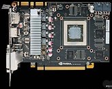
NVIDIA's GeForce GTX 670 Short PCB Pictured Up Close
Thanks to the impressive power-draw and temperature figures its GeForce GTX 680 could come up with, NVIDIA's newest SKU based on the 28 nm GK104 silicon, the GeForce GTX 670, will feature a compact PCB. The reverse side of this PCB was first pictured on a Colorful-branded graphics card. A picture of its obverse side was posted earlier today. In comparison to the GTX 680, the GTX 670 PCB is quite short. The eight GDDR5 memory chips are distributed between both the sides, these chips are wired to the GPU over a 256-bit wide memory interface. The VRM area is pushed towards the front-end of the PCB. It consists of a 4+2 phase design. The card draws power from two 6-pin PCIe power connectors. Display outputs include two dual-link DVI, and one each of HDMI and DisplayPort. There are two SLI bridge connectors, giving it 4-way SLI capability.
Source:
PCinLife

32 Comments on NVIDIA's GeForce GTX 670 Short PCB Pictured Up Close
I couldn't find many pictures but it looks something like this:
This is the perfect budget card(if priced at 300$, but will end up close to 400$)
Suck, Geek, Ugly :shadedshu
What a F$#K PCB Design :banghead:
If your feel alike me, thumb and thanks it Buddy :rockout:
it looks like any other 70 quid card with its cooler off does it not
EDIT: after checking tweaktown preview, seing gtx 670 like 1-2% behind the gtx 680 and 100 bucks cheaper, poor gtx 680, who would buy it? 100 bucks less for 2% less perf? COUNT ME IN FOR A GTX 670!