Sunday, September 2nd 2012

NVIDIA GK106 GPU Pictured, GeForce GTX 660 Benchmarked
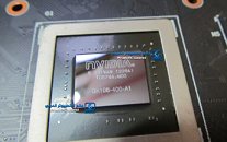
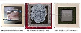
Here are some of the first pictures of NVIDIA's upcoming GK106 silicon, which goes into building the GeForce GTX 660 graphics card. The GK106, built on the 28 nm silicon fab process, is poised to be NVIDIA's newest mainstream-performance chip that succeeds the GF116. The pictures reveal the chip package to be almost as big as the GF116 but smaller than the GK104. This can be attributed to fewer memory I/O pins (192-bit maximum bus width).
The rectangular die of the GK106 appears to have roughly the same area as that of the GF116, but with the higher transistor density of the 28 nm process, one can expect a significantly higher transistor count for the chip. If some of the pictures we're seeing are any indication the GK106 will be extremely energy-efficient, as an unknown graphics card based on it draws power from just one 6-pin power connector.According to the specifications leaked from various sources, some of which include the source of these pictures, the GK106 as GeForce GTX 660 features 960 CUDA cores, 24 ROPs, and a 192-bit wide GDDR5 memory interface, holding 2 GB memory. The card could ship with clock speeds of 980 MHz core, 1033 MHz GPU Boost, and 6.00 GHz memory. At reference speeds and on-spec voltage, the chip could feature a typical power draw of 140W, which explains the need for just one 6-pin power connector.
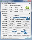
Some of the sources managed to get a GeForce GTX 660 sample running with GeForce 305.27 beta drivers, and put it through 3DMark 11. Below are the GPU-Z screenshot (with some fields blanked out by the source), 3DMark 11 Performance preset and 3DMark 11 eXtreme preset numbers.
Sources:
Arab PC World, 3DCenter.org, VideoCardz
The rectangular die of the GK106 appears to have roughly the same area as that of the GF116, but with the higher transistor density of the 28 nm process, one can expect a significantly higher transistor count for the chip. If some of the pictures we're seeing are any indication the GK106 will be extremely energy-efficient, as an unknown graphics card based on it draws power from just one 6-pin power connector.According to the specifications leaked from various sources, some of which include the source of these pictures, the GK106 as GeForce GTX 660 features 960 CUDA cores, 24 ROPs, and a 192-bit wide GDDR5 memory interface, holding 2 GB memory. The card could ship with clock speeds of 980 MHz core, 1033 MHz GPU Boost, and 6.00 GHz memory. At reference speeds and on-spec voltage, the chip could feature a typical power draw of 140W, which explains the need for just one 6-pin power connector.
Some of the sources managed to get a GeForce GTX 660 sample running with GeForce 305.27 beta drivers, and put it through 3DMark 11. Below are the GPU-Z screenshot (with some fields blanked out by the source), 3DMark 11 Performance preset and 3DMark 11 eXtreme preset numbers.


41 Comments on NVIDIA GK106 GPU Pictured, GeForce GTX 660 Benchmarked
Which ever, looking forward to this chip,anyone wanna place bets on it's performance?
54mm2 differance makes me think (minor) design flaw with GK104 (Boost throttling) or the poor yields they were getting werent panning out with them.
This is the first time I can recall Nvidia has made such a small die-size change from its main line up.
Lots of interesting questions this opens up.
*the other being that GK104 is so much more profitable per wafer and wafers were scarce.
EDIT: Also the size is most definitely 221 mm^2 as reported by GPU-z. User made measures are almost invariably 20-30 mm^2 larger than the actual die size.
GPU-Z added GTX 660 support in v0.6.3 according to the changelogs back in July, so can we assume its already a month and a half behind schedule or somewhere in-between ?
What does your schedule say ?
How do you know GK 106 was redesigned ? Link sources please... I'm sure many here are interested in this information you've obtained ;)
Just doesnt make sense to me that something is on schedule "almost perfectly" when it has to be re-designed. Silly me :)
www.techpowerup.com/reviews/N...GTX_680/2.html
www.nvidia.de/object/geforce-...l#pdpContent=2
The OEM GTX660 has also 6x SMX and 3x Raster-Engines at 1152 Cores 823MHz
and 96 TMU = Tex-Fillrate at 79.0 -- 24x ROP = Pix-Fillr. 19.8
So the 960 Cores 980MHz non-OEM will be at 5x SMX and the same 3x Raster-Engines. 80 TMU Tex-Fillrate ca. at 78.4 -- 24x ROP = Pix-Fillr. 23.5
Right ???
Edit:
The numbers shown in the news-article is reached at about 1070MHz Baseclock.
Nvidia's launch prices are just complete bullshit...
Can't comment on the 650 yet since Wiz does not have any graphs of them yet.
I would be very thankful if you provide an example (a graphics card) which, when used as a point of reference, shows that the current gen is overpriced.
GTX580 launch 500$ - GTX680 launch $500
HD6950 launch $300 - HD7950 launch $450
GTX570 launch $330 - GTX670 launch $400
HD6870 launch 240$ - HD7870 launch $360
GTX560Ti launch 250$ - GTX660Ti launch 300$
August 2010 Gtx460 1GB 256bit about 240$
Jan. 2011 Gtx 560Ti 240$
May 2011 Gtx 560 190$
all at about the Time´s same sweetspot i think
Setting the 6870 compared to the 7870 is kind of unfair because of the "name-degradation-issue" hehe
the 7850 2GB started at about 240$ too.
6970/7970 - +49% price for +43% perf, clearly 7970 is shyte here
580/680 - 0% price for 29%, good
6950/7950 - 50% for 40%, clearly shit
570/670 - 21% for 35%, not bad
6870/7870 - 50% for 47% almost equivalent but no cake
560Ti/660Ti - 20% for 46%, :eek:
So based on my shitty elementary school maths I can conclude that AMD has shit pricing this round, while Nvidia is doing pretty well at the moment. Of course a few months down the road when prices fall things will change a lot etc but for the moment we are not paying more for less other than from AMD, at least according to RRP.
Edit: Its interesting to note that 6970 is just slightly more powerful than 7850, and the launch prices reflect that. Also, 580 is just slightly weaker than 660Ti but the launch prices are extremely different for the two.
Where do I suggest what I say is anything but my opinion? Anyone with half a brain understands that starting a phrase with I'm 99% sure means it's my opinion.
And who said anything about the chip being on schedule or not? You're ridiculous. If the chip was redesigned (1-2 SMX added), and taped out around the time that it was made known that GK104 would be the high-end chip instead of the delayed GK100/110, the release date would be soon enough.
I have to also laugh because of your attempt to connect when the chip is supported by GPUz with my claim of when it (might have) taped out. I think you have no idea of what tape out means, but that shouldn't have been a surprise knowing how many other basic things you don't know.
GK104 taped out ~Aug 2011...
tape out to production of A1 silicon...~6 weeks
testing and validation....~2-3 weeks
tape out to production of A2 silicon...~6 weeks
testing and validation...~2-3 weeks
Commercial production of A2 rev GK104, shipping, binning, packaging...~12 weeks
Assuming that Nvidia got wind of AMD Tahiti's performance around the same time that it was paper launched in late December 2011, that puts it at around the same time as Nvidia testing it's A2 (production) silicon (Hence Nvidia's bullish attitude). At this point, Nvidia would have known from their A2 risk wafers what percentages of full / salvage parts they could expect and their relative performance. I'd say that at this point it was determined that either Nvidia realized that the GK104 was capable of reaching down through the product stack in performance/usable die's sufficiently to satisfy the markets, or that the salvage parts overlapped what the full-die GK106 was capable of. Assume, whatever the reasoning, that the final decision on GK106's makeup was made once A2 GK104 and Tahiti became known quantities, and Nvidia's/TSMC's yields demonstrated that the larger die GK104 was sustainable.
This would equate to a design/redesign between Jan-Apl 2012
tape out to production of A1 silicon...~6 weeks
testing and validation...~2-3 weeks
Commercial production of A1 rev (if the GPU-Z screenshot is correct) GK106, shipping, binning, packaging...~12 weeks
...which takes us to September 2012
Company use this strategy often..
Like I said already, I think both sides are charging too much.
Nice to see fresh silicone coming out from the green team..
i hope they took some credible source this time, because last time, they just took my autocad drawing:
viperxtreme.deviantart.com/art/Some-quick-autocad-stuff-285733301
stole it, then placed their watermark on it then made it as news lolol
www.arabpcworld.com/?p=6498
even some sites followed (if you use google image search)
P.S.
my GTX 460 SE is dying and hope the GTX 660 is well performing and well priced :D
I also see: less IPC, a greater die size, potentially less clockspeed and over-all bandwidth.
7870 still looks nice, considering how often stock or overclocked reviews show it just passing 30 or 60fps in a lot of popular games. This will undoubtedly cause a cut to 229, which I think will be pretty much rock-bottom pricing for that product until we get something new. I won't argue, but I'll guffaw if this is a cent over $200 (I feel proportionally priced correctly vs. 230).
I guess it will be a nice alternative to 7850...faster no doubt and less hassle to overclock...but 1gb versions of that product are probably going to very cheap soon.
I guess the main question will be if it has the balls to be 'just good-enough' for 1080p. Below that will be covered by 7850 for cheaper. 7870 seems up to the task, if only barely...hence I question if this will be a reasonable alternative or not.
I really don't get the 6ghz ram btw...5ghz (stock) should be good-enough for any realistic core clockspeed.