Monday, September 17th 2012

AMD "Oland" Radeon HD 8800 Series SKUs Unveiled
Apparently, launch of AMD's Radeon HD 8800 series is close enough for some sources to come up with specifications. The HD 8800 series, according to one source, is based on a new silicon codenamed "Oland," which is built on the 28 nm process, packing 3.4 billion transistors with around 270 mm² die-area. According to the source, the two HD 8800 series models, the HD 8870 "Oland XT" will up performance per Watt and cost-performance ratios over current HD 7800 series, while maintaining current process technologies.
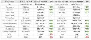
The Radeon HD 8870, according to numbers provided by the source, could offer performance comparable to today's high-end GPUs. The HD 8870 is clocked at 1050 MHz with 1100 MHz PowerTune Boost frequency; while the HD 8850 is clocked at 925 MHz with 975 MHz boost frequency. The memory of both SKUs is clocked at 6.00 GHz, yielding 192 GB/s memory bandwidth. The chips hence have 256-bit wide memory interfaces.Key details such as stream processor, TMU, and ROP counts are excluded, though the source mentions that the HD 8870 provides up to 75% higher single-precision floating point and up to 60% higher double-precision floating point performance over its prdecessor, the HD 7870. The texture fill-rate is up by 65%. The Radeon HD 8850 offers similar increases over its predecessor, the HD 7850. Find them tabled above.
Sources:
Read2ch, VideoCardz
The Radeon HD 8870, according to numbers provided by the source, could offer performance comparable to today's high-end GPUs. The HD 8870 is clocked at 1050 MHz with 1100 MHz PowerTune Boost frequency; while the HD 8850 is clocked at 925 MHz with 975 MHz boost frequency. The memory of both SKUs is clocked at 6.00 GHz, yielding 192 GB/s memory bandwidth. The chips hence have 256-bit wide memory interfaces.Key details such as stream processor, TMU, and ROP counts are excluded, though the source mentions that the HD 8870 provides up to 75% higher single-precision floating point and up to 60% higher double-precision floating point performance over its prdecessor, the HD 7870. The texture fill-rate is up by 65%. The Radeon HD 8850 offers similar increases over its predecessor, the HD 7850. Find them tabled above.

93 Comments on AMD "Oland" Radeon HD 8800 Series SKUs Unveiled
for the ones who dont know, 8 means "rich" in chinese, so people here spend lots of money on car license plates with as many 8s in them as possible, and WD sold an 888GB HDD a while ago if i remember correctly :D
Jokes aside, I was pretty set on a couple 7970s toxic but if specs are already coming out I guess I'll wait :)
If the number are correct - and it looks like someones guesstimate rather than hard numbers- then it's a 112 TMU, 32 ROP part with 2000+ shaders.
Not sure how they arrive at their SP/DP flop numbers unless they are actuals by some measurement. I was under the impression that theoretical FLOP's were measured by- HD 7870 for example:
Core speed * shader count * 2 primatives/clock...which would be 2.56TFLOPS SP, with double precision at 1/16 rate =160GFLOPS
2.25TFlops with 175Watt results in ~12.9GFlops/Watt for the 7870 while the 8870 has:
3.94TFlops with 160Watts powerdraw resulting in 24.6 GFlops/Watt.
Thats practically doubling the Flops/W rating on the same process O.O.
I wonder what breaktrough made that possible.
1792 * 2 * 1.1 GHz = 3,942.4 GFlops/3.9424 TFlops
You got the 112 TMUs and 32 ROPs right.
8850:
1536 * 2 * 0.975 GHz = 2,995.2 GFlops/2.9952 TFlops
96 TMUs and 32 ROPs
8870/8850 = Lower end Tahiti
8850 = 7930 "Tahiti LE" rebranded as Oland Pro
8870 = 7950 "Tahiti Pro" rebranded as Oland XT
Oland dies are probably just 64 GCN * 28 clusters rather than 32 clusters*. With the Venus dies being 80 GCN v2 * 32 clusters for 2,560 GCN cores for Venus XT and 1920-2240 for Venus Pro.
*or similar 128 * 14 / 12
AMD6823.4 = "VENUS PRO"
AMD6821.1 = "VENUS XT"
AMD6820.2 = "VENUS XTX"
Venus XTX = 2x * XT
Venus XT = 2560/160/48
Venus Pro = 2240/140/48
Venus LE(OEM?) = 1920/120/32or48
384 bit or 512 bit
Sadly, Me no likey AMDs drivers so i wont be buying another AMD GPU till they sort that out.
Just waiting to see what Nvidia comes out otherwise 2 670s in SLi scale exceptionally well!
HD 7870 = 1280 * 2 * 1 GHz = 2560 GFlops/2.56 TFlops (as per my original post)- correct?
Yet the graph states 2.25 TFlops :confused:
So I was wondering if the 2.25TF calc for the HD 7870 was also a factor in the 3.94 TF for the new card (i.e. 12%* lower than theoretical). If the Oland is a 1792 shader part, then whomever put the graph together has trouble multiplying three numbers together it would seem...since 3.94TF is a theoretical number, and therefore the theoretical number for the 7870 is 2.56TF - not 2.25
* 1792 shaders * 1.12 = ......... -Which was where the 2k number came in.
I think the actual 7000-Series is completely at the the performance-lowpower 28nm-HPL process.
That could be a reason why the OC on the 7000-series runs earlier to high leakage than NVidia does.
The DP number is correct.
7870 -> 160 FMA GFlops
8870 -> (1792 / 16) * 2 * 1.1 = 246.4 FMA GFlops
www.techpowerup.com/img/12-09-17/78a.jpg