Wednesday, May 20th 2015

AMD "Fiji" HBM Implementation Detailed
Back in 2008, when it looked like NVIDIA owned the GPU market, and AMD seemed lagging behind on the performance and efficiency game, the company sprung a surprise. The company's RV770 silicon, the first GPU to implement GDDR5 memory, trounced NVIDIA's big and inefficient GeForce GTX 200 series, and threw AMD back in the game. GDDR5 helped the company double the memory bandwidth, with lower pin- and memory-chip counts, letting the company and its partners build graphics cards with fewer components, and earn great margins, which the company invested in development of its even better HD 5000 series, that pushed NVIDIA with its comical GeForce GTX 480, to hit its lowest ever in market-share. Could AMD be looking at a similar turnaround this summer?
Since the introduction of its Graphics CoreNext architecture in 2012, AMD has been rather laxed in its product development cycle. The company has come out with a new high-end silicon every 18-24 months, and adopted a strategy of cascading re-branding. The introduction of each new high-end silicon would relegate the existing high-end silicon to the performance segment re-branded, and the existing performance-segment silicon to mid-range, re-branded. While the company could lay out its upcoming Radeon R9 series much in the same way, with the introduction of essentially just one new silicon, "Fiji," it could just prove enough for the company. Much like RV770, "Fiji" is about to bring something that could prove to be a very big feature to the consumer graphics market, stacked high-bandwidth memory (HBM).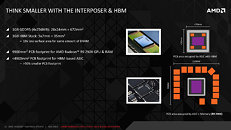
 HBM is being promoted as an upcoming memory standard by JEDEC, and AMD will be the first company to build an ASIC implementing it; with SK Hynix being among the first DRAM makers to build silicon for the standard. HBM is being brought in to address a key problem with GDDR5 - it's not being able to keep up with the growing video memory bandwidth demands of upcoming applications and the GPUs being built to drive them. AMD already has the fastest implementation of GDDR5 on its "Hawaii" silicon, which belts out 320 GB/s of memory bandwidth, but to get there, the company is having to use sixteen memory chips. Placed on a PCB, the ASIC along with the 16 memory chips take up quite a bit of real-estate - 110 mm x 90 mm (99 cm²).
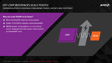
GPU makers haven't managed to take clock speeds of GDDR5 above 1752 MHz (real), and the fact that they're having to use other ways to increase effective bandwidth, such as proprietary lossless memory compression, shows that GDDR5 will fetch diminishing returns for new designs from here on, out. With GDDR5 (or any DRAM standard for that matter), power-consumption doesn't follow a linear curve to support increasing clock speeds. Beyond a point, you need a disproportionate amount of power to support increasing clocks. GDDR5 reached that point. This necessitates HBM.
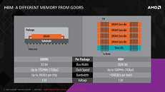
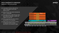
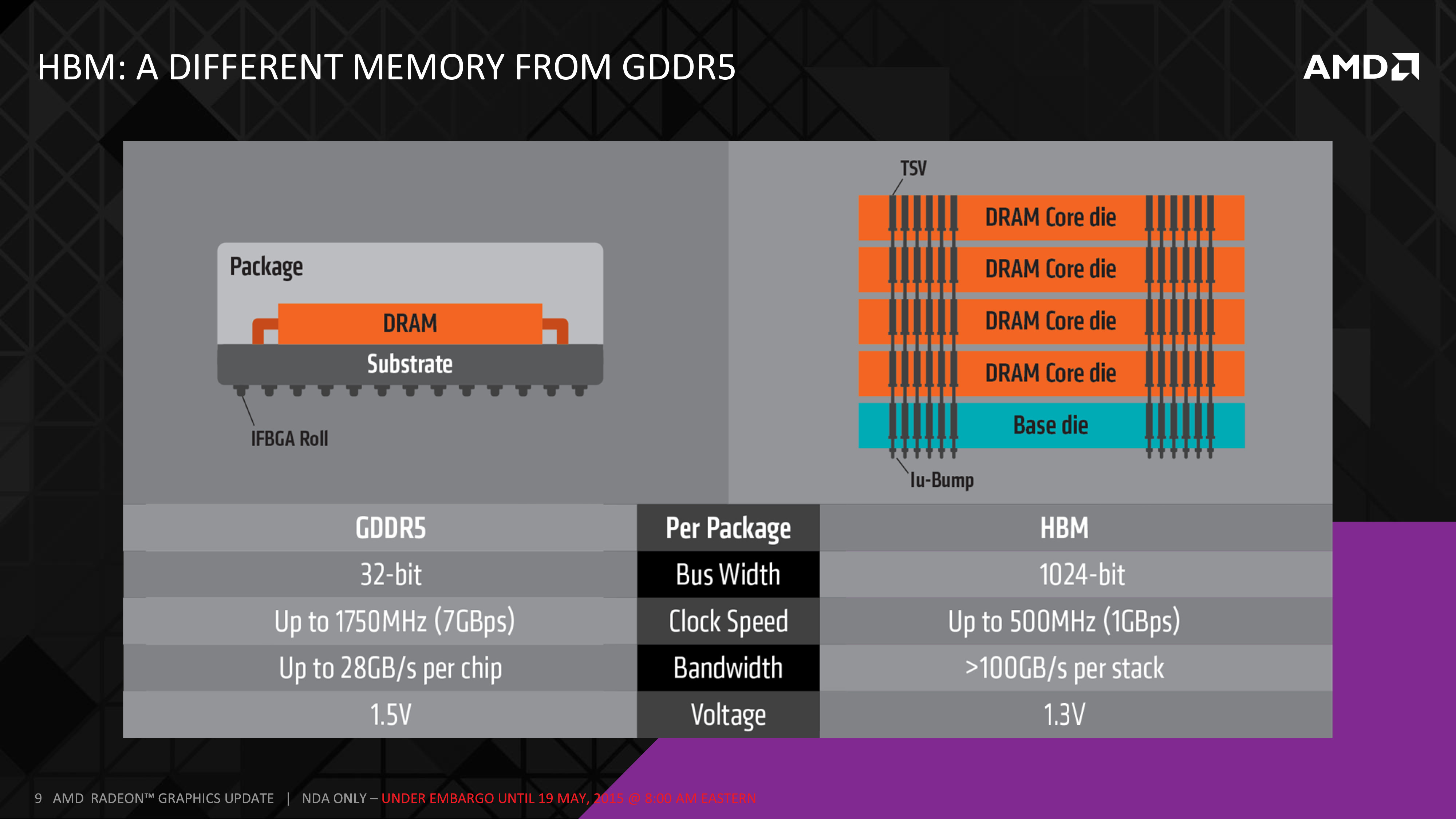
HBM takes a different approach to achieving memory bandwidth than GDDR5. The interface is wider, but with lower clocks (leaving a vast room for future increases in clock speeds). The first generation of HBM, which AMD is implementing on its upcoming high-end graphics cards, pushes just 1 Gbps of data per pin (compared to 7 Gbps on the fastest GDDR5); but features a vast bus width of 1024-bit (compared to just 32-bit per GDDR5 chip). An HBM "chip" is essentially a stack of five dies - a "base die" which holds routing logic, and four DRAM dies, stacked like pancakes (compared to just one DRAM die being bumped out to a BGA package that sits on the PCB, on GDDR5).
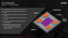
In AMD's implementation of HBM, these "chips" won't be encased into ceramic packages of their own, that sit outside the GPU package, to which it takes intricate wiring along the PCB to reach out to. Instead, HBM chips will be placed right alongside the GPU die, inside the GPU package, on a package substrate AMD calls the "interposer." This is a specially designed substrate layer above the ASIC's own package substrate, which connects the GPU die to the four HBM stacks, with an extremely high density of wiring, that's beyond what conventional multi-layered fiberglass PCBs are capable of. The interposer is perhaps the closest man has come to developing a medulla oblongata.
These stacks, as a result are much closer to the GPU silicon, and the interposer enables extremely high memory bus widths thanks to the density of wiring it can handle. AMD has four such stacks on its upcoming "Fiji" ASIC, resulting in a gargantuan 4096-bit memory bus width. Since HBM pushes lesser data per pin compared to GDDR5, don't expect "Fiji" to have eight times the memory bandwidth as "Hawaii." AMD's flagship Radeon graphics card based on "Fiji" is rumored to feature a memory clock speed of 500 MHz (1 Gbps per pin), which translates in to 512 GB/s of cumulative video memory bandwidth for the GPU, with 128 GB/s per HBM stack. The DRAM voltage is lower, at 1.3V, compared to 1.5V on 7 Gbps GDDR5.
The specifications of the GPU die are constantly being churned up by the rumor mill. Regardless of that, "Fiji" will end up having a lower PCB footprint than "Hawaii." The package will be bigger, but it will no longer be surrounded by memory chips. The PCB look quite different from what we're used to seeing, since the dawn of PC graphics add-in boards. In a way, that's a great thing. AMD retains control over memory, and so its AIB partners can't cheap out with memory chips. We haven't forgotten how some AIBs shortchanged buyers of Radeon R9 290 and R9 290X with cheaper Elpida GDDR5 chips on reference PCBs, even as initial batches (and review samples), came with higher-quality SK Hynix-made ones. Some of the earliest boards with Elpida chips didn't have proper memory timing optimization in the video-BIOS, prompting AIBs to send out BIOS updates. Something like that won't happen with "Fiji," and AIBs are free to cheap out on PCB quality, as the most sensitive wiring (that between the GPU and memory), has now been moved to the GPU package, and its interposer (more quality control in AMD's hands).
So what does this all boil down to? The memory is a more important ingredient in a modern graphics card, than you've been led to believe. The 64-bit computing era is now firmly here, and games are taking advantage of any amount of system- and video-memory you can throw at them. Compound that with DirectX 12, in which the command buffer can take advantage of any number of CPU cores you throw at it, tiled resources, and you're looking at a future that AMD seems to have been preparing for the the past decade (CPUs with a large number of cores, GPUs with extremely high number-crunching parallelism and memory bandwidth). HBM and the way AMD implemented in on its "Fiji" silicon is an important cog in the company's machine. It will offer a brand-new path of bandwidth upscaling through clock speed upscale; and higher energy-efficiency.
It's improbable that AMD would go to such lengths to equip its new high-end silicon, if it wasn't confident of outperforming anything NVIDIA has right now. Likewise, it's improbable that AMD would give a GPU 512 GB/s of memory bandwidth to toy with, if it lacked the chops (number-crunching muscle) to deal with such amount of memory. And this, is what makes "Fiji" a chip to look out for. AMD is expected to tease graphics cards based on "Fiji" at either Computex or E3, with a product launch within June. Let the battle between the Titans and the House of Zeus begin.
Since the introduction of its Graphics CoreNext architecture in 2012, AMD has been rather laxed in its product development cycle. The company has come out with a new high-end silicon every 18-24 months, and adopted a strategy of cascading re-branding. The introduction of each new high-end silicon would relegate the existing high-end silicon to the performance segment re-branded, and the existing performance-segment silicon to mid-range, re-branded. While the company could lay out its upcoming Radeon R9 series much in the same way, with the introduction of essentially just one new silicon, "Fiji," it could just prove enough for the company. Much like RV770, "Fiji" is about to bring something that could prove to be a very big feature to the consumer graphics market, stacked high-bandwidth memory (HBM).

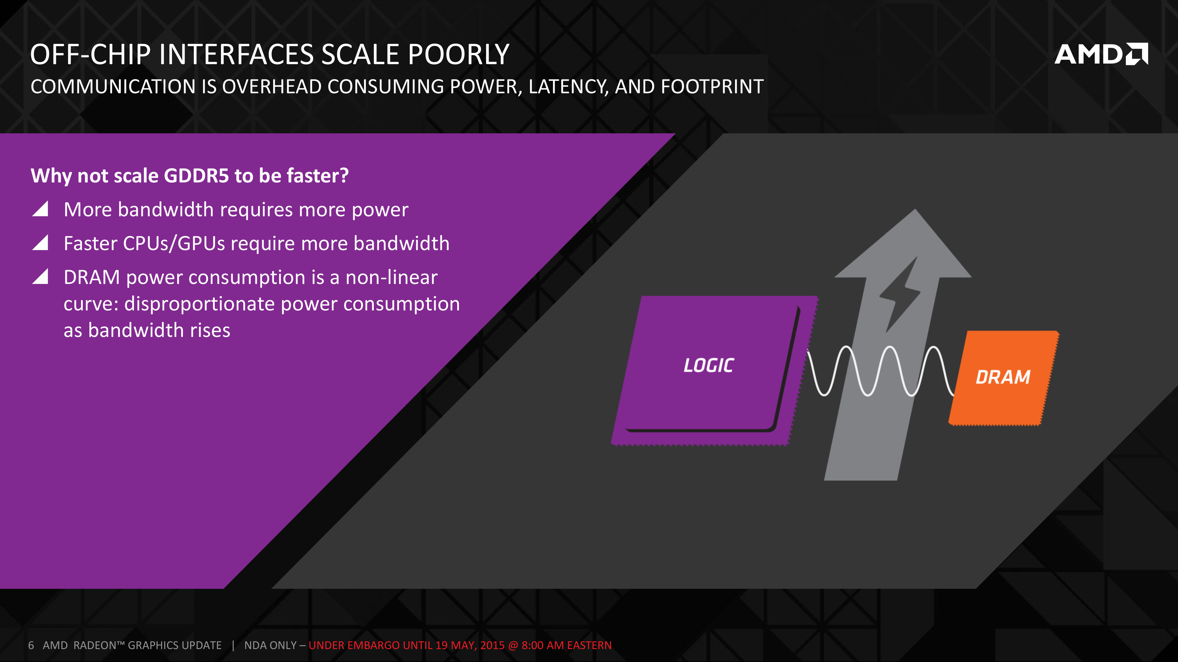


GPU makers haven't managed to take clock speeds of GDDR5 above 1752 MHz (real), and the fact that they're having to use other ways to increase effective bandwidth, such as proprietary lossless memory compression, shows that GDDR5 will fetch diminishing returns for new designs from here on, out. With GDDR5 (or any DRAM standard for that matter), power-consumption doesn't follow a linear curve to support increasing clock speeds. Beyond a point, you need a disproportionate amount of power to support increasing clocks. GDDR5 reached that point. This necessitates HBM.
HBM takes a different approach to achieving memory bandwidth than GDDR5. The interface is wider, but with lower clocks (leaving a vast room for future increases in clock speeds). The first generation of HBM, which AMD is implementing on its upcoming high-end graphics cards, pushes just 1 Gbps of data per pin (compared to 7 Gbps on the fastest GDDR5); but features a vast bus width of 1024-bit (compared to just 32-bit per GDDR5 chip). An HBM "chip" is essentially a stack of five dies - a "base die" which holds routing logic, and four DRAM dies, stacked like pancakes (compared to just one DRAM die being bumped out to a BGA package that sits on the PCB, on GDDR5).
In AMD's implementation of HBM, these "chips" won't be encased into ceramic packages of their own, that sit outside the GPU package, to which it takes intricate wiring along the PCB to reach out to. Instead, HBM chips will be placed right alongside the GPU die, inside the GPU package, on a package substrate AMD calls the "interposer." This is a specially designed substrate layer above the ASIC's own package substrate, which connects the GPU die to the four HBM stacks, with an extremely high density of wiring, that's beyond what conventional multi-layered fiberglass PCBs are capable of. The interposer is perhaps the closest man has come to developing a medulla oblongata.
These stacks, as a result are much closer to the GPU silicon, and the interposer enables extremely high memory bus widths thanks to the density of wiring it can handle. AMD has four such stacks on its upcoming "Fiji" ASIC, resulting in a gargantuan 4096-bit memory bus width. Since HBM pushes lesser data per pin compared to GDDR5, don't expect "Fiji" to have eight times the memory bandwidth as "Hawaii." AMD's flagship Radeon graphics card based on "Fiji" is rumored to feature a memory clock speed of 500 MHz (1 Gbps per pin), which translates in to 512 GB/s of cumulative video memory bandwidth for the GPU, with 128 GB/s per HBM stack. The DRAM voltage is lower, at 1.3V, compared to 1.5V on 7 Gbps GDDR5.
The specifications of the GPU die are constantly being churned up by the rumor mill. Regardless of that, "Fiji" will end up having a lower PCB footprint than "Hawaii." The package will be bigger, but it will no longer be surrounded by memory chips. The PCB look quite different from what we're used to seeing, since the dawn of PC graphics add-in boards. In a way, that's a great thing. AMD retains control over memory, and so its AIB partners can't cheap out with memory chips. We haven't forgotten how some AIBs shortchanged buyers of Radeon R9 290 and R9 290X with cheaper Elpida GDDR5 chips on reference PCBs, even as initial batches (and review samples), came with higher-quality SK Hynix-made ones. Some of the earliest boards with Elpida chips didn't have proper memory timing optimization in the video-BIOS, prompting AIBs to send out BIOS updates. Something like that won't happen with "Fiji," and AIBs are free to cheap out on PCB quality, as the most sensitive wiring (that between the GPU and memory), has now been moved to the GPU package, and its interposer (more quality control in AMD's hands).
So what does this all boil down to? The memory is a more important ingredient in a modern graphics card, than you've been led to believe. The 64-bit computing era is now firmly here, and games are taking advantage of any amount of system- and video-memory you can throw at them. Compound that with DirectX 12, in which the command buffer can take advantage of any number of CPU cores you throw at it, tiled resources, and you're looking at a future that AMD seems to have been preparing for the the past decade (CPUs with a large number of cores, GPUs with extremely high number-crunching parallelism and memory bandwidth). HBM and the way AMD implemented in on its "Fiji" silicon is an important cog in the company's machine. It will offer a brand-new path of bandwidth upscaling through clock speed upscale; and higher energy-efficiency.
It's improbable that AMD would go to such lengths to equip its new high-end silicon, if it wasn't confident of outperforming anything NVIDIA has right now. Likewise, it's improbable that AMD would give a GPU 512 GB/s of memory bandwidth to toy with, if it lacked the chops (number-crunching muscle) to deal with such amount of memory. And this, is what makes "Fiji" a chip to look out for. AMD is expected to tease graphics cards based on "Fiji" at either Computex or E3, with a product launch within June. Let the battle between the Titans and the House of Zeus begin.
29 Comments on AMD "Fiji" HBM Implementation Detailed
As to the budget/low-end yes AMD has way too much confusion in that range! They need just a budget/basic that's more a repair or diagnosis type card even if it a from two process’ ago (6450). Then as "low-end"; a nice step above a common iGPU in mainstream CPU, good HTPC and low power. Ultimately with AMD that “Low-End” should be intended pair up with APU's to really provide "Dual Graphics" (for once) that offers enhanced "entry gaming" (gets you into 1080p) when paired together. That really needs to be a compelling straight-forward upgrade, for APU OEM boxes. AMD should be off-loading APU’s in the market for margins even if razor thin, and really work to pick up that discrete card sale of $60 after.
After that there's:
Entry: Adolescence-Early teens, $80-120 works with OEM 300W PSU
Mainstream: Teen's (6-10 hrs/wk) strong 1080p, $130-200
Gamer: (12-25 hrs/wk) High settings 1080p, able to provide >med. 1440p, ≥500W PSU $230-500
Enthusiast: Whatever...
So you really end up designing a chip for each of those 4 segments, and being there's the full-fledged and a least one gelding, quickly you could see at minimum 6 cards, if you get lucky and the cost/perf/power works to transfer to the lower level. It's nice if your gelding parts can become mobile/OEM discrete, but then such market don't gobble the volume of chips that you amass if doing really great on the retail side.
It’s more of a juggling act between what engineering finally provides, where the competition falls perf/$, how long can you bin/hold geldings and will there be a good opening to exploit if you sit on them. It’s tougher than folk think, especially if you’re the underdog and every dollar counts.
I was thinking about replacing my 6870s, but I think I'm going to hold on for a little bit for obvious reasons. :)
Really nice featurette in general and pretty notable comments on the topic. Despite being in the "green camp" almost all my life so far, I must say I am intrigued about what AMD is cooking. I don't know if I will jump on the wagon, but I'd like them to have something low-profile-sized with DDR5 for around a 100 bucks that's actually better than GT740/640 for my portable RIG.