News Posts matching #JEDEC

Return to Keyword Browsing

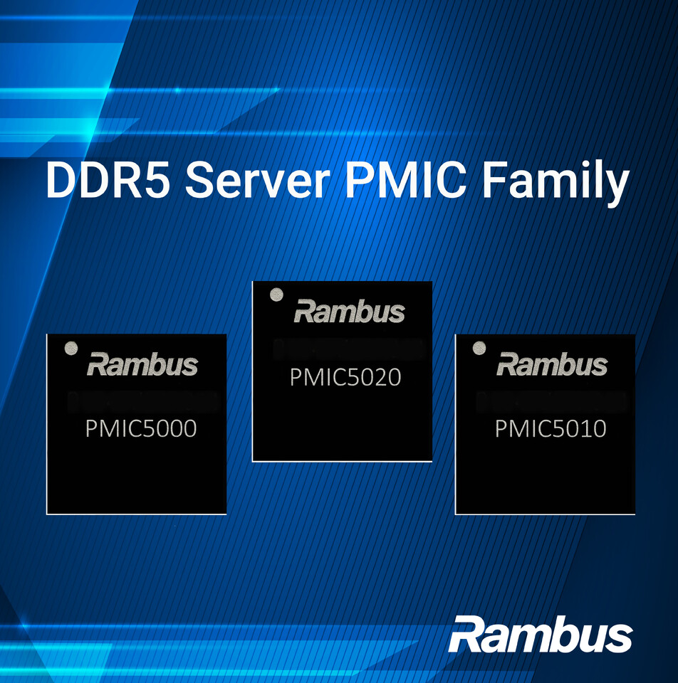
Rambus Expands Chipset for Advanced Data Center Memory Modules with DDR5 Server PMICs

Rambus Inc. (NASDAQ: RMBS), a premier chip and silicon IP provider making data faster and safer, today announced the availability of its new family of state-of-the-art DDR5 server Power Management ICs (PMICs), including an industry-leading extreme current device for high-performance applications. With this new family of server PMICs, Rambus offers module manufacturers a complete DDR5 RDIMM memory interface chipset supporting a broad range of data center use cases.

"Advanced data center workloads like generative AI require the highest bandwidth and capacity server RDIMMs tailored to meet ever-increasing memory needs of a growing data pipeline," said Sean Fan, chief operating officer at Rambus. "With the addition of this new family of server PMICs, we expand our foundational technology and offer customers a comprehensive memory interface chipset that supports multiple DDR5 server platform generations."

JEDEC Updates DDR5 Specification for Increased Security Against Rowhammer Attacks, New DDR5-8800 Reference Speed

JEDEC Solid State Technology Association, the global leader in standards development for the microelectronics industry, today announced publication of the JESD79-5C DDR5 SDRAM standard. This important update to the JEDEC DDR5 SDRAM standard includes features designed to improve reliability and security and enhance performance in a wide range of applications from high-performance servers to emerging technologies such as AI and machine learning. JESD79-5C is now available for download from the JEDEC website.

JESD79-5C introduces an innovative solution to improve DRAM data integrity called Per-Row Activation Counting (PRAC). PRAC precisely counts DRAM activations on a wordline granularity. When PRAC-enabled DRAM detects an excessive number of activations, it alerts the system to pause traffic and to designate time for mitigative measures. These interrelated actions underpin PRAC's ability to provide a fundamentally accurate and predictable approach for addressing data integrity challenges through close coordination between the DRAM and the system.

CORSAIR Enters DDR5 Workstation Market with WS DDR5 RDIMM ECC Memory Kits

Corsair today announced it is entering the DDR5 Workstation market with the introduction of a range of WS DDR5 RDIMM memory kits. Engineered to offer uncompromising performance and reliability, these ECC RDIMM kits redefine the capabilities of the newest workstations, and are compatible with the latest 4th Gen Intel Xeon and AMD Ryzen Threadripper 7000 processors.

This new range of memory kits boasts capacities of up to 256 GB, setting a new standard for memory-intensive tasks such as high-resolution media editing, 3D rendering, and AI training. Rigorously tested and carefully screened, these modules surpass JEDEC specifications with tighter timings and higher frequencies, ensuring optimal performance for the most demanding workloads.

Montage Technology Pioneers the Trial Production of DDR5 CKDs

Montage Technology, a leading data processing and interconnect IC company, today announced that it has taken the lead in the trial production of 1st-generation DDR5 Clock Driver (CKD) chips for next-generation client memory. This new product aims to enhance the speed and stability of memory data access to match the ever-increasing CPU operating speed and performance.

Previously, clock driver functionality was integrated into the Registering Clock Driver (RCD) chips used on server RDIMM or LRDIMM modules, not deployed to the PCs. In the DDR5 era, as data rates climb 6400 MT/s and above, the clock driver has emerged as an indispensable component for client memory.

Introspect Technology Ships World's First GDDR7 Memory Test System

Introspect Technology, a JEDEC member and a leading manufacturer of test and measurement instruments, announced today that it has shipped the M5512 GDDR7 Memory Test System, the world's first commercial solution for testing JEDEC's newly minted JESD239 Graphics Double Data Rate (GDDR7) SGRAM specification. This category-creating solution enables graphics memory engineers, GPU design engineers, product engineers in both memory and GPU spaces, and system integrators to rapidly bring up new GDDR7 memory devices, debug protocol errors, characterize signal integrity, and perform detailed memory read/write functional stress testing without requiring any other tool.

The GDDR7 specification is the latest industry standard that is aimed at the creation of high-bandwidth and high-capacity memory implementations for graphics processing, artificial intelligence (AI), and AI-intensive networking. Featuring pulse-amplitude modulation (PAM) and an improved signal to noise ratio compared to other PAM4 standards used in networking, the GDDR7 PAM3 modulation technology achieves greater power-efficiency while significantly increasing data transmission bandwidth over constrained electrical channels.

Samsung Shows Off 32 Gbps GDDR7 Memory at GTC

Samsung Electronics showed off its latest graphics memory innovations at GTC, with an exhibit of its new 32 Gbps GDDR7 memory chip. The chip is designed to power the next generation of consumer and professional graphics cards, and some models of NVIDIA's GeForce RTX "Blackwell" generation are expected to implement GDDR7. The chip Samsung showed off at GTC is of the highly relevant 16 Gbit density (2 GB). This is important, as NVIDIA is rumored to keep graphics card memory sizes largely similar to where they currently are, while only focusing on increasing memory speeds.

The Samsung GDDR7 chip shown is capable of its 32 Gbps speed at a DRAM voltage of just 1.1 V, which beats the 1.2 V that's part of JEDEC's GDDR7 specification, which along with other power management innovations specific to Samsung, translates to a 20% improvement in energy efficiency. Although this chip is capable of 32 Gbps, NVIDIA isn't expected to give its first GeForce RTX "Blackwell" graphics cards that speed, and the first SKUs are expected to ship with 28 Gbps GDDR7 memory speeds, which means NVIDIA could run this Samsung chip at a slightly lower voltage, or with better timings. Samsung also made some innovations with the package substrate, which decreases thermal resistance by 70% compared to its GDDR6 chips. Both NVIDIA and AMD are expected to launch their first discrete GPUs implementing GDDR7, in the second half of 2024.

JEDEC Agrees to Relax HBM4 Package Thickness

JEDEC is currently presiding over standards for 6th generation high bandwidth memory (AKA HBM4)—the 12 and 16-layer DRAM designs are expected to reach mass production status in 2026. According to a ZDNET South Korea report, involved manufacturers are deliberating over HBM4 package thicknesses—allegedly, decision makers have settled on 775 micrometers (μm). This is thicker than the previous generation's measurement of 720 micrometers (μm). Samsung Electronics, SK Hynix and Micron are exploring "hybrid bonding," a new packaging technology—where onboard chips and wafers are linked directly to each other. Hybrid bonding is expected to be quite expensive to implement, so memory makers are carefully considering whether HBM4 warrants its usage.

ZDNET believes that JEDEC's agreement—settling on 775 micrometers (μm) for 12-layer and 16-layer stacked HBM4—could have: "a significant impact on the future packaging investment trends of major memory manufacturers. These companies have been preparing a new packaging technology, hybrid bonding, keeping in mind the possibility that the package thickness of HBM4 will be limited to 720 micrometers. However, if the package thickness is adjusted to 775 micrometers, 16-layer DRAM stacking HBM4 can be sufficiently implemented using existing bonding technology." A revised schedule could delay the rollout of hybrid bonding—perhaps pushed back to coincide with a launch of seventh generation HBM. The report posits that Samsung Electronics, SK Hynix and Micron memory engineers are about to focus on the upgrading of existing bonding technologies.

Silicon Motion Unveils 6nm UFS 4.0 Controller for AI Smartphones, Edge Computing and Automotive Applications

Silicon Motion Technology Corporation ("Silicon Motion"), a global leader in designing and marketing NAND flash controllers for solid state storage devices, today introduced its UFS (Universal Flash Storage) 4.0 controller, the SM2756, as the flagship of the industry's broadest merchant portfolio of UFS controller solutions for the growing requirements of AI-powered smartphones as well as other high-performance applications including automotive and edge computing. The company also added a new, second generation SM2753 UFS 3.1 controller to broaden its portfolio of controllers now supporting UFS 4.0 to UFS 2.2 standards. Silicon Motion's UFS portfolio delivers high-performance and low power embedded storage for flagship to mainstream and value mobile and computing devices, supporting the broadest range of NAND flash, including next-generation high speed 3D TLC and QLC NAND.

The new SM2756 UFS 4.0 controller solution is the world's most advanced controller, built on leading 6 nm EUV technology and using MIPI M-PHY low-power architecture, providing the right balance of high performance and power efficiency to enable the all day computing needs of today's premium and AI mobile devices. The SM2756 achieves sequential read performance exceeding 4,300 MB/s and sequential write speeds of over 4,000 MB/s and supports the broadest range of 3D TLC and QLC NAND flash with densities of up to 2 TB.

JEDEC Reportedly Finalizing LPDDR6 Standard for Mobile Platforms

JEDEC is expected to announce a next-gen low-power RAM memory (LPDDR) standard specification by the third quarter of this year. Earlier today, smartphone technology watcher—Revegnus—highlighted insider information disclosed within an ETnews article. The International Semiconductor Standards Organization (JEDEC) has recently concluded negotiations regarding "next-generation mobile RAM standards"—the report posits that: "more than 60 people from memory, system semiconductor, and design asset (IP) companies participated" in a Lisbon, Portugal-situated meeting. A quoted participant stated (to ETnews): "We have held various discussions to confirm the LPDDR6 standard specification...(Details) will be released in the third quarter of this year."

The current generation LPDDR5 standard was secured back in February 2019—noted improvements included 50% performance and 30% power efficiency jumps over LPDDR4. Samsung Electronics and SK Hynix are in the process of mass-producing incremental improvements—in the form of LPDDR5X and LPDDR5T. A second source stated: "Technology development and standard discussions are taking place in a way to minimize power consumption, which increases along with the increase in data processing." A full-fledged successor is tasked with further enhancing data processing performance. Industry figures anticipate that LPDDR6 will greatly assist in an industry-wide push for "on-device AI" processing. They reckon that "large-scale AI calculations" will become the norm on smartphones, laptops, and tablet PCs. Revegnus has heard (fanciful) whispers about a potential 2024 rollout: "support may be available starting with Qualcomm's Snapdragon 8 Gen 4, expected to be released as early as the second half of this year." Sensible predictions point to possible commercialization in late 2025, or early 2026.

NVIDIA RTX 50-series "GB20X" GPU Memory Interface Details Leak Out

Earlier in the week it was revealed that NVIDIA had distributed next-gen AI GPUs to its most important ecosystem partners and customers—Dell's CEO expressed enthusiasm with his discussion of "Blackwell" B100 and B200 evaluation samples. Team Green's next-gen family of gaming GPUs have received less media attention in early 2024—a mid-February TPU report pointed to a rumored PCIe 6.0 CEM specification for upcoming RTX 50-series cards, but leaks have become uncommon since late last year. Top technology tipster, kopite7kimi, has broken the relative silence on Blackwell's gaming configurations—an early hours tweet posits a slightly underwhelming scenario: "although I still have fantasies about 512 bit, the memory interface configuration of GB20x is not much different from that of AD10x."

Past disclosures have hinted about next-gen NVIDIA gaming GPUs sporting memory interface configurations comparable to the current crop of "Ada Lovelace" models. The latest batch of insider information suggests that Team Green's next flagship GeForce RTX GPU—GB202—will stick with a 384-bit memory bus. The beefiest current-gen GPU AD102—as featured in GeForce RTX 4090 graphics cards—is specced with a 384-bit interface. A significant upgrade for GeForce RTX 50xx cards could arrive with a step-up to next-gen GDDR7 memory—kopite7kimi reckons that top GPU designers will stick with 16 Gbit memory chip densities (2 GB). JEDEC officially announced its "GDDR7 Graphics Memory Standard" a couple of days ago. VideoCardz has kindly assembled the latest batch of insider info into a cross-generation comparison table (see below).

First GPUs Implementing GDDR7 Memory Could Stick with 16 Gbit Chips, 24 Gbit Possible

Some of the first gaming GPUs that implement the next-generation GDDR7 memory standard, will stick to 16 Gbit memory chip densities (2 GB), according to kopite7kimi, a reliable source with NVIDIA GeForce leaks. 16 Gbit is what is standard for the current RTX 40-series graphics cards, which ensures that a GPU with 256-bit memory bus gets 16 GB of video memory; the ones with 192-bit get 12 GB; and the ones with 128-bit get 8 GB. The flagship RTX 4090 uses twelve of these chips over its 384-bit memory bus for 24 GB.

Kopite7kimi's leak could have a different connotation, that much like the RTX 30-series "Ampere" and RTX 40-series "Ada," NVIDIA might not use JEDEC-standard GDDR7 on all product segments, and might co-engineer an exclusive standard with a DRAM company with memory bus signaling and power management technologies most optimal to its graphics architecture. It co-developed the GDDR6X with Micron Technology to do exactly this. GDDR7 comes with data-rates as high as 32 Gbps, which will be the top speed for the first round of GDDR7 chips that come out toward the end of 2024, heading into 2025. The second round of GDDR7 chips slated for late-2025 going into 2026, could go as fast as 36 Gbps. This is similar to how the first GDDR6 chips were 14-16 Gbps, and the next round did 18-20 Gbps.

JEDEC Publishes GDDR7 Graphics Memory Standard

JEDEC Solid State Technology Association, the global leader in the development of standards for the microelectronics industry, is pleased to announce the publication of JESD239 Graphics Double Data Rate (GDDR7) SGRAM. This groundbreaking new memory standard is available for free download from the JEDEC website. JESD239 GDDR7 offers double the bandwidth over GDDR6, reaching up to 192 GB/s per device, and is poised to meet the escalating demand for more memory bandwidth in graphics, gaming, compute, networking and AI applications.

JESD239 GDDR7 is the first JEDEC standard DRAM to use the Pulse Amplitude Modulation (PAM) interface for high frequency operations. Its PAM3 interface improves the signal to noise ratio (SNR) for high frequency operation while enhancing energy efficiency. By using 3 levels (+1, 0, -1) to transmit 3 bits over 2-cycles versus the traditional NRZ (non-return-to-zero) interface transmitting 2 bits over 2-cycles, PAM3 offers higher data transmission rate per cycle resulting in improved performance.

Intel CEO Pat Gelsinger Receives 2024 Distinguished Executive Leadership Award from JEDEC Board

The JEDEC Board of Directors presented its prestigious 2024 Distinguished Executive Leadership Award to Intel CEO, Pat Gelsinger, in a ceremony held at Intel's offices in Santa Clara, CA earlier this month. This award stands as JEDEC's highest honor and recognizes the most distinguished senior executives in the electronics industry who promote and support the advancement of JEDEC standards.

"Throughout Pat Gelsinger's distinguished career, he has consistently championed the development of open standards, as evidenced by Intel's contributions in this domain. Under his leadership, Intel has made a tremendous impact on many groundbreaking memory and IO technologies in JEDEC," said Mian Quddus, JEDEC Board of Directors Chairman. He added, "JEDEC is grateful for his invaluable support and that of the Intel team."

Kioxia Introduces Industry's First UFS Ver. 4.0 Embedded Flash Memory Devices for Automotive Applications

Kioxia Corporation, a world leader in memory solutions, today announced sampling of the industry's first Universal Flash Storage (UFS) Ver. 4.0 embedded flash memory devices designed for automotive applications. These new, higher performing devices deliver fast embedded storage transfer speeds in a small package size and are targeted to a variety of next-generation automotive applications, including telematics, infotainment systems and ADAS. The improved performance] of UFS products from Kioxia - including approximately +100% for sequential read speed and approximately +40% for sequential write speed - enables these applications to take advantage of 5G's connectivity benefits, leading to faster system startup times and a better user experience.

The first to introduce UFS technology, Kioxia continues to move the technology forward. Its new UFS Ver. 4.0 devices integrate the company's innovative BiCS FLASH 3D flash memory and a controller in a JEDEC-standard package. UFS 4.0 incorporates MIPI M-PHY 5.0 and UniPro 2.0 and supports theoretical interface speeds of up to 23.2 Gbps per lane or 46.4 Gbps per device. UFS 4.0 is backward compatible with UFS 3.1.

SK Hynix Throws a Jab: CAMM is Coming to Desktop PCs

In a surprising turn of events, SK Hynix has hinted at the possibility of the Compression Attached Memory Module (CAMM) standard, initially designed for laptops, being introduced to desktop PCs. This revelation came from a comment made by an SK Hynix representative at the CES 2024 in Las Vegas for the Korean tech media ITSubIssub. According to the SK Hynix representative, the first implementation is underway, but there are no specific details. CAMM, an innovative memory standard developed by Dell in 2022, was certified to replace SO-DIMM as the official standard for laptop memory. However, the transition to desktop PCs could significantly disrupt the desktop memory market. The CAMM modules, unlike the vertical DRAM sticks currently in use, are horizontal and are screwed into a socket. This design change would necessitate a complete overhaul of the desktop motherboard layout.

The thin, flat design of the CAMM modules could also limit the number that can be installed on an ATX board. However, the desktop version of the standard CAMM2 was announced by JEDEC just a month ago. It is designed for DDR5 memory, but it is expected to become mainstream with the introduction of DDR6 around 2025. While CAMM allows for higher speeds and densities for mobile memory, its advantages for desktops over traditional memory sticks are yet to be fully understood. Although low-power CAMM modules could offer energy savings, this is typically more relevant for mobile devices than desktops. As we move towards DDR6 and DDR7, more information about CAMM for desktops will be needed to understand its potential benefits. JEDEC's official words on the new standard indicate that "DDR5 CAMM2s are intended for performance notebooks and mainstream desktops, while LPDDR5/5X CAMM2s target a broader range of notebooks and certain server market segments." So, we can expect to see CAMM2 in both desktops and some server applications.

Patriot Memory at 2024 CES: 14GB/s Gen 5 SSDs, USB4 Prototypes, DDR5 Memory with CKD

Patriot Memory brought their latest ware to the 2024 International CES that use recent advancements in tech on both the SSD and memory fronts. On the SSD front, this year sees 14 GB/s capable PCIe Gen 5 NVMe SSDs thanks to Phison's E26 Max14um controller; and a new crop of USB4 portable SSDs; while the memory front sees DDR5 speeds go far north of DDR5-6000, thanks to on-module CKDs. Patriot showed us examples of each.

First up, there's the Patriot Viper PV573 Gen 5 NVMe SSD. This thing comes in capacities of up to 4 TB, and combines a Phison E26 Max14um controller with Micron's latest B58R TLC NAND flash chips that offer 2400 MT/s per flash channel. The controller also gets some incremental thermal optimizations, which means the cooling solution for the PV573 is a 16.5 mm-tall fan-heatsink. The drive offers up to 14 GB/s sequential reads, with up to 12 GB/s sequential writes. There's also a slightly de-rated version of this drive, the Viper PV553, which has the same combination of controller and NAND flash, but with transfer speeds of up to 12.4 GB/s reads, with up to 11.8 GB/s writes.

Montage Technology Introduces 4th-Gen DDR5 RCDs Enabling Data Rates up to 7200 MT/s

Montage Technology, a leading data processing and interconnect IC company, today introduced its 4th-gen DDR5 Registering Clock Driver (RCD), also called DDR5 RCD04, to the industry. Designed for DDR5 RDIMM memory modules, this chip supports blazing-fast data rates up to 7200 MT/s, a 50% increase over the 1st-gen DDR5 RCDs.

As a leader in memory interface technologies, Montage has led the development of JEDEC standards for DDR5 RCD chips and sustains high R&D investments to enable continuous product iterations and upgrades. Since debuting its 1st-gen DDR5 memory interface and memory module supporting chips in 2021, the company successfully released the second and third generation DDR5 RCD chips in 2022 and 2023 respectively.

JEDEC Publishes New CAMM2 Memory Module Standard

JEDEC Solid State Technology Association, the global leader in the development of standards for the microelectronics industry, today announced the publication of JESD318: Compression Attached Memory Module (CAMM2) Common Standard. This groundbreaking standard defines the electrical and mechanical requirements for both Double Data Rate, Synchronous DRAM Compression-Attached Memory Modules (DDR5 SDRAM CAMM2s) and Low Power Double Data Rate, Synchronous DRAM Compression-Attached Memory Modules (LPDDR5/5X SDRAM CAMM2s) in a single, comprehensive document. JESD318 CAMM2 is available for download from the JEDEC website.

DDR5 and LPDDR5/5X CAMM2s cater to distinct use cases. DDR5 CAMM2s are intended for performance notebooks and mainstream desktops, while LPDDR5/5X CAMM2s target a broader range of notebooks and certain server market segments.

SK Hynix Announces Production LPDDR5T, World's Fastest Mobile Memory Standard

SK hynix Inc. announced today that it has started supplying its customers with 16 gigabyte (GB) packages of Low Power Double Data Rate 5 Turbo (LPDDR5T), the fastest mobile DRAM available today that can transfer 9.6 gigabits per second (Gbps). Since the successful development of its LPDDR5T in January, SK hynix has been preparing to commercialize the product by conducting performance verification with global mobile application processor (AP) manufacturers.

SK hynix explained that LPDDR5T is the optimal memory to maximize the performance of smartphones, with the highest speed ever achieved. The company also emphasized that it would continue to expand the application range of this product and lead the generation shift in the mobile DRAM sector. The LPDDR5T 16 GB package operates in the ultra-low voltage range of 1.01 to 1.12 V set by the Joint Electron Device Engineering Council (JEDEC), and can process 77 GB of data per second, which is equivalent to transferring 15 full high-definition (FHD) movies in one second.

Micron Announces 128GB DRAM Low-Latency, High-Capacity RDIMMs

Micron Technology, Inc. (Nasdaq: MU), today demonstrated its industry leadership by announcing its 32Gb monolithic die-based 128 GB DDR5 RDIMM memory featuring best-in-class performance of up to 8000 MT/s to support data center workloads today and into the future. These high-capacity, high-speed memory modules are engineered to meet the performance and data-handling needs of a wide range of mission-critical applications in data center and cloud environments, including artificial intelligence (AI), in-memory databases (IMDBs) and efficient processing for multithreaded, multicore count general compute workloads.

Powered by Micron's industry-leading 1β (1-beta) technology, the 32Gb DDR5 DRAM die-based 128 GB DDR5 RDIMM memory delivers the following enhancements over competitive 3DS through-silicon via (TSV) products:
  • more than 45% improved bit density
  • up to 24% improved energy efficiency
  • up to 16% lower latency
  • up to a 28% improvement in AI training performance

SK Hynix's LPDDR5T, World's Fastest Mobile DRAM, Completes Compatibility Validation with Qualcomm

SK hynix Inc. announced today that it has started commercialization of the LPDDR5T (Low Power Double Data Rate 5 Turbo), the world's fastest DRAM for mobile with 9.6 Gbps speed. The company said that it has obtained the validation that the LPDDR5T is compatible with Qualcomm Technologies' new Snapdragon 8 Gen 3 Mobile Platform, marking the industry's first case for such product to be verified by the U.S. company.

SK hynix has proceeded with the compatibility validation of the LPDDR5T, following the completion of the development in January, with support from Qualcomm Technologies. The completion of the process means that it is compatible with Snapdragon 8 Gen 3. With the validation process with Qualcomm Technologies, a leader in wireless telecommunication products and services, and other major mobile AP (Application Processor) providers successfully completed, SK hynix expects the range of the LPDDR5T adoption to grow rapidly.

JEDEC and Open Compute Project Foundation Pave the Way for a New Era of Chiplet Innovation

In an extraordinary leap forward for the chiplet industry, the groundbreaking collaboration between the Open Compute Project Foundation (OCP) and JEDEC is set to usher in a new era of innovation. By merging the capabilities and open standards of OCP's Chiplet Data Extensible Markup Language (CDXML) and JEDEC's JEP30 PartModel Guidelines, this partnership, initiated in late 2022, promises to revolutionize chiplet design, manufacturing and integration. The result will be a unified structure that supports both chiplets and general electronic parts within the overarching purview of JEDEC.

In a significant development, the integration of OCP CDXML into JEP30 has reached a critical milestone, enabling chiplet builders to provide standardized chiplet part descriptions to their customers electronically. This advancement opens the door to automating System in Package (SiP) design and assembly using chiplets. The chiplet descriptions encompass crucial information for SiP builders, including thermal properties, physical and mechanical requirements, behavior specifications, power and signal integrity properties, testing in-package and security parameters.

Kioxia Introduces Next Generation e-MMC Ver. 5.1-Compliant Embedded Flash Memory

Kioxia Corporation, a world leader in memory solutions, today announced sampling of new, higher performing JEDEC e-MMC Ver. 5.1-compliant embedded flash memory products for consumer applications. The new products integrate a newer version of the company's BiCS FLASH 3D flash memory and a controller in a single package, reducing processor workload and improving ease of use. Both 64 and 128 gigabytes (GB) products will be available.

As the market continues to shift to UFS, there are cases where e-MMC may still be used. This includes consumer products with mid-range storage requirements such as tablets, personal computers, point of sale devices and other portable handheld devices, as well as smart TVs and smart NICs. Kioxia continues to reinforce its market-leading position by delivering a broad, high-performance product lineup and expanding the available options for these applications.

Crucial Launches DDR5 6000 MHz Pro DIMMs

When Crucial cancelled its Ballistix gaming brand, it was unclear if the company would launch higher-end products in the future, although the company never said it wouldn't. Back in May of this year, Crucial launched its Pro series of memory, which was not exactly pro, at least not for the readership here which is used to an entirely different level of RAM. This was largely due to Crucial sticking to JEDEC spec, even though the company did launch some DDR5 5600 MHz modules.

Now—some six months later—it appears that Crucial is getting ready to deliver some higher performance modules with its new DDR5 6000 MHz modules, although at launch, they will only be available in a kit of two 24 GB modules. Although Crucial claims JEDEC spec, the 48-48-48 timings appear to either be slightly tighter than the original JEDEC spec, or JEDEC has updated the specs since they were announced. Although nothing about these modules screams high-end or pro, there's one thing that makes these stand out against the competition, they operate at 6000 MHz using only 1.1 Volt, whereas most 6000 MHz DIMMs on the market today, operate at 1.35 Volt higher. In addition to that, as these are JEDEC spec DIMMs, there's no need to enable XMP/EXPO settings to make them work at 6000 MHz, which could be a benefit to some. There might be some potential for tweaking these modules as well, something we'll have to wait for reviews to find out about. Crucial is asking for US$166.99 for the 48 GB kit, which puts them at a price disadvantage compared to its competitors, as you can get a similar kit for as little as $115 or possibly even less.

SK hynix Starts Mass Production of Industry's First 24GB LPDDR5X DRAM

SK hynix Inc. (or "the company", www.skhynix.com) announced today that it has begun supplying the industry's first 24-gigabyte (GB) Low Power Double Data Rate 5X (LPDDR5X) mobile DRAM package to its customers, following the mass production of LPDDR5X in November 2022. SK hynix, in January, developed LPDDR5T, which is an upgraded product of LPDDR5X prior to the development of the 8th generation LPDDR6, and is currently processing customer validation.

"The company integrated the High-K Metal Gate (HKMG) process in the 24 GB LPDDR5X package, enabling the product to deliver outstanding power efficiency and performance," said SK hynix. "The addition of the 24 GB package to our mobile DRAM product portfolio has given us a more flexibility in accommodating customers' needs."
Return to Keyword Browsing
Apr 30th, 2024 22:24 EDT change timezone

New Forum Posts

Popular Reviews

Controversial News Posts