Sunday, January 3rd 2016
4th Generation Graphics CoreNext Architecture Codenamed "Polaris"
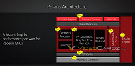
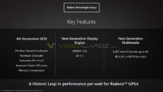
The fourth generation of AMD Graphics CoreNext GPU architecture has been reportedly codenamed "Polaris" by the company. It makes its debut later this year in the company's "Arctic Islands" GPUs, built on Samsung's 14 nm FinFET node. According to the company, Polaris will provide a "historic leap in performance/Watt" for Radeon GPUs. Chips based on Polaris will feature improvements to not just the compute units, but will also come with generational improvements to pretty much every other component, including a new front-end, display controllers, and a new memory controller supporting HBM2.
AMD debuted its first generation GCN architecture with the Radeon HD 7000 series, notably the "Tahiti" silicon. Its second-generation, GCN 2.0, (reported in the press as GCN 1.1), debuted with the R9 290 series, notably the "Hawaii" silicon. The third-generation, GCN 3.0 (reported in the press as GCN 1.2), debuted with the R9 285, notably the "Tonga" silicon; making "Polaris" the fourth-generation. GCN 4.0 will form the core micro-architecture of the "Arctic Islands" family of GPUs, which make their debut in mid-2016.
Source:
VideoCardz
AMD debuted its first generation GCN architecture with the Radeon HD 7000 series, notably the "Tahiti" silicon. Its second-generation, GCN 2.0, (reported in the press as GCN 1.1), debuted with the R9 290 series, notably the "Hawaii" silicon. The third-generation, GCN 3.0 (reported in the press as GCN 1.2), debuted with the R9 285, notably the "Tonga" silicon; making "Polaris" the fourth-generation. GCN 4.0 will form the core micro-architecture of the "Arctic Islands" family of GPUs, which make their debut in mid-2016.
24 Comments on 4th Generation Graphics CoreNext Architecture Codenamed "Polaris"
source
I hope it supports D3D12_1. It's pretty sad that Skylake's GPU has the most D3D12_1 support to date. :cry:
Funny how that slide has spelling correction squiggles. :roll:
Graphics Command Processor --updated-> Command Processor
L2 Cache --updated-> L2 Cache
The only significant changes I see:
- It appears to go from 8 memory controllers to 1. The slide could just be leaving out duplicates (seems likely). Obviously it was updated from HBM1 to HBM2.
- I assume the darker red between Global Data Share and L2 Cache is the "Shader Engine." If Mulmedia Accelerators were removed and replaced with this "Multimedia Cores" inside of each "Shader Engine," that's a major change.
- It doesn't give any indication if it only has one "Shader Engine" or many. If there's only one, that could be a monumental change as well (again, probably just omitting duplicates).
- Is Display Engine just a wrapper for Eyefinity and Crossfire support or something else?
It looks more like GCN 1.3 than GCN 2.0. I am intrigued by these "Multimedia Cores" and "Display Engine" though.Edit: Looking closer at this, it doesn't make sense for there to be many Video Coding Engines (VCE), Unified Video Decoders (UVD), nor TrueAudio Digital Sound Processors (DSP). If it was intentionally placed under the Shader Engine, it is something new.
I suspect the "Display Engine" will include support for DisplayPort 1.3 but it remains to be seen of AMD will bother with HDMI 2.0.
It looks like they rushed the slide to remove the four extra ACEs and add in the two HWS.
Polaris definitely looks like GCN 1.3 to me.
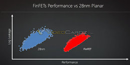
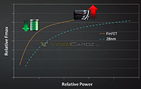
AMD is claiming that the performance per watt is going to be a historic leap. A claim that is hard to dispute, given that the new process will offer dang near 4x the components in the same surface area. This is AMD claiming that their fab finally upgrading after 3 generations is a good thing.
As far as the rest of the claims, aren't they largely focused on software? The same Crimson software that AMD just released.
Despite the PR stupidity, I'm looking forward to Arctic Islands and Pascal. Both of them should finally give me a reason to upgrade from my 7970. Heck, even that's a low bar.