Monday, April 11th 2016

NVIDIA "Pascal" GP104 Silicon Pictured
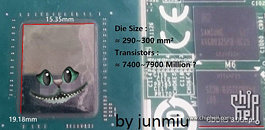
A picture of NVIDIA's next performance-segment GPU based on the upcoming "Pascal" architecture, the GP104, was leaked to the web, revealing a heap of raw material to speculate from. To begin with, GP104 retains the traditional component layout of a simple GPU die sitting on a conventional fiberglass substrate package, with memory chips surrounding it. NVIDIA is reserving exotic specs such as stacked HBM2 memory for the high-end GP100 silicon.
Some fairly straightforward trignometry reveals that the rectangular die of the GP104 measures 15.35 mm x 19.18 mm, with one source speculating a transistor-count of 7.4-7.9 billion. The card is expected to feature 8 gigabit GDDR5 memory chips, which tick at 8 GHz (GDDR5-effective). If the memory bus width is 256-bit, then you're looking at a memory bandwidth of 256 GB/s. The CUDA core count of the GP104 could be closer to 2,560, than the 4,096 from an older report.
Sources:
AnandTech Forums, ChipHell
Some fairly straightforward trignometry reveals that the rectangular die of the GP104 measures 15.35 mm x 19.18 mm, with one source speculating a transistor-count of 7.4-7.9 billion. The card is expected to feature 8 gigabit GDDR5 memory chips, which tick at 8 GHz (GDDR5-effective). If the memory bus width is 256-bit, then you're looking at a memory bandwidth of 256 GB/s. The CUDA core count of the GP104 could be closer to 2,560, than the 4,096 from an older report.

6 Comments on NVIDIA "Pascal" GP104 Silicon Pictured
+30%. That's all folks.