Thursday, May 12th 2016

Micron GDDR5X Memory Chip Pictured Up Close

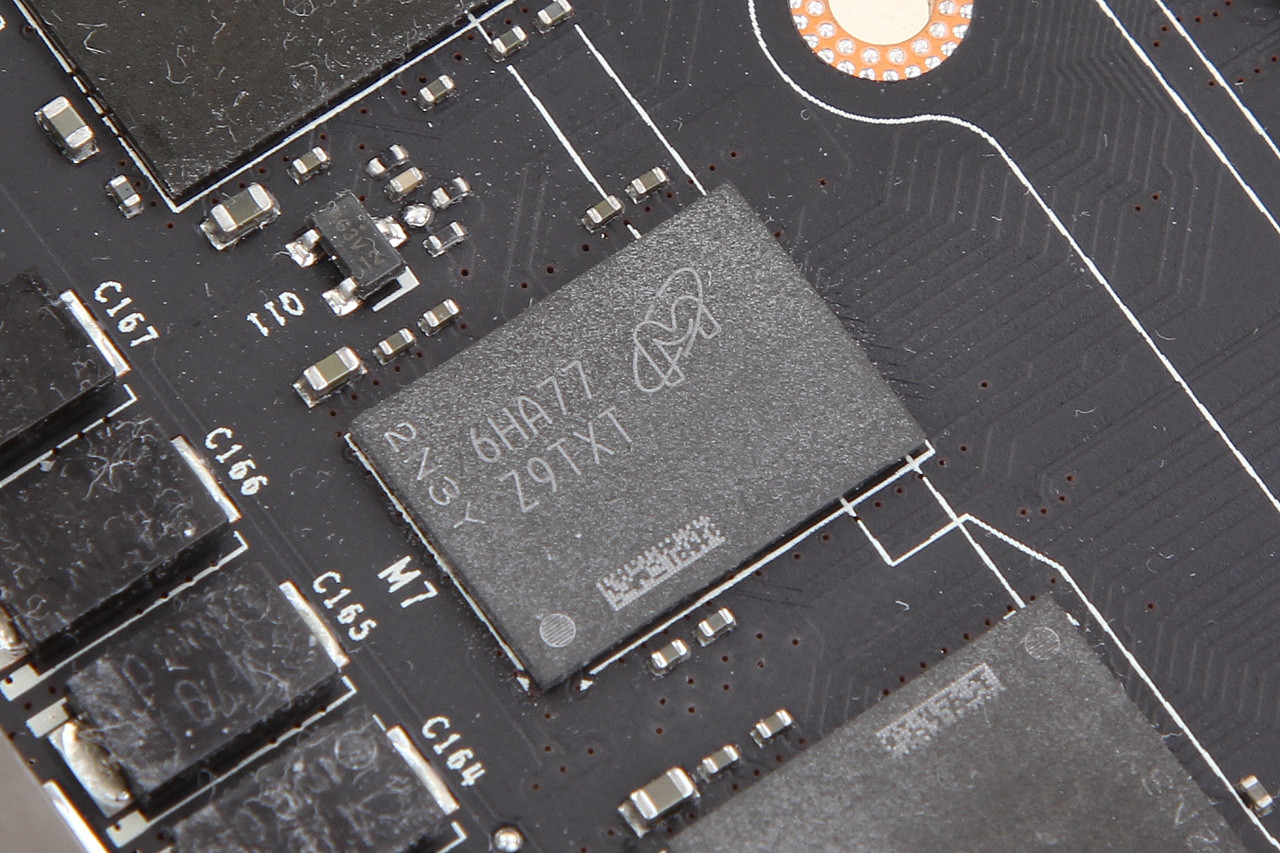
Here are some of the first pictures of a Micron-made GDDR5X memory chip, up close. The picture reveals the 8-gigabit chip's package number "6HA77Z9TXT-2N3Y." The company's part number is "MT58K256M32." The GeForce GTX 1080 is the first production graphics card with GDDR5X memory, and Micron is the first to market with these chips. The GTX 1080 uses eight such 8-gigabit chips across its 256-bit wide memory interface, to make up its 8 GB standard memory amount. The reference-design GTX 1080 features a memory clock speed of 2.50 GHz (actual), or 10 Gbps (effective). The memory bandwidth for the GTX 1080 is a staggering 320 GB/s.

In its company blog post, Micron states: "Designed by our specialized team of Graphics memory engineers in Munich, GDDR5X provides NVIDIA with an unprecedented level of memory bandwidth for their new GeForce GTX 1080. The bandwidth delivered by Micron's GDDR5X memory is the result of thousands of hours of teamwork by some of the most brilliant minds in our two companies." Not only is GDDR5X faster, but also more energy-efficient than the 7 Gbps GDDR5 chips from the previous generation. This particular chip has a module voltage (VDDQ) of 1.35V, its package measures 14 mm x 10 mm x 1.1 mm (LxWxH).
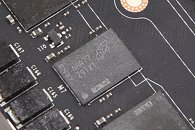
Source: VideoCardz
Add your own comment

31 Comments on Micron GDDR5X Memory Chip Pictured Up Close

#1
beholderidis
I'm so annoyed by such claims when Nvidia thinks it's customers are idiots.

So the latest and greatest Nvidia card with the latest and greatest type of GDDR memory has the exact same bandwidth that with the last 3+ generation of cards.

So let's talk numbers: the bandwidth (B/W) of GTX 1080 is 320 GB/sec, while 980 Ti had 336 GB/sec with only 7GHz memory but 384-bit bus. Then 780 Ti also had 336 GB/sec with the same specs as 980 Ti.

When Micron announced GDDR5X last year they said the frequency will be up to 14GHz, but instead they give us this low performance product of 10GHz (most likely due to low yields, meaning they couldn't produce enough high frequency chips)

So let's assume you are the product manager for this product, the new GPU from Nvidia, and you know you can make a better product even using the 10GHz memory (unfortunately the 11 or 12GHz chips, are just now getting sampled as I read yesterday). but in order to do so you should use a 384-bit bus.
But no, you opt to milk the market for a longer period of time and give out the same performance-wise product, instead of going for 384-bit at 10GHz = 480 GB/sec (almost the same a HBM1 that goes for 512GB/sec).

This memory has a potential of up to 512-bit at 14GHz = ~900 GB/sec. Of course Nvidia would never go for a 512-bit bus so even at 384-bits you could have 670GB/sec B/W on the memory, which is essentially 2 times faster than last year's 336GB/sec.

So let's wait and see how many years will it take to give us this kind of product. I assume by then, HBM2 might be much cheaper so the whole thing might not worth it after all.
Posted on Reply
#2
-The_Mask-
10Gb/s GDDR5x has a frequency of 1,25GHz, that's why it's more energy efficient.
Posted on Reply
#3
happita
HBM2 cards most likely won't arrive until the end of this year (best-case scenario) and when they do, believe me GDDR5X will still be the more viable option for sub-enthusiast cards no matter how you cut it. There are only a few advantages that it has over GDDR5X, but unfortunately they aren't worth the premium memory makers want for it. It'll be a while before HBM2 prices come down, so don't hold your breath. In the meantime, GDDR5X is a welcomed sidegrade from GDDR5.
Posted on Reply
#4
Slizzo
beholderidisI'm so annoyed by such claims when Nvidia thinks it's customers are idiots.

So the latest and greatest Nvidia card with the latest and greatest type of GDDR memory has the exact same bandwidth that with the last 3+ generation of cards.

So let's talk numbers: the bandwidth (B/W) of GTX 1080 is 320 GB/sec, while 980 Ti had 336 GB/sec with only 7GHz memory but 384-bit bus. Then 780 Ti also had 336 GB/sec with the same specs as 980 Ti.

When Micron announced GDDR5X last year they said the frequency will be up to 14GHz, but instead they give us this low performance product of 10GHz (most likely due to low yields, meaning they couldn't produce enough high frequency chips)

So let's assume you are the product manager for this product, the new GPU from Nvidia, and you know you can make a better product even using the 10GHz memory (unfortunately the 11 or 12GHz chips, are just now getting sampled as I read yesterday). but in order to do so you should use a 384-bit bus.
But no, you opt to milk the market for a longer period of time and give out the same performance-wise product, instead of going for 384-bit at 10GHz = 480 GB/sec (almost the same a HBM1 that goes for 512GB/sec).

This memory has a potential of up to 512-bit at 14GHz = ~900 GB/sec. Of course Nvidia would never go for a 512-bit bus so even at 384-bits you could have 670GB/sec B/W on the memory, which is essentially 2 times faster than last year's 336GB/sec.

So let's wait and see how many years will it take to give us this kind of product. I assume by then, HBM2 might be much cheaper so the whole thing might not worth it after all.
I'm failing to see how giving users better memory speed on a card that is in a lower segment than the previous cards you mentioned a bad thing? Remember the GTX1080 is replacing the GTX980, NOT the GTX 980Ti. You could have gotten up in arms if the big Pascal chip were 384bit bus on GDDR5, but with it being on HBM2, your whole point is invalid.
Posted on Reply
#5
ZoneDymo
SlizzoI'm failing to see how giving users better memory speed on a card that is in a lower segment than the previous cards you mentioned a bad thing? Remember the GTX1080 is replacing the GTX980, NOT the GTX 980Ti. You could have gotten up in arms if the big Pascal chip were 384bit bus on GDDR5, but with it being on HBM2, your whole point is invalid.
Eh I dont agree, to me it seems like they are deliberately and cheaply making a product worse then it easily could be so they can milk it for a few more "generations".
Selling 2 cards after eachother for 600 dollars is better then selling 1 card.

And we know, its business, they are out to make money, but again, that does not help us and we should not support it as far as I am concerned.
Posted on Reply
#6
MxPhenom 216
ASIC Engineer
ZoneDymoEh I dont agree, to me it seems like they are deliberately and cheaply making a product worse then it easily could be so they can milk it for a few more "generations".
Selling 2 cards after eachother for 600 dollars is better then selling 1 card.

And we know, its business, they are out to make money, but again, that does not help us and we should not support it as far as I am concerned.
You clearly havent been keeping with with Nvidias last 2 generations of GPUs (kepler and maxwell) Gk104 and Gm104 are mid range dies which are used in the 670/680/970/980, then when big die chips come (GK100 and GM100) they are used in the 780/780Ti/980Ti. Nvidia is doing nothing differently about Pascal.
Posted on Reply
#7
ZoneDymo
MxPhenom 216You clearly havent been keeping with with Nvidias last 2 generations of GPUs (kepler and maxwell) Gk104 and Gm104 are mid range dies which are used in the 670/680/970/980, then when big die chips come (GK100 and GM100) they are used in the 780/780Ti/980Ti. Nvidia is doing nothing differently about Pascal.
ermm nobody is talking about the die chips, we are talking about bus size and gddr5x potential.
Posted on Reply
#8
Slizzo
ZoneDymoermm nobody is talking about the die chips, we are talking about bus size and gddr5x potential.
Right, and he was stating what I stated. GP104 is meant to replace GM204. A 384-bit bus would be expensive and probably not needed for a chip this size, especially since GDDR5x is now on the scene. They can get much more bandwidth out of a smaller bus size.
Posted on Reply
#9
R-T-B
ZoneDymoermm nobody is talking about the die chips, we are talking about bus size and gddr5x potential.
bus size is part of the GPU die.
Posted on Reply
#10
MxPhenom 216
ASIC Engineer
ZoneDymoermm nobody is talking about the die chips, we are talking about bus size and gddr5x potential.
Understand that a large bus, increases the size of the die quite largely. Also more heat and power consumption. WIth GDDR5x, they can increase bandwidth while maintaining the same bus width. the 1080 is pushing more gb/s at 256 bit than a 780 or any 384 bit bus for that matter, while keeping die size, power consumption, and heat low.
Posted on Reply
#11
AsRock
TPU addict
The memory bandwidth for the GTX 1080 is a staggering 320 GB/s.
HUH, haven't cards been doing at least this for years now.
Posted on Reply
#12
Casecutter
Is it me or is this GDDR5X stuff just here to conveniently quick...
It really only came into the common knowledge base back just like 2-3mo's ago, and already hard spec's and sampling. Now it's fully ramped-up and Nvidia has a product base on it? We know GP104 probably first taped out like October '15, A-1 production was like Feb-March '16. So you're telling me Nvidia took a chance on 5X without making any optimization to their memory controller? Or, yes they got early access.

While I grasp the differences, in this "real" implementation as said above it's not pressing the full potential, it's just convenient. Micron probably only first pitched this (just) to Nvidia many months (+18) back. As AMD was in with Hynix and HBM, Micron figured Nvidia would wring their hands over having first crack, and then like become a monetarily partner on the low-down, keeping all the released info late in coming. Like just now, hearing "oh" Micron is in full production. Not long ago it was like production might happen in Q3. Not this hardly the end of Q2 and Nvidia already has it in their factories and cards built with!

I'd bet AMD/RTG didn't get a head-ups on this till like the end of 2015, and by then it was off the drawing board to implement. I'm not saying this isn't business or truly “off the unethical reservation”, but again Nvidia doesn't like working within open standards. Might have a reason for that whole AMD will get first shot at Hynix HBM2 production, while why Samsung and Nvidia had to make up in the courts.

I think it will turn out that GDDR5X is more a means to keep the “bus” to a less costly 256-Bit PCB, all while keeping the bandwidth in the sweet-spot of more 2K. Probably still enough to hold its own in 4K, given the limits of the just 25% more CUDA parts, and not the 40% the 980Ti retained just to sneak into 4K.
But hey the secret could be in the sauce.
Posted on Reply
#13
rtwjunkie
PC Gaming Enthusiast
AsRockHUH, haven't cards been doing at least this for years now.
No, not really. At the place in the Pascal ladder the 1080 sits with its gp104 chip, it is a huge leap forward in bandwidth. My GTX 980, which is directly replaced by 1080, the stock badwidth is 224.4 GB/s. The 320 of the 1080 is a huge increase. It nearly matches the 980Ti 384-bit wide bandwidth.

@Casecutter actually, I recall hearing about GDDR5x right after hearing about HBM. So both manufacturers have known of it for quite awhile. That means Micron started work on this at least a couple years ago.
Posted on Reply
#14
AsRock
TPU addict


I guess it would be much more on a AMD card with a 512bit bus.
Posted on Reply
#15
rtwjunkie
PC Gaming Enthusiast
AsRock


I guess it would be much more on a AMD card with a 512bit bus.
Definately! :-)
Posted on Reply
#16
jabbadap
AsRock


I guess it would be much more on a AMD card with a 512bit bus.
Yep twice as much, 512bit*10Gbps/8=640 GB/s
Posted on Reply
#17
Kanan
Tech Enthusiast & Gamer
#1:
The card has delta compression, it doesn't need more than 320 GB/s. Also this 320 GB/s with delta compression is worth a lot more than 780 Ti's 336 GB/s with 1750 MHz GDDR5 without compression.
The bandwidth of 980 Ti and 1080 are way higher than that of 780 Ti. 780 Ti bandwidth is comparable with that of GTX 980 (224 GB + compression speed up, nearly matching it or more).
So there's no "conspiracy" here. ;)

GDDR5X is a very welcome alternative, HBM2 would make the cards even more expensive. I wonder if GP100 could be made with GDDR5X, I think yes. High clocked (14 GHz) GDDR5X with 384 bit bus, should have easily enough bandwidth compared to HBM2. But it would suck more power I guess.

The only disadvantage of GDDR5X compared to HBM2 on the long run is again the power consumption, nothing really changed compared to GDDR5, it's just a bit better.
Posted on Reply
#18
MxPhenom 216
ASIC Engineer
AsRockHUH, haven't cards been doing at least this for years now.
780ti and 980ti are the only ones unless memory is overclocked on a 780. My 780 will push 320gb/s if memory is at 6.8ghz effective. Mind you those cards have 384 bit buses not 256.

But AMD cards do with 512 bit bus.
Posted on Reply
#19
HumanSmoke
CasecutterIs it me or is this GDDR5X stuff just here to conveniently quick...
It really only came into the common knowledge base back just like 2-3mo's ago,
Your Alzheimer's kicking it up a notch? There was an extensive thread here at TPU almost seven months ago...and you want to know the fun part? YOU provided three of the posts.
Casecutterand already hard spec's and sampling. Now it's fully ramped-up and Nvidia has a product base on it? We know GP104 probably first taped out like October '15, A-1 production was like Feb-March '16. So you're telling me Nvidia took a chance on 5X without making any optimization to their memory controller? Or, yes they got early access.
Obviously the testing and QA undertaken on GDDR5X goes back to around the September 2015 announcement. As many, including Micron themselves, noted, the memory controllers did not need significant redesign.
Since Micron wrote the specification, JEDEC ratification was basically just a rubber stamp job. AFAIK, Micron began a pilot manufacturing line for GDDR5X even before the January ratification happened.
CasecutterI'd bet AMD/RTG didn't get a head-ups on this till like the end of 2015
Because people at AMD have reading and learning disabilities? or because they can't afford an internet connection? :roll: You're telling me, the entire industry and people who might only browse mainstream tech sites are more informed than AMD? Now that would explain a few things.
Casecutterand by then it was off the drawing board to implement. I'm not saying this isn't business or truly “off the unethical reservation”, but...
That's exactly what you appear to be saying. You think this situation is more of a monopoly situation than AMD and Hynix working on HBM out of the public eye at least four years before the first product arrived? :rolleyes::rolleyes::rolleyes::rolleyes:
Keeping stuff secret for years is not worthy of mention, but Micron announcing GDDR5X on 1 September of 2015 and including their immediate intention to make it an open standard (which occurred 4 moths later) is somehow shady?
Posted on Reply
#20
RealNeil
HumanSmokeand you want to know the fun part? YOU provided three of the posts.
LOL!

I keep everything stored in my memory-blank too!
Posted on Reply
#21
TheinsanegamerN
AsRockHUH, haven't cards been doing at least this for years now.
the 980ti has 336GB/s, but that is a much higher bracket. the 1080 replaces the 980, which had 224GB/s. The 780ti could hit it with a memory OC, but maxwell and pascal need less bandwidth for the same performance due to compression. pascal most likely is even more memory efficient then maxwell was.

I find it amazing how many people go rabid over this. "BAH, NVIDIAS NOW HIGH END CARD IS FASTER THAN THE ENTHUSIAST CARD, THEY ARE RIPPING US OFF BECAUSE IT ISNT TWICE AS FAST AS A TITAN X AND DOESNT HAVE A 9000 BIT BUS!!!!1!!1!!1" Every generation is like this, what once took enthusiast class hardware now only takes mid-high to high range hardware, high end is now mid range, ece. The way I see it, the 1080 is twice as fast as the card it replaces, the 980, and is faster than the titan x, while being a much smaller and more energy efficient chip. at 180 watt, it plows the 980 out of the water, and rightly so.
Posted on Reply
#22
Casecutter
HumanSmokeYOU provided three of the posts
Ok, good find I must have not rolled be to the 3rd page of Google returns. I'm glad your the steel trap on everything, and I don't make this full-time venture, more a side thing.
HumanSmokeBecause people at AMD have reading and learning disabilities?
You say originally announced in September 2015, while end of October btarunr posts that a "leaked presentation" all that would've still kept it out of Polaris that was shown early January.
HumanSmokeis somehow shady?
I think the word I used is "convenient" - agreeable to ease in use; favorable, easy, or comfortable for use.
Posted on Reply
#23
HumanSmoke
CasecutterYou say originally announced in September 2015, while end of October btarunr posts that a "leaked presentation" all that would've still kept it out of Polaris that was shown early January.
Yeah, it was so leaked that Micron included GDDR5X in both their Q3 earnings call and even in their September 2015 PR blogs...AND the story was picked up byother tech sites. You are now telling me that AMD ONLY follow TPU as the source of their industry news? If that's the case you'd think they would have nicer to the site and not screwed them over for a Nano review sample.:shadedshu:
Interesting that you completely ignore the fact that AMD and Hynix worked on HBM in secret for years, but that's OK in your book. Hyprocrite. Hypocrite.

I'd continue to debate the point, but you'll just forget this thread ever took place in a few days..........don't worry though, your highly amusing post won't fade into obscurity - I'll see to it.;)


EDIT for grammatical error since Casecutter sees this as having major importance.
Posted on Reply
#24
Casecutter
HumanSmokeAMD and Hynix worked on HBM in secret for years, but that's OK in your book. Hyprocrite.
It's spelt Hypocrite ... Neanderthal. And no Hybrid Memory Cube has been know even before Fuji for like 4 years.
Posted on Reply
#25
HumanSmoke
CasecutterIt's spelt Hypocrite ... Neanderthal. And no Hybrid Memory Cube has been know even before Fuji for like 4 years.
Wooooo typo! Feeling strong now? So what's Fuji?
HMC was designed almost exclusively for Xeon Phi. When Nvidia evinced interest, Intel crushed its development and developed MCDRAM.
Nvidia wasn't working with Intel on HMC. Never had anything to do with HMC (they weren't even a member of the HMC Consortium). Never used HMC. Only ever showed a mock up of what an HMC equipped module would look like. NOT the same thing as actively working on a technology for years. The fact that you are still defending AMD despite this - and almost certainly not knowing anything about HMC (or much else it would seem), makes your posting just look like knee-jerk rants interspersed with AMD shilling.:rolleyes:
Posted on Reply
Add your own comment
Sep 26th, 2024 18:52 EDT change timezone

New Forum Posts

Popular Reviews

Controversial News Posts