Monday, October 5th 2020

AMD "Big Navi" GPU Die Pictured? Allegedly Measures 536mm²

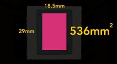
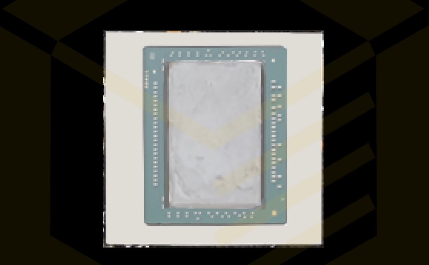
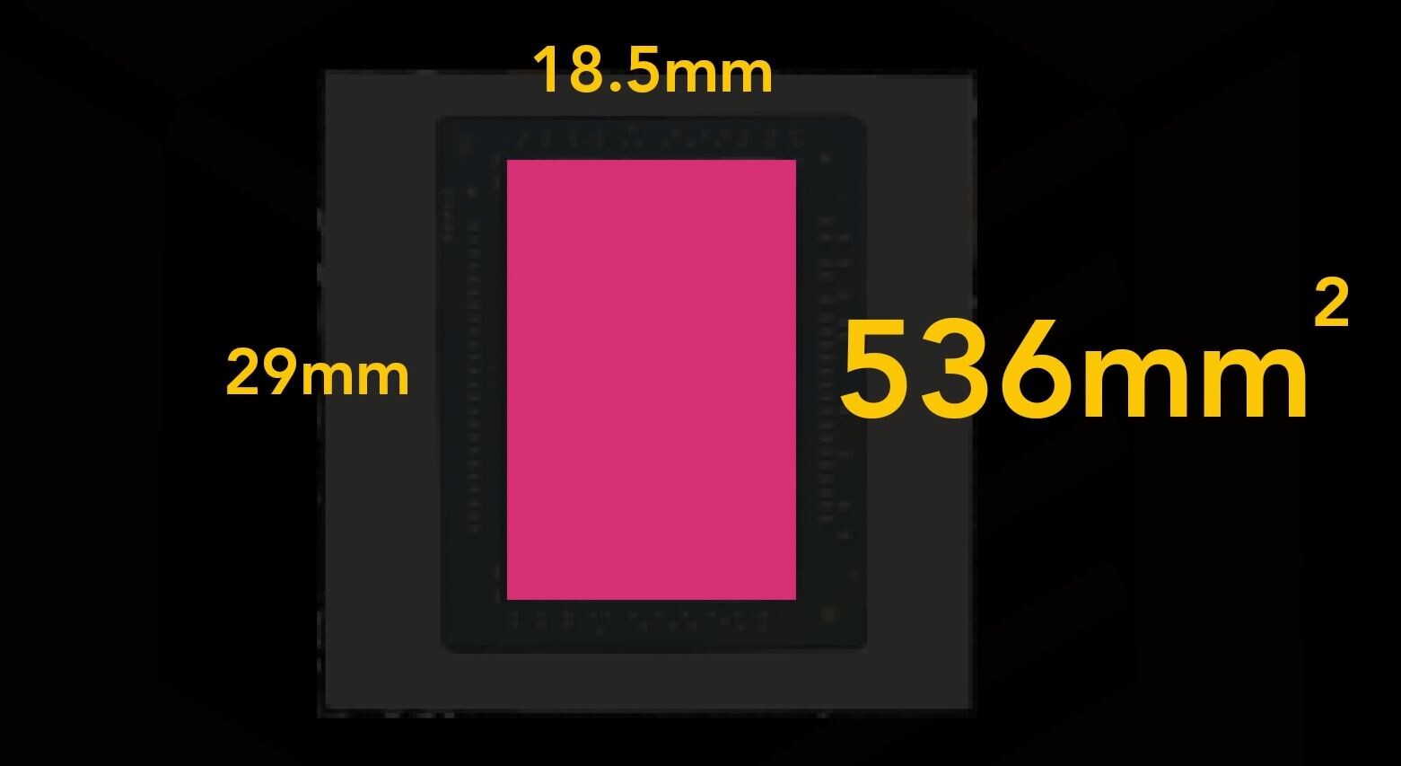
Coreteks, in a video presentation on Sunday, released what is possibly the very first picture of the AMD "Big Navi" GPU silicon, which could power the company's next-generation Radeon RX 6000 series flagship graphics card. The grainy, blurry-cam picture reveals a mostly square package with a large, rectangular die at its center, which Coreteks estimates to be 536 mm² in die-area, with 29 mm x 18.5 mm (LxW) dimensions. The channel used an unusual method for measuring the die size. The chip is rumored to feature around 80 compute units based on the RDNA2 graphics architecture, which includes fixed-function hardware for real-time raytracing, as RDNA2 is designed to meet DirectX 12 Ultimate logo requirements. We'll know more about the chip in the run up to its October 28 unveiling.
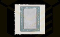
Source: Coreteks (YouTube)
Add your own comment

37 Comments on AMD "Big Navi" GPU Die Pictured? Allegedly Measures 536mm²

#1
ratirt
Yeah. Seen that one yesterday. It may not be necessarily accurate but if this chip is 563mm2 containing 80CUs, that's impressive.
Posted on Reply
#2
Vya Domus
For a chip this big it has to contain more than 80CUs for redundancy. The size is also indicative of those rumored large caches, remember that GPUs don't scale linearly in size, for this chip to be 2.1X in size that must mean that it contains way more than just twice the shaders.
Posted on Reply
#3
ratirt
Vya DomusFor a chip this big it has to contain more than 80CUs for redundancy. The size is also indicative of those rumored large caches, remember that GPUs don't scale linearly in size, for this chip to be 2.1X in size that must mean that it contains way more than just twice the shaders.
I thought that is obvious. RT whatever cores AMD is putting there and the cash is gonna be there as well. Either way, if this is supposed to compete with the 3080 or even 3090, with the size 536mm2 mentioned, it is impressive. 3080 die alone is way bigger than that. Besides this is just speculation and we don't even know if the 536mm2 is correct.
Posted on Reply
#4
Vya Domus
ratirt3080 die alone is way bigger than that.
But a good chunk of it is disabled, the 3080 is missing some 20% of shaders the full die has.
Posted on Reply
#5
laszlo
if we consider die size and transistor density for 7nm tsmc than we look at min.50 billion .... more than in rtx3090 -28 billion...

if is 7nm+ (+?) than even higher count...
Posted on Reply
#6
ratirt
Vya DomusBut a good chunk of it is disabled, the 3080 is missing some 20% of shaders the full die has.
You are right. Anyway, if this one can compete with the 3090 (rumored it can) then it doesn't matter much though. Considering another rumor (2.2 - 2.5 Ghz core for AMD) it doesn't have to have that much CU's. Still the die is smaller than NV Ampere. Either way we still need to wait for the release.
laszloif we consider die size and transistor density for 7nm tsmc than we look at min.50 billion .... more than in rtx3090 -28 billion...

if is 7nm+ (+?) than even higher count...
Actually in the Video Coreteks did and estimated the extrapolation of the 5700xt to evaluate the transistors in the RDNA2, it is not 50 bullion but 26.3 billion. This is all guesses anyway. RDNA 2 is different than RDNA and these rumors may not be true but they do give some insight to an extent.
The video link
Posted on Reply
#7
Vya Domus
laszloif we consider die size and transistor density for 7nm tsmc than we look at min.50 billion .... more than in rtx3090 -28 billion...

if is 7nm+ (+?) than even higher count...
It depends on what it contains, if the rumors are true and a lot of the die is just the cache, then it's probably way more than just double that of Navi 10 as caches are very dense. A100 also has so many transistors mostly because of it's large cache.
Posted on Reply
#8
Anymal
How big proportion of die would it be for rt?
Posted on Reply
#9
ratirt
AnymalHow big proportion of die would it be for rt?
Nobody knows that at this point. It's just estimations and guesses which may turn to be true or totally off what the truth is.
Posted on Reply
#10
Vya Domus
ratirtNobody knows that at this point. It's just estimations and guesses which may turn to be true or totally off what the truth is.
Actually it is known somewhat. There are no RT cores to speak of, the functionality is integrated in the TMUs, what that means is that it probably doesn't take that much space as some of the logic is shared.
Posted on Reply
#11
ratirt
Vya DomusActually it is known somewhat. There are no RT cores to speak of, the functionality is integrated in the TMUs, what that means is that it probably doesn't take that much space as some of the logic is shared.
That's the point. It's always somewhat. To some extent and it turns out to be not as accurate. There has to be some sort of logic to recognize this as RT to process it right. Fact is not a lot is known about the new RDNA2 except some concrete data and loads of rumors. It is true that AMD went with a different approach with the Ray Tracing capabilities.
Posted on Reply
#12
Vya Domus
ratirtThere has to be some sort of logic to recognize this as RT to process it right.
Sure but it must be lower than having a dedicated block, that we know for sure. It's also probably lighter on power as well as you need less connections and data movement between blocks.
Posted on Reply
#14
InVasMani
If AMD is doing RTRT it does stand to reason that there could be some truth to the cache speculations. Really with all the denoise required for RTRT cache could come in real handy.
Vya DomusActually it is known somewhat. There are no RT cores to speak of, the functionality is integrated in the TMUs, what that means is that it probably doesn't take that much space as some of the logic is shared.
That's a interesting tidbit on the TMU's RT cores part. I recall suggesting AMD beef up the TMU's in a discussion awhile back might have been to do with comparing the Vega and RNDA architecture design differences at the time. From what I recall and my memory is foggy on it I think it was something where they could've improved the TMU's by roughly 50% to 100% and had a much improved design where those TMU's actually come into play for scene rendering. Now combine that with the variable rate shading and RTRT and I'm sure that's even more the case. The ROPs count is pretty important as well and obviously compression improvements would made a huge impact for AMD because they are further behind at it.
ratirtYou are right. Anyway, if this one can compete with the 3090 (rumored it can) then it doesn't matter much though. Considering another rumor (2.2 - 2.5 Ghz core for AMD) it doesn't have to have that much CU's. Still the die is smaller than NV Ampere. Either way we still need to wait for the release.
We'll see if the 2.5Hz is possible or not someone was heavily skeptical of AMD achieving a 30%-50% clock speed improvement. One of the things I speculated if that's the case is AMD either not going out of it's way to increase CU's or marginally at best or even using slightly fewer CU's to get higher clock speeds and perhaps they can boost to that speed better, but not really sustain that effectively. We'll just see how stuff pans out I guess time will tell rumors are rumors take them with a grain of salt have has their own speculations of how it could unfold. We'll see what kind of mixed bag it is.

Also this no reasons...just felt it needed to be inserted into the matter. I wonder if anyone's ever been crazy enough to get that as a tattoo.
Posted on Reply
#16
fynxer
Why not put RT cores on separate chip on the graphics card.

Could it be that the coming multi module GPUs will have a separate chip let for the RT cores.
Posted on Reply
#17
Chaitanya
Vya DomusBut a good chunk of it is disabled, the 3080 is missing some 20% of shaders the full die has.
Faulty hence disabled.
Posted on Reply
#18
ratirt
fynxerWhy not put RT cores on separate chip on the graphics card.

Could it be that the coming multi module GPUs will have a separate chip let for the RT cores.
Wouldn't that caused delays and latency issue?
ChaitanyaFaulty hence disabled.
That's not the point and not all of them will be faulty hence the die size of 628 can comprise of the full chip enabled and it will be faster than current top NV card 3090 having more cores.
Posted on Reply
#19
iO
Didn't that guy lose his credibility when he came up with the BS rumour of Ampere having an external RT chip at the back of the card?!
Posted on Reply
#20
Vya Domus
iOHasn't that guy lost his credibility when he came up with the BS rumour of Ampere having an external RT chip at the back of the card?!
I didn't know that someone who speculated on something which turned out to be wrong must lose their credibility. I guess no one on this earth has any credibility in anything.

Anyway, now that I think about it, what were those pictures hiding on the back of the chip ? Well, now we know there were many capacitors there :). Does that mean people knew something was problematic with those from all the way back then ? Food for thought.
Posted on Reply
#21
ratirt
iODidn't lose that guy his credibility when he came up with the BS rumour of Ampere having an external RT chip at the back of the card?!
Credibility about rumors? It's just rumors. How can one lose credibility with that? Things change during the way to full product and credibility about rumors and early news is non existent. It can turn right but it can turn totally different. It's always long way to the final product and things can change.
Just like when AMD changed the BIOS (clocks speeds etc,) for the rx 5000 series few days before release or something like that. How can anyone know that?
Posted on Reply
#22
iO
Vya DomusI didn't know that someone who speculated on something which turned out to be wrong must lose their credibility. I guess no one on this earth has any credibility in anything.

Anyway, now that I think about it, what were those pictures hiding on the back of the chip ? Well, now we know there were many capacitors there :). Does that mean people knew something was problematic with those from all the way back then ? Food for thought.
ratirtCredibility about rumors? It's just rumors. How can one lose credibility with that? Things change during the way to full product and credibility about rumors and early news is non existent. It can turn right but it can turn totally different. It's always long way to the final product and things can change.
Just like when AMD changed the BIOS (clocks speeds etc,) for the rx 5000 series few days before release or something like that. How can anyone know that?
But that 'chip on the back of the card' thing never was a realistic option. You can't just take something as fundamental as the BVH traversal out of the RT rendering pipeline and put it in an extrenal chip without introducing a ton of latency and increased power consumption. Not to mention the problem of cooling a chip on the backside of the PCB.

I guess hiding the back of the chip was meant to prevent people from estamating the die size... And Coreteks saw those pics, counted 1+1=5 and came up with his nonsense theory...
Posted on Reply
#23
Jism
ratirtI thought that is obvious. RT whatever cores AMD is putting there and the cash is gonna be there as well. Either way, if this is supposed to compete with the 3080 or even 3090, with the size 536mm2 mentioned, it is impressive. 3080 die alone is way bigger than that. Besides this is just speculation and we don't even know if the 536mm2 is correct.
5700 was a engineering wonder, pretty much the staff being challenged to make a base chip, medium GPU size and still compete with Nvidia's offerings.

The Big navi is the one really. A tank, large chunks of cache, 80+ CU's, just a overall well optimized arch that will beat the shit out of Nvidia in both power and performance.

Team ATI has bin sleeping for a while, now the bear is woken up.
Posted on Reply
#24
Vya Domus
iOI guess hiding the back of the chip was meant to prevent people from estamating the die size... And Coreteks saw those pics, counted 1+1=5 and came up with his nonsense theory...
You can't estimate the size of a chip from the back of the board. I don't know why you seem to believe that estimating the size of a chip is such a tremendous task, as soon as you have a picture of the chip with components around it the cat is out of the bag.
Posted on Reply
#25
iO
Vya DomusYou can't estimate the size of a chip from the back of the board. I don't know why you seem to believe that estimating the size of a chip is such a tremendous task, as soon as you have a picture of the chip with components around it the cat is out of the bag.
You can get an idea of the die size just from the size of cap array but that's often unreliable and usually more like a wild guess of how big or not the die might be

Posted on Reply
Add your own comment
Jun 3rd, 2024 09:26 EDT change timezone

New Forum Posts

Popular Reviews

Controversial News Posts