Friday, April 5th 2024

AMD Zen 5 Execution Engine Leaked, Features True 512-bit FPU

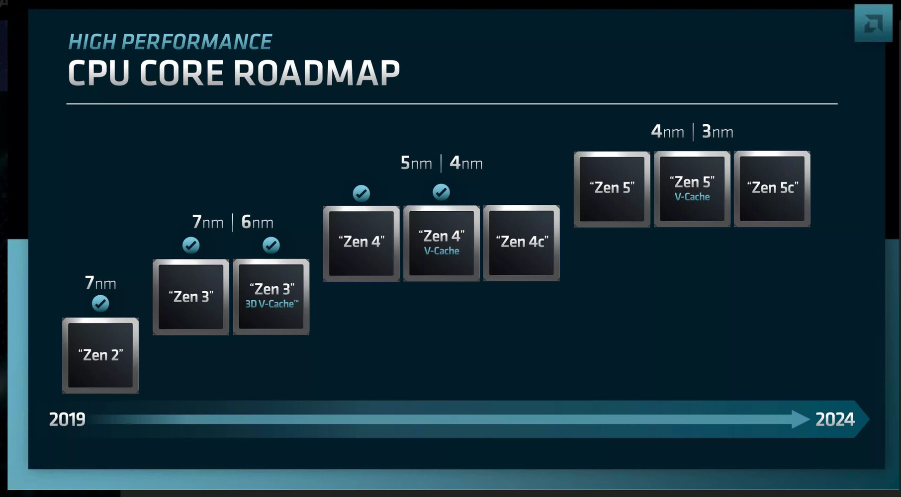
AMD "Zen 5" CPU microarchitecture will introduce a significant performance increase for AVX-512 workloads, with some sources reported as high as 40% performance increases over "Zen 4" in benchmarks that use AVX-512. A Moore's Law is Dead report detailing the execution engine of "Zen 5" holds the answer to how the company managed this—using a true 512-bit FPU. Currently, AMD uses a dual-pumped 256-bit FPU to execute AVX-512 workloads on "Zen 4." The updated FPU should significantly improve the core's performance in workloads that take advantage of 512-bit AVX or VNNI instructions, such as AI.

Giving "Zen 5" a 512-bit FPU meant that AMD also had to scale up the ancillaries—all the components that keep the FPU fed with data and instructions. The company therefore increased the capacity of the L1 DTLB. The load-store queues have been widened to meet the needs of the new FPU. The L1 Data cache has been doubled in bandwidth, and increased in size by 50%. The L1D is now 48 KB in size, up from 32 KB in "Zen 4." FPU MADD latency has been reduced by 1 cycle. Besides the FPU, AMD also increased the number of Integer execution pipes to 10, from 8 on "Zen 4." The exclusive L2 cache per core remains 1 MB in size.
Update 07:02 UTC: Moore's Law is Dead reached out to us and said that the slide previously posted by them, which we had used in an earlier version of this article, is fake, but said that the information contained in that slide is correct, and that they stand by the information.
Source: Moore's Law is Dead (YouTube)
Add your own comment

63 Comments on AMD Zen 5 Execution Engine Leaked, Features True 512-bit FPU

#26
bug
SL2You mean due to smaller die? Yeah, I don't think that's gonna happen.

I mean, of course AMD could lower the price for various reasons, but the reason being smaller die size alone isn't very likely I'm afraid.
Die size makes the biggest impact on the retail price of a CPU. Waffers have predetermined sizes, they cost the same to make. The more chips you turn them into, the lower the price.
Posted on Reply
#27
Philaphlous
I'm sure the shutdown at TSMC from the earthquakes will definitely impact AMD...Delay or reduced shipments if delivered on time...
Posted on Reply
#28
529th
Wonder if this will be a compelling upgrade for Zen3 gamers.
Posted on Reply
#29
windwhirl
DenverI'd just like to see more mainstream consumer applications using such an instruction set.
There are some mainstream uses, such as Blender and some image/video encoding/decoding libraries, but not much else. Maybe RPCS3 if you want to consider PS3 emulation as "mainstream"
529thWonder if this will be a compelling upgrade for Zen3 gamers.
Gotta change board and RAM for this, at least, so it'd probably need some impressive numbers (+20% over Zen4).
Posted on Reply
#30
Redwoodz
PhilaphlousI'm sure the shutdown at TSMC from the earthquakes will definitely impact AMD...Delay or reduced shipments if delivered on time...
I'm sure everyone will be impacted, nothing different about AMD.
Posted on Reply
#31
evernessince
bugIf run locally, maybe. But currently most models worth anything are too big to run a consumer PC. And that's not going to change: no matter how capable PCs will grow, the cloud will always be better.
This is simply not true. You have large models like Llama2, Mistral, ect with a massive amount of parameters working well on regular desktop PCs. You also have Stable diffusion XL and the upcoming stable diffusion 3 models. There's also plenty of AI models that don't require much to run like AI voice enhancers, voice isolation, layer isolation, ect. You are assuming that every AI model worth having is super big and resource intensive but you can see from things like DLSS and SDXL Lighting that AI can be a powerful tool without needing a massive amount of resources. These smaller models can be extremely handy and light on resources.
Posted on Reply
#32
ScaLibBDP
Here a couple of comments...

- A source for that leak is Very Questionable

- Intel AVX-512 ISA is a Complete Tech Disaster ( * )

( * )
It is based on my experience using an Intel Xeon Phi server. We reached its performance limitations in less than 4 weeks after a project was started.
Posted on Reply
#33
ncrs
bugI'm a bit confused. A few years ago we were burning Intel to the stake for AVX-512 (linuxiac.com/linus-torvalds-criticizes-intel-avx-512/, but not only). Now we're cheering for the same AVX-512?
We were burning Intel at the stake because their implementation was subpar. Engaging early AVX-512 implementations caused severe downclocking for the entire CPU even if only a single core was using it. The same issue affected AVX2 to a lesser extent. This made using AVX-512 a hazard for normal CPU operations, often resulting in performance significantly worse than AVX/AVX2 versions.
Since then Intel designs have reduced the penalty and almost eliminated it altogether for Sapphire Rapids.
bugThermal have certainly improved, but the discussion was more about the large amount of die space being used for specialized purposes. That's still the case. Considering the increased competition for fab capacity, you'd think "wasted" transistors is more of o problem today than it was 4 years ago.
Even with an older Skylake-X implementation that contained 2 AVX-512-capable units (one created by combining two 256-bit units, and one dedicated) the difference isn't as big, since only the red part is "dedicated" for AVX-512. Obviously there's other parts of the CPU that need to be extended for it as well.


Source
bugI'm a bit more in the other camp: if it only benefits like 10% of the typical workloads, I'd rather do without and have CPUs that are 20-30% cheaper instead.

At the same time, I realize this is basically a chicken-and-egg problem: if AVX-512 isn't available, apps that use it won't be either.
Current Intel desktop/mobile P-cores contain the transistors for one AVX-512 unit (the combined 2x256-bit), and the miscellaneous stuff all over the core. The server parts extend this base core with a second dedicated 512-bit unit, more cache, a mesh agent and an AMX unit, among other things we can't be sure of just from die shots.
Meteor Lake is also built on the same principle using Redwood Cove cores. It would be prohibitively expensive for Intel to design a special version of the core without them when the combined unit is used for AVX2 anyway. All that makes the E-core business even more controversial.
I doubt purging AVX-512 completely would result in 20-30% less area.

Gains from AVX-512 can be significant, some benchmarks on Phoronix show up to 20x improvement using AVX-512-FP16, but most are not as drastic. Another recent gain of 10x in AI LLM prompt evaluation speed. We're starting to see some Linux distributions compiling software specifically for the x86-64-v4 target which includes AVX-512. It's not only about the vector length, since AVX-512 contains other general improvements usable even by strictly integer-based software.
Posted on Reply
#34
JohH
In znver5 FP store ports are fused for 512-bit operations but can be used separately for 256-bit operations. In some AVX(2) workloads this will improve performance as well.

(define_reservation "znver5-fp-store256" "znver5-fp-store0|znver5-fp-store1")
(define_reservation "znver5-fp-store-512" "znver5-fp-store0+znver5-fp-store1")
Posted on Reply
#35
Daven
bugDie size makes the biggest impact on the retail price of a CPU. Waffers have predetermined sizes, they cost the same to make. The more chips you turn them into, the lower the price.
Don’t forget the law of mass production where reductions in cost can be achieved at scale. It’s cheaper to make millions of a single complex, large core design than a much smaller volume of a few simpler, smaller cores. That’s why AMD has the same chiplet for both Epyc and Ryzen.
Posted on Reply
#37
Denver
RedwoodzI'm sure everyone will be impacted, nothing different about AMD.
It shouldn't, the fab that produces 5nm chips was not impacted. TSMC also left its financial guidance unchanged
Posted on Reply
#38
529th
windwhirlGotta change board and RAM for this, at least, so it'd probably need some impressive numbers (+20% over Zen4).
Atleast %20 at the bottom performing increases!
Posted on Reply
#39
bug
R-T-BThe criticism was due to the product segmentation not the product.
You didn't even open the link I provided, did you?
Posted on Reply
#40
Panther_Seraphin
bugYou didn't even open the link I provided, did you?
Read what he says

He complains at the time that Intel were trying to market AVX512 as the magic bullet to solve all problems. When in actual fact if you used it, it was horrible.

You run AVX512 code on Alder lake and your down in 3.5Ghz Territory when the Turbos were 5Ghz+ for most other things. It also meant the P Cores were physically larger per core for near 0 benefit for most work loads where as a 10-12 core design with only AVX2 would have been better for most use cases. And the other half of your die was completely useless for doing AVX512 workload so there was also that as you had to disable your E cores to use it effectively.


AMD at the time were giving him everything he wanted. More cores, Decent power levels/consumption per core and no gimmicky tools to use to extract extra performance. As he stated at the time AVX512 should have been only in HPC/Server areas and the desktop had little to no benefit from it then.
Posted on Reply
#41
R-T-B
bugYou didn't even open the link I provided, did you?
I've read it before. I know what Torvalds argues.

Have a quote:
He also cautioned against placing too much weight on floating-point performance benchmarks. Especially those that take advantage of exotic new instruction sets that have a fragmented and varied implementation across product lines.
Posted on Reply
#42
user556
Oh, man, what a huge let-down. I had my hopes up it was the general instruction pipeline that was up by 40%. But alas not it seems.

Zen4 AVX512 is already a huge winner the way it is. It single-handedly turned the AVX512 ship around. It didn't need any measurable extra power to do amazing amounts of work. I now fear Zen5 is not going to be that good.
Posted on Reply
#43
JohH
user556Oh, man, what a huge let-down. I had my hopes up it was the general instruction pipeline that was up by 40%. But alas not it seems.

Zen4 AVX512 is already a huge winner the way it is. It single-handedly turned the AVX512 ship around. It didn't need any measurable extra power to do amazing amounts of work. I now fear Zen5 is not going to be that good.
Because of a fake slide?
The way Zen 5 implements 512-bit operations is not yet clear. It may simply be fusing ports fp0/fp1, like they do for stores, in one cycle instead of doing it sequentially. It wouldn't take much extra area. Nor extra power compared to a dense AVX2 loop.

And what we do have evidence for from Zen 5 changes to Linux and GCC suggests general pipeline improvements too. 8 wide dispatch from micro-op cache, 6 ALU and 4 AGU. The only confirmed change for FP is a second FP store unit which does suggest improved throughput of AVX2 and AVX512 programs.

And where did you get the idea it'd be 40% faster? Discredited RDNA3 hypebeasts on twitter?
Posted on Reply
#44
Onasi
JohHAnd where did you get the idea it'd be 40% faster? Discredited RDNA3 hypebeasts on twitter?
Yeah, this should obviously be ridiculous - there hasn’t been a gen on gen improvement this massive… in a while. Not solely from the general instructions. Definitely not between generations of the same architecture. Otherwise we would be talking about a jump in overall performance that would be the biggest for AMD since Zen 1 when compared to Bulldozer and its derivatives. CPUs simply don’t increase in performance this drastically. Even the leaks and estimates for Zen 5 go for saner numbers like 10-15% IPC improvement (plausible) and 20-30% overall performance uplift compared to Zen 4 (again, tracks pretty well with what we’ve seen with previous gen increases, Zen+ aside for obvious reasons).
Posted on Reply
#45
efikkan
stimpy88The low L2 cache size is an obvious planned mistake and low hanging fruit for Zen 6 to fix, we know AMD were experimenting with larger L2 cache sizes, and that 2MB was the sweet spot, and 3MB offering only slight low single-digit uplift in perf over 2MB. One of the reasons for the infamous "AMD dip".
Even though we know the slide is fake, I just want to point out that no one, including the best engineers, could precisely assess the effect of a cache change without evaluating the performance of a specific microarchitecture. A change in cache size on one microarchitecture might not translate to the same proportional change on another. L2 and L1 especially, is very tied to how the pipeline works, which is why the cache configuration might change a lot between generations. And contrary to what most people believe, they don't design the microarchitecture around the cache, it's the other way around. If throwing in another MB or so would make a huge benefit, I'm sure they would. They do simulate all kinds of core configurations before they do a tapeout, so they have quite likely already simulated what a larger L2 cache, and whichever they pick is the overall best performing within the constraints of the architecture and node.

Also, keep in mind there are many more attributes than just size, like latency, number of banks, bandwidth, etc. If the next generation is moved to a new node with different characteristics, it may be achievable with e.g. a larger cache without worsening the latency significantly.
Additionally, many heavy AVX workloads are more sensitive to bandwidth than cache size.
stimpy88And it's also borderline criminal AMD do not rectify the L3 cache starvation issue without the "3D cache band-aid" cash grab. Even a better memory controller would help in this regard.
I've often criticized the large L3, as it's a very "brute force" attempt to make up for shortcomings in the architecture, a sort of "band-aid" like you rightfully call it. But if Zen 5 is significantly better, especially in the front-end and scheduling of instructions, the usefulness of extra L3 may be actually reduced.
There will obviously still be the edge-case scenarios where the extra L3 shines (mostly very bloated code), but the overall gain is close to negligible, and it's such a waste of silicon for most uses.
WirkoAVX512 is for integer and bitwise operations too, not only for FP. That's where SPEC-int gains, purportedly very big, come from.
AVX certainly support integer operations too as you say, but I suspect SPECint isn't compiled to use it, although I haven't checked thoroughly. But even so, modern CPUs do auto-vectorize in some cases, but I don't know if the front-end will be fast enough to vectorize more than 4 64-bit or 8 32-bit ops (per vector unit, so 2x) per clock. I suspect it will be very underutilized in reality, but still, in the worst case with AMD having their vector units on separate execution ports, it will allow each vector unit to work as a single ALU. Or probably split, so each FMA-pair as ALU+MUL. (whether it's worth it in power draw is uncertain)
Posted on Reply
#47
Daven
I for one am glad the nonsense of a one year cadence between Zen 4 and Zen 5 is dead. So many were saying why buy Zen 4 when Zen 5 would come a year later. AMD processor architectures are on a two year cadence just like GPUs. Its possible it could be up to six months early or up to six months late for some releases as circumstances dictate. But never less or more than that for a major release.

Longer cadence with more features and performance on the same established platform as the last gen. This is a big reason I buy AMD.
Posted on Reply
#48
evernessince
user556Oh, man, what a huge let-down. I had my hopes up it was the general instruction pipeline that was up by 40%. But alas not it seems.

Zen4 AVX512 is already a huge winner the way it is. It single-handedly turned the AVX512 ship around. It didn't need any measurable extra power to do amazing amounts of work. I now fear Zen5 is not going to be that good.
I'll assume based on your reaction here that you are not into tech news enough to know that a single slide cannot contain all the details of a given chip. Typically the press is given a deck of slides, not just a single slide, when a company releases a new CPU or GPU.

Nevermind that the slide turned out to be fake, you are drawing a conclusion based on wholly incomplete information. As usual with these kind of rumors and "leaked" slides, they are designed to generate clicks and engagement like what you've provided here. Don't fall for it, wait for official info to draw an informed conclusion.
Posted on Reply
#49
kondamin
SL2You mean due to smaller die? Yeah, I don't think that's gonna happen.

I mean, of course AMD could lower the price for various reasons, but the reason being smaller die size alone isn't very likely I'm afraid.
AMD does chiplets, they can just cut back the number of cores per chiplet and have small dies.
Posted on Reply
#50
phints
Not clear to me why they would put all that die realestate into AVX-512 when almost no one uses them outside game emulators, unelss there is some added push for AI workloads there that I don't know about since everyone is advertising that now.

Silly leaks aside this should finally be a very exciting year for HEDT CPUs.
Posted on Reply
Add your own comment
May 21st, 2024 01:54 EDT change timezone

New Forum Posts

Popular Reviews

Controversial News Posts