Report an Error


AMD Blackcomb
Blackcomb

Shane Phillips
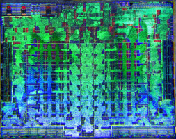
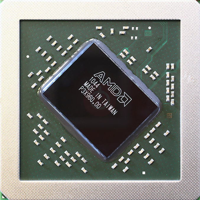
Die Shot
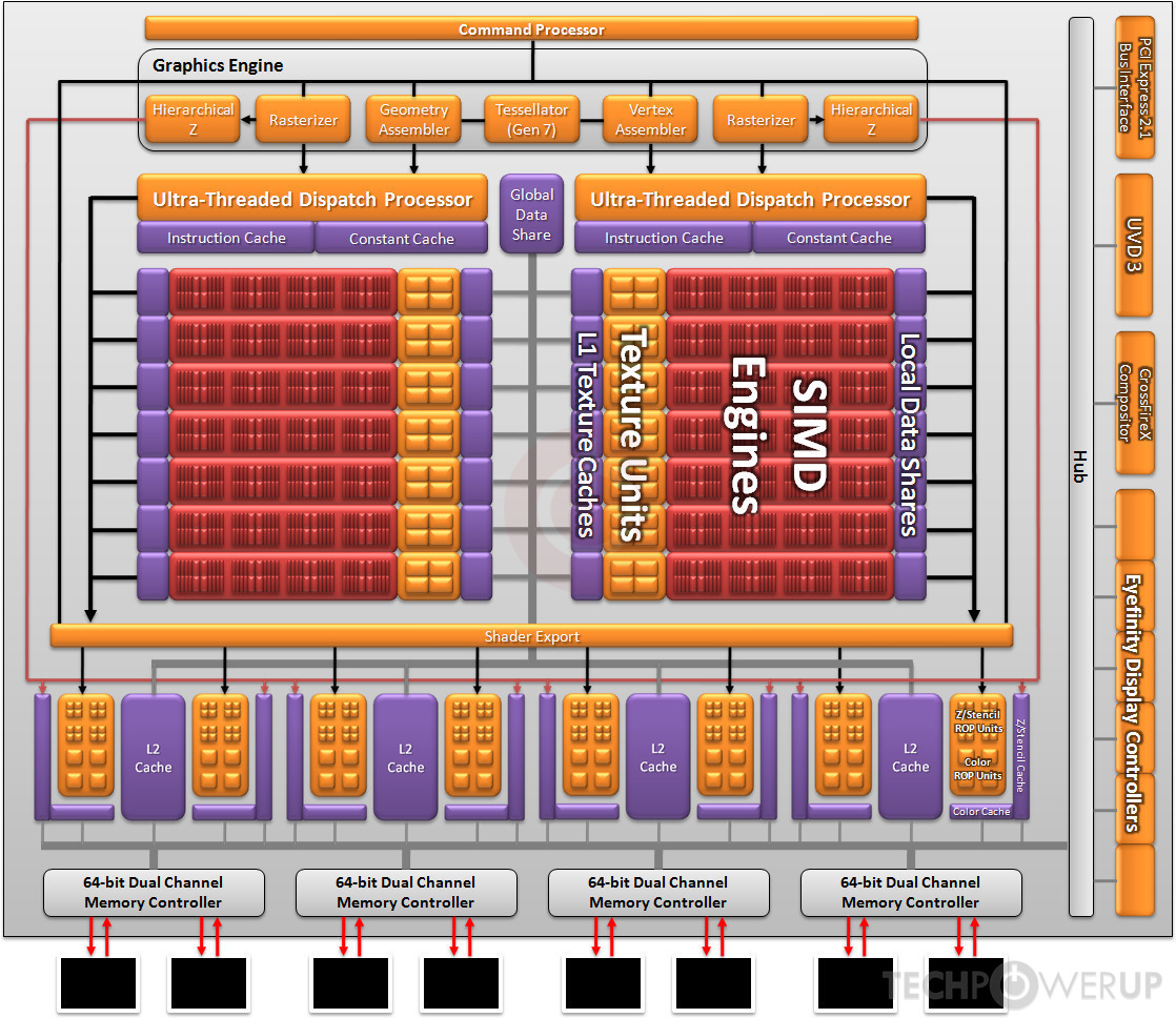
Block Diagram
AMD's Blackcomb GPU uses the TeraScale 2 architecture and is made using a 40 nm production process at TSMC. With a die size of 212 mm² and a transistor count of 1,700 million it is a medium-sized chip. Blackcomb supports DirectX 11.2 (Feature Level 11_0). For GPU compute applications, OpenCL version 1.2 can be used. It features 1120 shading units, 56 texture mapping units and 32 ROPs.
Further reading:
TeraScale 2 Instruction Set Architecture 
Graphics Processor
- Released
- Jan 4th, 2011
- GPU Name
- Blackcomb
- Desktop Variant
- Barts
- Codename
- Victoria
- Generation
- Northern Islands
- Architecture
- TeraScale 2
- Foundry
- TSMC
- Process Size
- 40 nm
- Transistors
- 1,700 million
- Density
- 8.0M / mm²
- Die Size
- 212 mm²
- Package
- HFCBGA-1737
Graphics Features
- DirectX
- 11.2 (11_0)
- OpenGL
- 4.4
- OpenCL
- 1.2
- Vulkan
- N/A
- Shader Model
- 5.0
- WDDM
- 1.3
- Compute
- GFX4
- DCE
- 5.0
- UVD
- 3.1
Render Config
- Shading Units
- 1120
- TMUs
- 56
- ROPs
- 32
- Compute Units
- 14
- Z-Stencil
- 40
- L1 Cache
- 8 KB per CU
- L2 Cache
- 512 KB
- Max. TDP
- 150 W
All TeraScale 2 GPUs
- AMD Barts
- AMD Blackcomb
- ATI Broadway
- AMD Broadway
- AMD Caicos
- AMD Capilano
- ATI Cedar
- AMD Cedar
- ATI Cypress
- AMD Cypress
- AMD Granville
- ATI Hemlock
- AMD Juniper
- ATI Juniper
- AMD Latte
- AMD Lexington
- AMD Loveland
- ATI Madison
- AMD Onega
- ATI Park
- AMD Park
- ATI Pinewood
- AMD Pinewood
- ATI Redwood
- AMD Redwood
- AMD Robson
- AMD Seymour
- AMD Sumo
- AMD SuperSumo
- AMD Thames
- AMD Turks
- ATI Turks
- AMD Whistler
AMD GPU Architecture History
Graphics cards using the AMD Blackcomb GPU
| Name | Chip | Memory | Shaders | TMUs | ROPs | GPU Clock | Memory Clock |
|---|---|---|---|---|---|---|---|
| Blackcomb XTX | 2 GB | 1120 | 56 | 32 | 715 MHz | 900 MHz | |
| Blackcomb XT | 1024 MB | 960 | 48 | 32 | 680 MHz | 900 MHz | |
| Blackcomb PRO | 1024 MB | 960 | 48 | 32 | 580 MHz | 900 MHz | |
| Blackcomb XT GL | 2 GB | 960 | 48 | 32 | 680 MHz | 900 MHz | |
| Blackcomb XT | 2 GB | 960 | 48 | 32 | 680 MHz | 900 MHz | |
| Blackcomb XT | 2 GB | 960 | 48 | 32 | 680 MHz | 900 MHz |


Blackcomb GPU Notes
| Generation: Northern Islands Desktop Variant: Barts Graphics/Compute: GFX4 Display Core Engine: 5.0 Unified Video Decoder: 3.1 |
Jun 10th, 2024 17:46 EDT
change timezone
Latest GPU Drivers
New Forum Posts
- Question about bios flash (7)
- The Filthy, Rotten, Nasty, Helpdesk-Nightmare picture clubhouse (2641)
- my computer hit a wall and cant move data (47)
- Acer Nitro 5 Extreme Overheating - Tried Everything, Don't Know What To Do (2)
- 9900X3D - Will AMD solve the split CCD issue (197)
- Memory Clock reported by GPU-Z and Nvidia performance overlay. (7)
- New Acer Helios 18 i9-14900hx constant throttle @ 94-100c (21)
- How to quickly & easily fix coil-whine(coil choke noise) (874)
- PC doesn't turn on or instantly turns off. (6)
- Sapphire RX580 Nitro+ Thermal Pads (2)
Popular Reviews
- Pulsar Xlite V3 Review
- Intel Lunar Lake Technical Deep Dive - So many Revolutions in One Chip
- Upcoming Hardware Launches 2024 (Updated May 2024)
- NZXT H6 Flow RGB Review
- AQIRYS HYDRA 360 AIO Review
- AMD Ryzen 7 7800X3D Review - The Best Gaming CPU
- Thermal Grizzly KryoSheet Review - Tested on RX 7900 XTX with 475 W
- Ghost of Tsushima Performance Benchmark Review - 35 GPUs Tested
- Kioxia Exceria Plus G3 2 TB Review
- ASUS Radeon RX 7900 GRE TUF OC Review
Controversial News Posts
- AMD RDNA 5 a "Clean Sheet" Graphics Architecture, RDNA 4 Merely Corrects a Bug Over RDNA 3 (144)
- NVIDIA RTX 5090 "Blackwell" Founders Edition to Implement the "RTX 4090 Ti" Cinderblock Design (118)
- AMD Zen 5 Storms into Gaming Desktops with Ryzen 9000 "Granite Ridge" Processors (100)
- Biden Administration to Revive Trump-Era Tariffs on China-made GPUs and Motherboards (95)
- ASRock Innovates First AMD Radeon RX 7000 Graphics Card with 12V-2x6 Power Connector (94)
- AMD Ryzen 9000 Zen 5 Single Thread Performance at 5.80 GHz Found 19% Over Zen 4 (92)
- AMD Ryzen 9000 Zen 5 "Granite Ridge" Desktop Processors Launch Late-July (83)
- AMD to Discontinue Windows 10 Support for its Ryzen 9000 "Strix Point" Mobile Processors (82)