Report an Error


AMD Scarlett

Scarlett

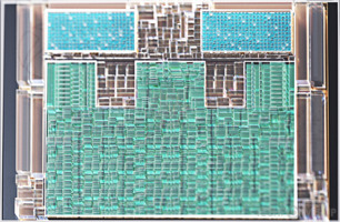
Die Shot

CGI Die Shot

Block Diagram

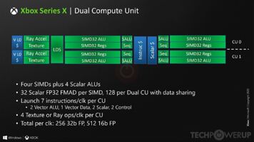
CU Diagram
AMD's Scarlett GPU uses the RDNA 2.0 architecture and is made using a 7 nm production process at TSMC. With a die size of 360 mm² and a transistor count of 15,300 million it is a large chip. Scarlett supports DirectX 12 Ultimate (Feature Level 12_2). For GPU compute applications, OpenCL version 1.2 can be used. Additionally, the DirectX 12 Ultimate capability guarantees support for hardware-raytracing, variable-rate shading and more, in upcoming video games. It features 3584 shading units, 224 texture mapping units and 64 ROPs.
Further reading:
RDNA Whitepaper 
Graphics Processor
- Released
- Nov 10th, 2020
- GPU Name
- Scarlett
- Codename
- Arden
- Generation
- Navi II
- Architecture
- RDNA 2.0
- Foundry
- TSMC
- Process Size
- 7 nm
- Transistors
- 15,300 million
- Density
- 42.5M / mm²
- Die Size
- 360 mm²
- Package
- BGA-2693
- Package Size
- 52.5mm x 52.5mm
Graphics Features
- DirectX
- 12 Ultimate (12_2)
- OpenGL
- 4.6
- OpenCL
- 1.2
- Vulkan
- 1.2
- Shader Model
- 6.7
- WDDM
- 3.1
- GC
- 10.2.0
- Shader ISA
- GFX10.2 (gfx1020)
- DCN
- 3.1
- VCN
- 2.4
Render Config
- Shading Units
- 3584
- TMUs
- 224
- ROPs
- 64
- Compute Units
- 56
- L2 Cache
- 5120 KB
- Max. TDP
- 200 W
All RDNA 2.0 GPUs
AMD GPU Architecture History
- 2023 CDNA 3.0
- 2022-2024 RDNA 3.0
- 2021 CDNA 2.0
- 2020 CDNA 1.0
- 2020-2023 RDNA 2.0
- 2019-2020 RDNA 1.0
- 2018-2022 GCN 5.1
- 2017-2020 GCN 5.0
- 2016-2020 GCN 4.0
- 2014-2019 GCN 3.0
- 2013-2017 GCN 2.0
- 2011-2020 GCN 1.0
- 2010-2013 TeraScale 3
- 2009-2015 TeraScale 2
- 2005-2013 TeraScale
- 2005-2007 Ultra-Threaded SE
Graphics cards using the AMD Scarlett GPU
| Name | Chip | Memory | Shaders | TMUs | ROPs | GPU Clock | Memory Clock |
|---|---|---|---|---|---|---|---|
| 10 GB | 3328 | 208 | 64 | 1825 MHz | 1750 MHz |

Scarlett GPU Notes
| Generation: Navi II Codename: Arden Ray Tracing Cores: 1st Gen Graphics/Compute: 10.2.0 Shader ISA: GFX10.2 (gfx1020) Display Core Next: 3.1 Video Core Next: 2.4 |
May 20th, 2024 16:20 EDT
change timezone
Latest GPU Drivers
New Forum Posts
- My anti budget PC (27)
- Fractal define R4 vs R5 build quality. (15)
- Would you pay more for hardware with AI capabilities? (43)
- EK seems to be having major issues (120)
- What are you playing? (20714)
- For general use - moving files around and playing games, would you have an Optane boot drive or PCie gen 5? (53)
- What's your latest tech purchase? (20593)
- Post Your TIMESPY, PCMARK10 & FIRESTRIKE SCORES! (2019) (223)
- MSI BIOS Undervolting issue (0)
- TPU's Nostalgic Hardware Club (18513)
Popular Reviews
- Ghost of Tsushima Performance Benchmark Review - 35 GPUs Tested
- TerraMaster D8 Hybrid Review
- Silverstone Shark Force 120 mm Fan Review
- Lofree Edge Ultra-Low Profile Wireless Mechanical Keyboard Review
- Homeworld 3 Performance Benchmark Review - 35 GPUs Tested
- Ghost of Tsushima: DLSS vs. FSR vs. XeSS Comparison Review
- Upcoming Hardware Launches 2023 (Updated Feb 2024)
- PNY XLR8 Gaming EPIC-X RGB DDR5-6400 CL32 32 GB Review
- Sapphire Radeon RX 7700 XT Pure Review
- AMD Ryzen 7 7800X3D Review - The Best Gaming CPU
Controversial News Posts
- Intel Statement on Stability Issues: "Motherboard Makers to Blame" (269)
- AMD to Redesign Ray Tracing Hardware on RDNA 4 (227)
- Windows 11 Now Officially Adware as Microsoft Embeds Ads in the Start Menu (173)
- NVIDIA to Only Launch the Flagship GeForce RTX 5090 in 2024, Rest of the Series in 2025 (154)
- AMD Hits Highest-Ever x86 CPU Market Share in Q1 2024 Across Desktop and Server (140)
- AMD RDNA 5 a "Clean Sheet" Graphics Architecture, RDNA 4 Merely Corrects a Bug Over RDNA 3 (139)
- AMD's RDNA 4 GPUs Could Stick with 18 Gbps GDDR6 Memory (114)
- AMD Ryzen 9 7900X3D Now at a Mouth-watering $329 (104)