Report an Error


NVIDIA GeForce GTX 780 Ti Engineering Sample
- Graphics Processor
- GK180
- Cores
- 2880
- TMUs
- 240
- ROPs
- 48
- Memory Size
- 3 GB
- Memory Type
- GDDR5
- Bus Width
- 384 bit

GPU
I/O
Top
Recommended Gaming Resolutions:
- 1920x1080
- 2560x1440
- 3840x2160
The GeForce GTX 780 Ti Engineering Sample was a graphics card by NVIDIA, that was never released. Built on the 28 nm process, and based on the GK180 graphics processor, in its GK180-425-A1 variant, the card supports DirectX 12. Even though it supports DirectX 12, the feature level is only 11_0, which can be problematic with newer DirectX 12 titles. The GK180 graphics processor is a large chip with a die area of 561 mm² and 7,080 million transistors. It features 2880 shading units, 240 texture mapping units, and 48 ROPs. NVIDIA has paired 3,072 MB GDDR5 memory with the GeForce GTX 780 Ti Engineering Sample, which are connected using a 384-bit memory interface. The GPU is operating at a frequency of 875 MHz, which can be boosted up to 928 MHz, memory is running at 1753 MHz (7 Gbps effective).
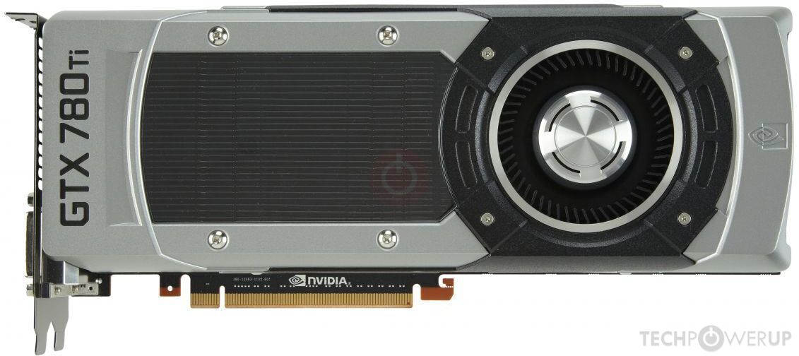
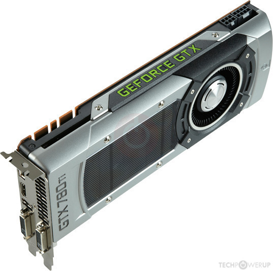
Being a dual-slot card, the NVIDIA GeForce GTX 780 Ti Engineering Sample draws power from 1x 6-pin + 1x 8-pin power connector, with power draw rated at 250 W maximum. Display outputs include: 2x DVI, 1x HDMI 1.4a, 1x DisplayPort 1.2. GeForce GTX 780 Ti Engineering Sample is connected to the rest of the system using a PCI-Express 3.0 x16 interface. The card's dimensions are 267 mm x 111 mm x 38 mm, and it features a dual-slot cooling solution.
Being a dual-slot card, the NVIDIA GeForce GTX 780 Ti Engineering Sample draws power from 1x 6-pin + 1x 8-pin power connector, with power draw rated at 250 W maximum. Display outputs include: 2x DVI, 1x HDMI 1.4a, 1x DisplayPort 1.2. GeForce GTX 780 Ti Engineering Sample is connected to the rest of the system using a PCI-Express 3.0 x16 interface. The card's dimensions are 267 mm x 111 mm x 38 mm, and it features a dual-slot cooling solution.
Graphics Processor
Graphics Card
- Release Date
- Never Released
- Generation
- GeForce 700
- Predecessor
- GeForce 600
- Successor
- GeForce 900
- Production
- End-of-life
- Bus Interface
- PCIe 3.0 x16
- Reviews
- 94 in our database
Relative Performance
Based on TPU review data: "Performance Summary" at 1920x1080, 4K for 2080 Ti and faster.
Performance estimated based on architecture, shader count and clocks.
Clock Speeds
- Base Clock
- 875 MHz
- Boost Clock
- 928 MHz
- Memory Clock
-
1753 MHz
7 Gbps effective
Memory
- Memory Size
- 3 GB
- Memory Type
- GDDR5
- Memory Bus
- 384 bit
- Bandwidth
- 336.6 GB/s
Render Config
- Shading Units
- 2880
- TMUs
- 240
- ROPs
- 48
- SMX Count
- 15
- L1 Cache
- 16 KB (per SMX)
- L2 Cache
- 1536 KB
Theoretical Performance
- Pixel Rate
- 55.68 GPixel/s
- Texture Rate
- 222.7 GTexel/s
- FP32 (float)
- 5.345 TFLOPS
- FP64 (double)
- 222.7 GFLOPS (1:24)
Board Design
- Slot Width
- Dual-slot
- Length
- 267 mm
10.5 inches
- Width
- 111 mm
4.4 inches
- Height
- 38 mm
1.5 inches
- TDP
- 250 W
- Suggested PSU
- 600 W
- Outputs
- 2x DVI
1x HDMI 1.4a
1x DisplayPort 1.2
- Power Connectors
- 1x 6-pin + 1x 8-pin
- Board Number
- P2083 SKU 30
Graphics Features
- DirectX
- 12 (11_0)
- OpenGL
- 4.6
- OpenCL
- 3.0
- Vulkan
- 1.2.175
- CUDA
- 3.5
- Shader Model
- 5.1
GK180 GPU Notes
| NVENC: 1st Gen NVDEC: 1st Gen PureVideo HD: VP5 VDPAU: Feature Set D L1 Cache is configurable from 16 KB up to 48 KB per SMX GK180 has 5 GPCs each capable of 8 pixels per clock. This limits complete GPU to 40 pixels per clock and because of that it can't feed all 48 ROPs when they all require data at the same time. Additional ROPs however can be used for MSAA (because it doesn't require additional data from rasterizers, while giving more work to ROPs.) Latest Drivers: Windows XP / Server 2003 x64: Quadro Release R319 U2 (321.01) Windows Vista: GeForce Release 365.19 Quadro Release R346 U7 (348.40) / R352 BETA (352.86) Windows 7 / 8 / 8.1 / 10 / 11 (x32 / x64): GeForce Release 391.35 / 474.89 Quadro Release R390 U9 (392.37) / R470 U16 (474.82) Data Center Release 427.11 Tesla Release 441.22 Windows 10 / 11 x64: GeForce Release 474.89 Quadro Release R470 U16 (474.82) Data Center Release 474.82 |
May 26th, 2024 19:02 EDT
change timezone
Latest GPU Drivers
New Forum Posts
- Have you got pie today? (16349)
- Milestones (13891)
- WCG Daily Numbers (12528)
- TPU's Rosetta Milestones and Daily Pie Thread (1897)
- Gigabyte am5 motherboard ddr5 not posting when rebooting (31)
- Folding Pie and Milestones!! (9039)
- MSI laptop i9-13980HX limited to 3.7Ghz/115W! NO LIMITS, NO THROTTLING in TS (8)
- Windows as a Service (WaaS) is coming. (75)
- GravityMark v1.82 GPU Benchmark (265)
- Dell T7810 workstation standard power supply??? (22)
Popular Reviews
- Lian Li O11 Dynamic EVO XL Review
- Senua's Saga: Hellblade II Performance Benchmark Review
- Upcoming Hardware Launches 2024 (Updated May 2024)
- Ghost of Tsushima Performance Benchmark Review - 35 GPUs Tested
- Granzon GAI0.1 CPU Water Block Review
- Chieftec Apex Q Review
- Ghost of Tsushima: DLSS vs. FSR vs. XeSS Comparison Review
- Quick Look: Huion Kamvas Pro 24 (4K) Graphics Tablet
- CHERRY XTRFY M68 Pro Review
- PMG Audio Apx In-Ear Monitors Review - $6500 Flagship!
Controversial News Posts
- Intel Statement on Stability Issues: "Motherboard Makers to Blame" (272)
- AMD to Redesign Ray Tracing Hardware on RDNA 4 (227)
- NVIDIA to Only Launch the Flagship GeForce RTX 5090 in 2024, Rest of the Series in 2025 (154)
- AMD Hits Highest-Ever x86 CPU Market Share in Q1 2024 Across Desktop and Server (140)
- AMD RDNA 5 a "Clean Sheet" Graphics Architecture, RDNA 4 Merely Corrects a Bug Over RDNA 3 (139)
- AMD Ryzen 9 7900X3D Now at a Mouth-watering $329 (104)
- Core Configurations of Intel Core Ultra 200 "Arrow Lake-S" Desktop Processors Surface (101)
- NVIDIA RTX 5090 "Blackwell" Founders Edition to Implement the "RTX 4090 Ti" Cinderblock Design (92)