Report an Error


NVIDIA GeForce4 MX 440-SE
- Graphics Processor
- NV17
- Pixel Shaders
- 2
- Vertex Shaders
- N/A
- TMUs
- 4
- ROPs
- 2
- Memory Size
- 64 MB
- Memory Type
- DDR
- Bus Width
- 128 bit

GPU
Recommended Gaming Resolutions:
- 640x480
- 1280x720
- 1366x768
The GeForce4 MX 440-SE was a graphics card by NVIDIA, launched on February 6th, 2002. Built on the 150 nm process, and based on the NV17 graphics processor, in its MX440-SE A5 variant, the card supports DirectX 7.0. Since GeForce4 MX 440-SE does not support DirectX 11 or DirectX 12, it might not be able to run all the latest games. The NV17 graphics processor is a relatively small chip with a die area of only 65 mm² and 29 million transistors. It features 2 pixel shaders and 0 vertex shaders, 4 texture mapping units, and 2 ROPs. Due to the lack of unified shaders you will not be able to run recent games at all (which require unified shader/DX10+ support). NVIDIA has paired 64 MB DDR memory with the GeForce4 MX 440-SE, which are connected using a 128-bit memory interface. The GPU is operating at a frequency of 250 MHz, memory is running at 166 MHz.
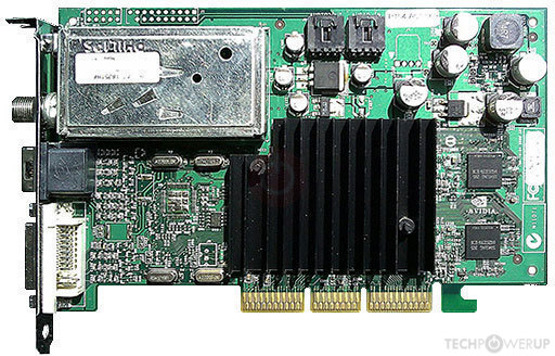
Being a single-slot card, the NVIDIA GeForce4 MX 440-SE does not require any additional power connector, its power draw is not exactly known. Display outputs include: 1x DVI, 1x VGA, 1x S-Video. GeForce4 MX 440-SE is connected to the rest of the system using an AGP 4x interface.
Being a single-slot card, the NVIDIA GeForce4 MX 440-SE does not require any additional power connector, its power draw is not exactly known. Display outputs include: 1x DVI, 1x VGA, 1x S-Video. GeForce4 MX 440-SE is connected to the rest of the system using an AGP 4x interface.
Graphics Processor
Graphics Card
- Release Date
- Feb 6th, 2002
- Generation
- GeForce 4 MX
- Predecessor
- GeForce 3
- Successor
- GeForce 4 Ti
- Production
- End-of-life
- Bus Interface
- AGP 4x
- Reviews
- 1 in our database
Clock Speeds
- GPU Clock
- 250 MHz
- Memory Clock
-
166 MHz
332 Mbps effective
Memory
- Memory Size
- 64 MB
- Memory Type
- DDR
- Memory Bus
- 128 bit
- Bandwidth
- 5.312 GB/s
Render Config
- Pixel Shaders
- 2
- Vertex Shaders
- 0
- TMUs
- 4
- ROPs
- 2
Theoretical Performance
- Pixel Rate
- 500.0 MPixel/s
- Texture Rate
- 1.000 GTexel/s
Board Design
- Slot Width
- Single-slot
- TDP
- unknown
- Suggested PSU
- 200 W
- Outputs
- 1x DVI
1x VGA
1x S-Video
- Power Connectors
- None
Graphics Features
- DirectX
- 7.0
- OpenGL
- 1.5
- OpenCL
- N/A
- Vulkan
- N/A
- Pixel Shader
- 1.1
- Vertex Shader
- 1.1
Card Notes
| Memory Variant: 128 MB |
NV17 GPU Notes
| Latest Drivers: Windows NT 4: ForceWare Release 77.56 ForceWare Release 77.72 Desktop Windows 95 / 98 / ME: ForceWare Release 81.98 Windows 2000 / XP / Server 2003 x64: ForceWare Release 93.71 Desktop ForceWare Release 91.36 / 93.81 Beta |
Retail boards based on this design (2)
| Name | GPU Clock | Memory Clock | Other Changes |
|---|---|---|---|
| 250 MHz | 166 MHz | 64 bit | |
| 250 MHz | 166 MHz | SDR |


Jul 18th, 2025 18:58 CDT
change timezone
Latest GPU Drivers
New Forum Posts
- AI Job Losses: let's count the losses up, total losses to AI so far 94,000 and counting (34)
- TPU's Nostalgic Hardware Club (20539)
- 3DMARK "LEGENDARY" (329)
- Hatsune Miku x ASUS TUF Gaming Build (67)
- What's your latest tech purchase? (24304)
- Anime Nation (13051)
- Ferrari themed mod cont. 4070s repaste (7)
- Stalker 2 is looking great. (213)
- Share your CPU-X Benchmarks! (6)
- Are UPS lithium LiFePO4 batteries finally as cheap as lead-acid? (20)
Popular Reviews
- Razer Blade 16 (2025) Review - Thin, Light, Punchy, and Efficient
- SilverStone SETA H2 Review
- Thermal Grizzly WireView Pro Review
- Pulsar X2 Crazylight Review
- MSI GeForce RTX 5060 Gaming OC Review
- Our Visit to the Hunter Super Computer
- NVIDIA GeForce RTX 5080 Founders Edition Review
- NVIDIA GeForce RTX 5050 8 GB Review
- Sapphire Radeon RX 9060 XT Pulse OC 16 GB Review - An Excellent Choice
- Upcoming Hardware Launches 2025 (Updated May 2025)
TPU on YouTube
Controversial News Posts
- Intel's Core Ultra 7 265K and 265KF CPUs Dip Below $250 (288)
- Some Intel Nova Lake CPUs Rumored to Challenge AMD's 3D V-Cache in Desktop Gaming (140)
- AMD Radeon RX 9070 XT Gains 9% Performance at 1440p with Latest Driver, Beats RTX 5070 Ti (131)
- NVIDIA Launches GeForce RTX 5050 for Desktops and Laptops, Starts at $249 (124)
- NVIDIA GeForce RTX 5080 SUPER Could Feature 24 GB Memory, Increased Power Limits (115)
- Microsoft Partners with AMD for Next-gen Xbox Hardware (105)
- NVIDIA DLSS Transformer Cuts VRAM Usage by 20% (99)
- AMD Sampling Next-Gen Ryzen Desktop "Medusa Ridge," Sees Incremental IPC Upgrade, New cIOD (97)