Report an Error


NVIDIA GA102

GA102

GA102-200-KD-A1

GA102-202-KB-A1
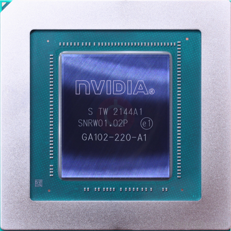
GA102-220-A1

GA102-225-A1

GA102-300-A1

GA102-350-A1

CGI Die Shot

Block Diagram

SM Diagram

DirectX 11 Support

DirectX 12 Support

DirectX 12 Support 2
NVIDIA's GA102 GPU uses the Ampere architecture and is made using a 8 nm production process at Samsung. With a die size of 628 mm² and a transistor count of 28,300 million it is a very big chip. GA102 supports DirectX 12 Ultimate (Feature Level 12_2). For GPU compute applications, OpenCL version 3.0 and CUDA 8.6 can be used. Additionally, the DirectX 12 Ultimate capability guarantees support for hardware-raytracing, variable-rate shading and more, in upcoming video games. It features 10752 shading units, 336 texture mapping units and 112 ROPs. Also included are 336 tensor cores which help improve the speed of machine learning applications. The GPU also contains 84 raytracing acceleration cores.
Further reading:
Ampere Architecture Whitepaper 
Graphics Processor
- Released
- Sep 1st, 2020
- GPU Name
- GA102
- Codename
- NV172
- Architecture
- Ampere
- Foundry
- Samsung
- Process Size
- 8 nm
- Transistors
- 28,300 million
- Density
- 45.1M / mm²
- Die Size
- 628 mm²
- Package
- BGA-3328
Graphics Features
- DirectX
- 12 Ultimate (12_2)
- DirectML
- 1.8.2 (5_0)
- OpenGL
- 4.6
- OpenCL
- 3.0
- Vulkan
- 1.3
- CUDA
- 8.6
- Shader Model
- 6.7
- WDDM
- 3.1
- Tensor Cores
- 3rd Gen
- RT Cores
- 2nd Gen
- NVENC
- 7th Gen
- NVDEC
- 5th Gen
- PureVideo HD
- VP11
- VDPAU
- Feature Set K
- Raytracing
- Tier 1.1
- VPS
- Tier 2
- Mesh Shaders
- Tier 1
Render Config
- Shading Units
- 10752
- TMUs
- 336
- ROPs
- 112
- SM Count
- 84
- FP16 Units
- 10752
- FP64 Units
- 168
- INT32 Units
- 5376
- Tensor Cores
- 336
- RT Cores
- 84
- SFUs
- 1344
- TPCs
- 42
- GPCs
- 7
- Tex L1 Cache
- 64 KB per SM
- L1 Cache
- 128 KB per SM
- L2 Cache
- 6144 KB
- Register File
- 21504 KB
- Max. TDP
- 450 W
All Ampere GPUs
NVIDIA GPU Architecture History
- 2024 Blackwell
- 2023 Hopper
- 2022-2024 Ada Lovelace
- 2020-2024 Ampere
- 2018-2022 Turing
- 2017-2020 Volta
- 2016-2021 Pascal
- 2014-2019 Maxwell 2.0
- 2014-2017 Maxwell
- 2013-2015 Kepler 2.0
- 2012-2018 Kepler
- 2010-2016 Fermi 2.0
- 2010-2013 VLIW Vec4
- 2010-2016 Fermi
- 2007-2013 Tesla 2.0
- 2006-2010 Tesla
- 2003-2013 Curie
- 2003-2005 Rankine
- 2001-2003 Kelvin
- 1999-2005 Celsius
- 1998-2000 Fahrenheit
Graphics cards using the NVIDIA GA102 GPU
| Name | Chip | Memory | Shaders | TMUs | ROPs | Base Clock | Boost Clock | Memory Clock |
|---|---|---|---|---|---|---|---|---|
| GA102-200-KD-A1 | 10 GB | 8704 | 272 | 96 | 1440 MHz | 1710 MHz | 1188 MHz | |
| GA102-300-A1 | 24 GB | 10496 | 328 | 112 | 1395 MHz | 1695 MHz | 1219 MHz | |
| 48 GB | 10752 | 336 | 112 | 1410 MHz | 1800 MHz | 2000 MHz | ||
| 48 GB | 10752 | 336 | 112 | 1305 MHz | 1740 MHz | 1812 MHz | ||
| GA102-225-A1 | 12 GB | 10240 | 320 | 112 | 1365 MHz | 1665 MHz | 1188 MHz | |
| 24 GB | 8192 | 256 | 96 | 1170 MHz | 1695 MHz | 2000 MHz | ||
| GA102-100-A1 | 10 GB | 6400 | 200 | 80 | 1500 MHz | 1710 MHz | 1188 MHz | |
| GA102-890-A1 | 24 GB | 9216 | 288 | 96 | 885 MHz | 1695 MHz | 1563 MHz | |
| GA102-890-A1 | 24 GB | 9216 | 288 | 96 | 1320 MHz | 1710 MHz | 1563 MHz | |
| GA102-350-A1 | 24 GB | 10752 | 336 | 112 | 1560 MHz | 1860 MHz | 1313 MHz | |
| GA102-225-A1 | 20 GB | 10240 | 320 | 112 | 1335 MHz | 1665 MHz | 1188 MHz | |
| GA102-220-A1 | 12 GB | 8960 | 280 | 96 | 1260 MHz | 1710 MHz | 1188 MHz | |
| 20 GB | 7168 | 224 | 96 | 1050 MHz | 1650 MHz | 2000 MHz | ||
| 24 GB | 10240 | 320 | 96 | 1080 MHz | 1665 MHz | 2000 MHz | ||
| GA102-150-A1 | 8 GB | 6144 | 192 | 96 | 1575 MHz | 1770 MHz | 1188 MHz | |
| 8 GB | 8192 | 256 | 96 | 1170 MHz | 1695 MHz | 2000 MHz | ||
| 12 GB | 8192 | 256 | 96 | 1170 MHz | 1695 MHz | 2000 MHz | ||
| 24 GB | 7168 | 224 | 80 | 975 MHz | 1635 MHz | 1563 MHz |


GA102 GPU Notes
| Ray Tracing Cores: 2nd Gen Tensor Cores: 3rd Gen NVENC: 7th Gen NVDEC: 5th Gen PureVideo HD: VP11 VDPAU: Feature Set K |
May 3rd, 2024 03:18 EDT
change timezone
Latest GPU Drivers
New Forum Posts
- Looking for recommendations to upgrade the GPU (40)
- Brother bought a house, found some old PC hardware.. (26)
- 7800x3d $216 in bundle at Microcenter (35)
- Announcement: VPN's no longer work right in Windows 10 or 11 or Servers (6)
- Ryzen Owners Zen Garden (7288)
- Need advice for UPS that will be use only for bios updates (0)
- PNY 3080 vBios (0)
- Would you guys be ok with 70C idle temp on NVME storage. (27)
- What are the consequences of genetically altering ticks, fleas, and mosquitoes to control their populations? (193)
- Locked settings in Throttlestop FIVR Dell G5 5590 (2019) (1)
Popular Reviews
- HYTE THICC Q60 240 mm AIO Review
- ASRock NUC BOX-155H (Intel Core Ultra 7 155H) Review
- Montech Sky Two GX Review
- Ugreen NASync DXP4800 Plus Review
- Meze Audio LIRIC 2nd Generation Closed-Back Headphones Review
- Upcoming Hardware Launches 2023 (Updated Feb 2024)
- Team Group T-Force Vulcan ECO DDR5-6000 32 GB CL38 Review
- MOONDROP x Crinacle DUSK In-Ear Monitors Review - The Last 5%
- AMD Ryzen 7 7800X3D Review - The Best Gaming CPU
- Logitech G Pro X Superlight 2 Review - Updated with 4000 Hz Tested
Controversial News Posts
- Intel Statement on Stability Issues: "Motherboard Makers to Blame" (230)
- Windows 11 Now Officially Adware as Microsoft Embeds Ads in the Start Menu (167)
- Sony PlayStation 5 Pro Specifications Confirmed, Console Arrives Before Holidays (117)
- AMD's RDNA 4 GPUs Could Stick with 18 Gbps GDDR6 Memory (114)
- NVIDIA Points Intel Raptor Lake CPU Users to Get Help from Intel Amid System Instability Issues (106)
- AMD "Strix Halo" Zen 5 Mobile Processor Pictured: Chiplet-based, Uses 256-bit LPDDR5X (103)
- AMD Ryzen 9 7900X3D Now at a Mouth-watering $329 (103)
- TechPowerUp Hiring: Reviewers Wanted for Motherboards, Laptops, Gaming Handhelds and Prebuilt Desktops (93)