Report an Error


NVIDIA GK208B
GK208B
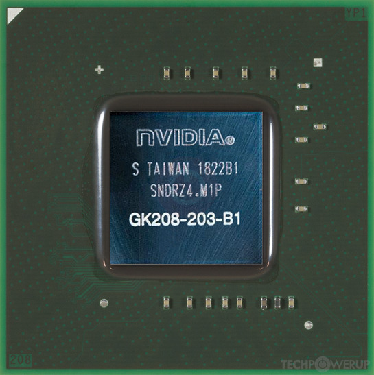
GK208-203-B1

GK208-302-B1

Block Diagram
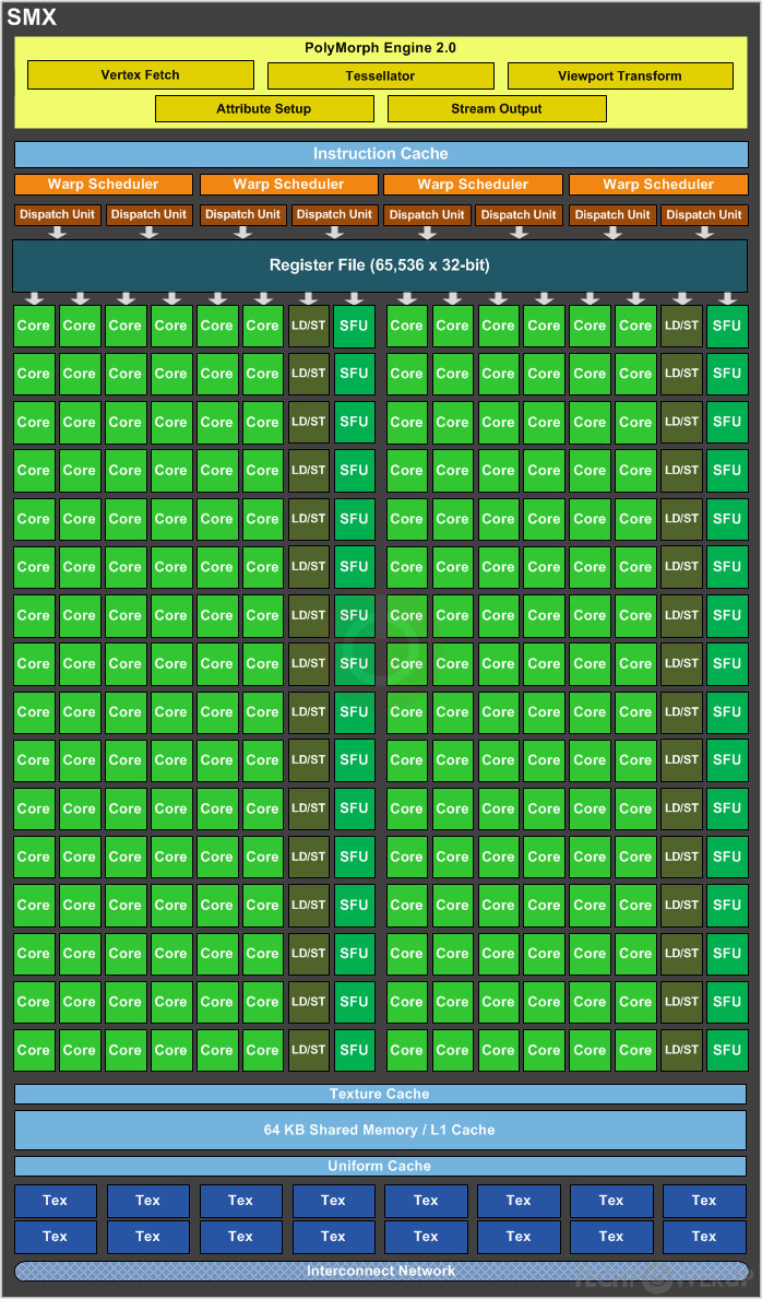
SMX Diagram
NVIDIA's GK208B GPU uses the Kepler 2.0 architecture and is made using a 28 nm production process at TSMC. With a die size of 87 mm² and a transistor count of 1,020 million it is a very small chip. GK208B supports DirectX 12 (Feature Level 11_0). For GPU compute applications, OpenCL version 3.0 and CUDA 3.5 can be used. It features 384 shading units, 32 texture mapping units and 8 ROPs.
Graphics Processor
- Released
- Mar 27th, 2014
- GPU Name
- GK208B
- Codename
- NV106
- Architecture
- Kepler 2.0
- Foundry
- TSMC
- Process Size
- 28 nm
- Transistors
- 1,020 million
- Density
- 11.7M / mm²
- Die Size
- 87 mm²
- Package
- FCBGA-595
Graphics Features
- DirectX
- 12 (11_0)
- OpenGL
- 4.6
- OpenCL
- 3.0
- Vulkan
- 1.2.175
- CUDA
- 3.5
- Shader Model
- 6.5 (5.1)
- WDDM
- 3.0
- NVENC
- No Support
- NVDEC
- 1st Gen
- PureVideo HD
- VP5
- VDPAU
- Feature Set D
Render Config
- Shading Units
- 384
- TMUs
- 32
- ROPs
- 8
- SMX Count
- 2
- GPCs
- 1
- Tex L1 Cache
- 48 KB per SMX
- L1 Cache
- 16 KB per SMX
- L2 Cache
- 512 KB
- Max. TDP
- 38 W
- SFUs
- 64
All Kepler 2.0 GPUs
- NVIDIA GK208
- NVIDIA GK208B
- NVIDIA GK20A
- NVIDIA GK210
NVIDIA GPU Architecture History
- 2024 Blackwell
- 2023 Hopper
- 2022-2024 Ada Lovelace
- 2020-2024 Ampere
- 2018-2022 Turing
- 2017-2020 Volta
- 2016-2021 Pascal
- 2014-2019 Maxwell 2.0
- 2014-2017 Maxwell
- 2013-2015 Kepler 2.0
- 2012-2018 Kepler
- 2010-2016 Fermi 2.0
- 2010-2013 VLIW Vec4
- 2010-2016 Fermi
- 2007-2013 Tesla 2.0
- 2006-2010 Tesla
- 2003-2013 Curie
- 2003-2005 Rankine
- 2001-2003 Kelvin
- 1999-2005 Celsius
- 1998-2000 Fahrenheit
Graphics cards using the NVIDIA GK208B GPU
| Name | Chip | Memory | Shaders | TMUs | ROPs | GPU Clock | Memory Clock |
|---|---|---|---|---|---|---|---|
| GK208-302-B1 | 1024 MB | 384 | 32 | 8 | 902 MHz | 1253 MHz | |
| GK208-203-B1 | 2 GB | 192 | 16 | 8 | 954 MHz | 900 MHz | |
| N16V-GM-B1 | 2 GB | 384 | 32 | 8 | 954 MHz | 900 MHz | |
| N16V-GM | 1024 MB | 384 | 32 | 8 | 954 MHz | 1001 MHz | |
| 1024 MB | 192 | 16 | 8 | 797 MHz | 800 MHz | ||
| 1024 MB | 192 | 16 | 8 | 797 MHz | 900 MHz | ||
| N16V-GL | 2 GB | 384 | 32 | 8 | 641 MHz | 1001 MHz | |
| GK208-203-B1 | 1024 MB | 192 | 16 | 8 | 954 MHz | 800 MHz |


GK208B GPU Notes
| NVENC: No Support NVDEC: 1st Gen PureVideo HD: VP5 VDPAU: Feature Set D L1 Cache is configurable from 16 KB up to 48 KB per SMX |
May 18th, 2024 22:26 EDT
change timezone
Latest GPU Drivers
New Forum Posts
- EK seems to be having major issues (104)
- What are you playing? (20700)
- I make new budgeout build. Tell me ,where i dont see wrong choices... (9)
- Blender 3.3.0 Benchmark (13)
- Post your 7-Zip v22.01 scores (343)
- Overclock AMD Ryzen 9 5900X On ROG STRIX B550-A GAMING After New Bios Update. (2)
- AM5 boot times improve RADICALLY with memory context restore enabled (87)
- What's your latest tech purchase? (20565)
- Windows 7 and Gigabyte 299x wu8 (4)
- AMD Radeon Pro v540 Research Thread (257)
Popular Reviews
- Ghost of Tsushima Performance Benchmark Review - 35 GPUs Tested
- Homeworld 3 Performance Benchmark Review - 35 GPUs Tested
- Lofree Edge Ultra-Low Profile Wireless Mechanical Keyboard Review
- Silverstone Shark Force 120 mm Fan Review
- Enermax REVOLUTION D.F. X 1200 W Review
- TerraMaster D8 Hybrid Review
- Upcoming Hardware Launches 2023 (Updated Feb 2024)
- AMD Ryzen 7 7800X3D Review - The Best Gaming CPU
- AMD Radeon RX 7900 XTX Review - Disrupting the GeForce RTX 4080
- Sapphire Radeon RX 7900 GRE Pulse Review
Controversial News Posts
- Intel Statement on Stability Issues: "Motherboard Makers to Blame" (269)
- AMD to Redesign Ray Tracing Hardware on RDNA 4 (227)
- Windows 11 Now Officially Adware as Microsoft Embeds Ads in the Start Menu (172)
- NVIDIA to Only Launch the Flagship GeForce RTX 5090 in 2024, Rest of the Series in 2025 (154)
- AMD Hits Highest-Ever x86 CPU Market Share in Q1 2024 Across Desktop and Server (139)
- AMD RDNA 5 a "Clean Sheet" Graphics Architecture, RDNA 4 Merely Corrects a Bug Over RDNA 3 (130)
- AMD's RDNA 4 GPUs Could Stick with 18 Gbps GDDR6 Memory (114)
- AMD Ryzen 9 7900X3D Now at a Mouth-watering $329 (104)