Report an Error


NVIDIA GM107

GM107
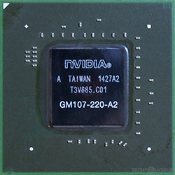
GM107-220-A2

GM107-300-A2

GM107-400-A2

GM107-850-A2

GM107-860-A2

N16P-Q1-A2

GM107 BGA
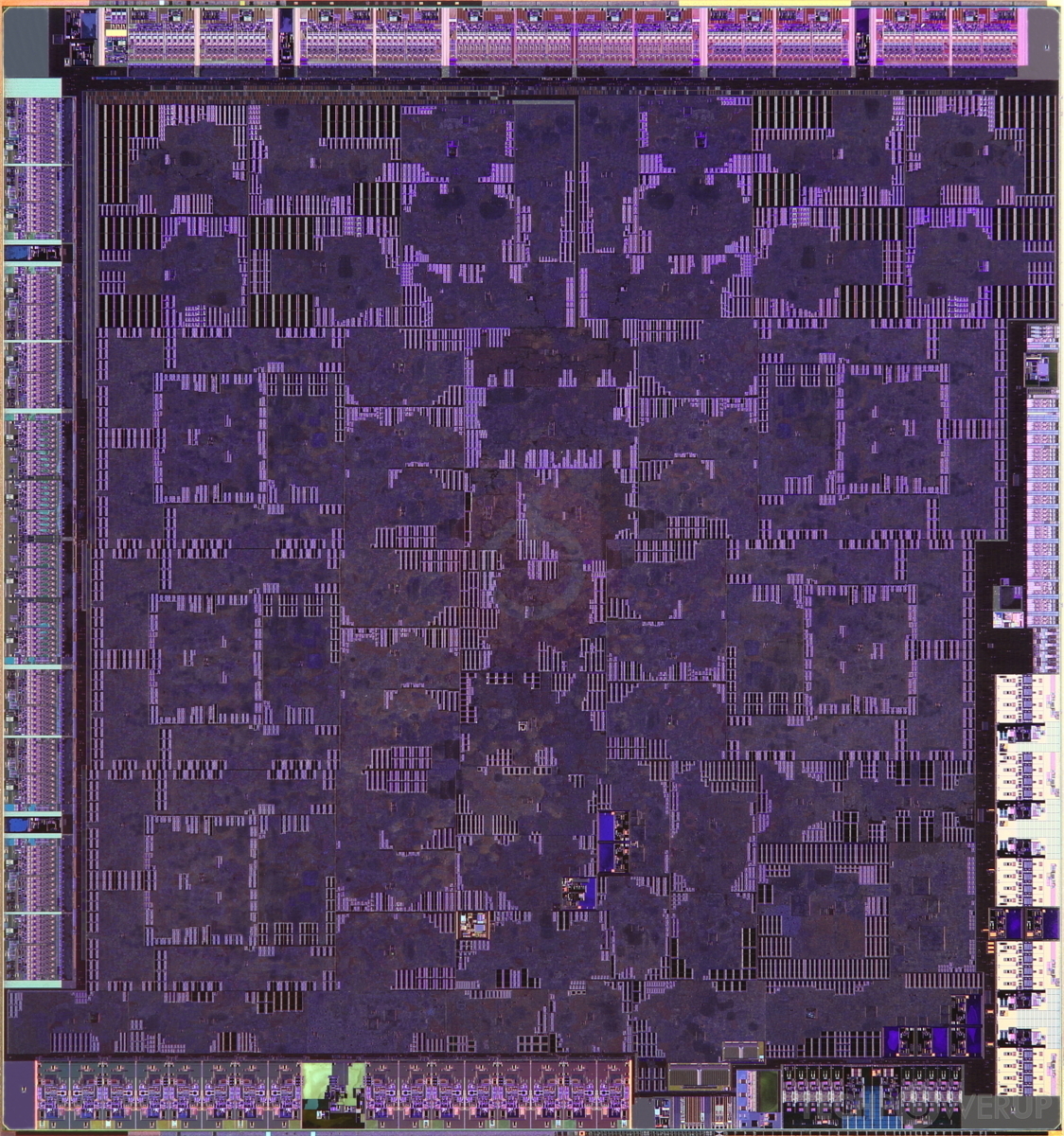
Die Shot

Block Diagram

SMM Diagram
NVIDIA's GM107 GPU uses the Maxwell architecture and is made using a 28 nm production process at TSMC. With a die size of 148 mm² and a transistor count of 1,870 million it is a small chip. GM107 supports DirectX 12 (Feature Level 11_0). For GPU compute applications, OpenCL version 3.0 and CUDA 5.0 can be used. It features 640 shading units, 40 texture mapping units and 16 ROPs.
Further reading:
GM107 Architecture Whitepaper 
Graphics Processor
- Released
- Jan 13th, 2014
- GPU Name
- GM107
- Codename
- NV117
- Architecture
- Maxwell
- Foundry
- TSMC
- Process Size
- 28 nm
- Transistors
- 1,870 million
- Density
- 12.6M / mm²
- Die Size
- 148 mm²
- Package
- FCBGA-908
Graphics Features
- DirectX
- 12 (11_0)
- OpenGL
- 4.6
- OpenCL
- 3.0
- Vulkan
- 1.3
- CUDA
- 5.0
- Shader Model
- 6.7 (5.1)
- WDDM
- 3.1
- NVENC
- 4th Gen
- NVDEC
- 1st Gen
- PureVideo HD
- VP6
- VDPAU
- Feature Set E
Render Config
- Shading Units
- 640
- TMUs
- 40
- ROPs
- 16
- SMM Count
- 5
- GPCs
- 1
- L1 Cache
- 64 KB per SMM
- L2 Cache
- 2048 KB
- Max. TDP
- 225 W
- SFUs
- 160
All Maxwell GPUs
- NVIDIA GM107
- NVIDIA GM108
- NVIDIA GM108S
NVIDIA GPU Architecture History
- 2024 Blackwell
- 2023 Hopper
- 2022-2024 Ada Lovelace
- 2020-2024 Ampere
- 2018-2022 Turing
- 2017-2020 Volta
- 2016-2021 Pascal
- 2014-2019 Maxwell 2.0
- 2014-2017 Maxwell
- 2013-2015 Kepler 2.0
- 2012-2018 Kepler
- 2010-2016 Fermi 2.0
- 2010-2013 VLIW Vec4
- 2010-2016 Fermi
- 2007-2013 Tesla 2.0
- 2006-2010 Tesla
- 2003-2013 Curie
- 2003-2005 Rankine
- 2001-2003 Kelvin
- 1999-2005 Celsius
- 1998-2000 Fahrenheit
Graphics cards using the NVIDIA GM107 GPU
| Name | Chip | Memory | Shaders | TMUs | ROPs | Base Clock | Boost Clock | Memory Clock |
|---|---|---|---|---|---|---|---|---|
| GM107-300-A2 | 1024 MB | 512 | 32 | 16 | 1020 MHz | 1085 MHz | 1253 MHz | |
| 8 GB | 384 | 32 | 16 | 1033 MHz | 1300 MHz | |||
| N15P-GX-A1 | 2 GB | 640 | 40 | 16 | 1020 MHz | 1020 MHz | 1253 MHz | |
| N15P-GT-A1 | 2 GB | 640 | 40 | 16 | 902 MHz | 1001 MHz | ||
| GM107-400-A2 | 2 GB | 640 | 40 | 16 | 1020 MHz | 1085 MHz | 1350 MHz | |
| GM107-220-A2 | 4 GB | 384 | 24 | 16 | 1033 MHz | 900 MHz | ||
| N15P-GT-A1 | 2 GB | 640 | 40 | 16 | 902 MHz | 902 MHz | 900 MHz | |
| 2 GB | 640 | 40 | 16 | 1150 MHz | 1150 MHz | 1253 MHz | ||
| GM107-850-A2 | 2 GB | 384 | 24 | 16 | 1058 MHz | 1124 MHz | 900 MHz | |
| 4 GB | 640 | 40 | 16 | 1046 MHz | 1124 MHz | 1253 MHz | ||
| N16P-GX-A1 | 4 GB | 640 | 40 | 16 | 1097 MHz | 1176 MHz | 1253 MHz | |
| GM107-860-A2 | 4 GB | 512 | 32 | 16 | 1058 MHz | 1124 MHz | 1250 MHz | |
| N16P-GT | 4 GB | 640 | 40 | 16 | 993 MHz | 1124 MHz | 900 MHz | |
| N16S-GT1-KB-B | 2 GB | 512 | 32 | 16 | 1020 MHz | 1098 MHz | 900 MHz | |
| N15P-GX-A1 | 2 GB | 640 | 40 | 16 | 1097 MHz | 1176 MHz | 1253 MHz | |
| N15S-GT1R-KA-A2 | 2 GB | 512 | 32 | 16 | 863 MHz | 863 MHz | 1001 MHz | |
| 2 GB | 384 | 16 | 8 | 837 MHz | 876 MHz | 1253 MHz | ||
| N16P-Q1-A2 | 2 GB | 512 | 32 | 16 | 993 MHz | 1072 MHz | 1253 MHz | |
| N16P-Q3-A2 | 4 GB | 640 | 40 | 16 | 1098 MHz | 1137 MHz | 1253 MHz | |
| 2 GB | 512 | 32 | 16 | 902 MHz | 1033 MHz | 900 MHz | ||
| 2 GB | 640 | 40 | 16 | 928 MHz | 1020 MHz | 900 MHz | ||
| N16P-GX-A1 | 2 GB | 640 | 40 | 16 | 1097 MHz | 1176 MHz | 1253 MHz | |
| N16P-GT | 2 GB | 640 | 40 | 16 | 993 MHz | 1124 MHz | 1001 MHz | |
| N16P-GT | 2 GB | 640 | 40 | 16 | 993 MHz | 1124 MHz | 900 MHz | |
| N16S-GT1R | 2 GB | 512 | 32 | 8 | 795 MHz | 861 MHz | 1253 MHz | |
| 2 GB | 512 | 32 | 16 | 756 MHz | 1018 MHz | 1253 MHz | ||
| 4 GB | 640 | 40 | 16 | 991 MHz | 1148 MHz | 1253 MHz | ||
| GM107-570-A2 | 8 GB | 640 | 40 | 16 | 1033 MHz | 1306 MHz | 1300 MHz | |
| 4 GB | 640 | 40 | 16 | 1033 MHz | 1306 MHz | 1300 MHz | ||
| GM107-570-A2 | 8 GB | 640 | 40 | 16 | 1033 MHz | 1306 MHz | 1300 MHz |


GM107 GPU Notes
| NVENC: 4th Gen NVDEC: 1st Gen PureVideo HD: VP6 VDPAU: Feature Set E |
May 3rd, 2024 05:09 EDT
change timezone
Latest GPU Drivers
New Forum Posts
- Just for lolz, Post your 3DMark2001SE Benchmark scores! (83)
- Which PSU to take? (41)
- Old high quality PSU, or semi-old mid-quality PSU? (48)
- Arctic MX-6 shelf life is just a couple months? (79)
- 7800x3d $216 in bundle at Microcenter (36)
- What are the consequences of genetically altering ticks, fleas, and mosquitoes to control their populations? (194)
- Why does my PC shut down even though it's connected to a UPS? (75)
- PNY 3080 vBios (1)
- Looking for recommendations to upgrade the GPU (40)
- Brother bought a house, found some old PC hardware.. (26)
Popular Reviews
- HYTE THICC Q60 240 mm AIO Review
- ASRock NUC BOX-155H (Intel Core Ultra 7 155H) Review
- Montech Sky Two GX Review
- Meze Audio LIRIC 2nd Generation Closed-Back Headphones Review
- Ugreen NASync DXP4800 Plus Review
- Upcoming Hardware Launches 2023 (Updated Feb 2024)
- Team Group T-Force Vulcan ECO DDR5-6000 32 GB CL38 Review
- MOONDROP x Crinacle DUSK In-Ear Monitors Review - The Last 5%
- AMD Ryzen 7 7800X3D Review - The Best Gaming CPU
- Logitech G Pro X Superlight 2 Review - Updated with 4000 Hz Tested
Controversial News Posts
- Intel Statement on Stability Issues: "Motherboard Makers to Blame" (231)
- Windows 11 Now Officially Adware as Microsoft Embeds Ads in the Start Menu (167)
- Sony PlayStation 5 Pro Specifications Confirmed, Console Arrives Before Holidays (117)
- AMD's RDNA 4 GPUs Could Stick with 18 Gbps GDDR6 Memory (114)
- NVIDIA Points Intel Raptor Lake CPU Users to Get Help from Intel Amid System Instability Issues (106)
- AMD "Strix Halo" Zen 5 Mobile Processor Pictured: Chiplet-based, Uses 256-bit LPDDR5X (103)
- AMD Ryzen 9 7900X3D Now at a Mouth-watering $329 (103)
- TechPowerUp Hiring: Reviewers Wanted for Motherboards, Laptops, Gaming Handhelds and Prebuilt Desktops (93)