Report an Error


NVIDIA Quadro GV100
- Graphics Processor
- GV100
- Cores
- 5120
- TMUs
- 320
- ROPs
- 128
- Memory Size
- 32 GB
- Memory Type
- HBM2
- Bus Width
- 4096 bit
GPU

I/O

Top

Rear

Back
Recommended Gaming Resolutions:
- 1920x1080
- 2560x1440
- 3840x2160
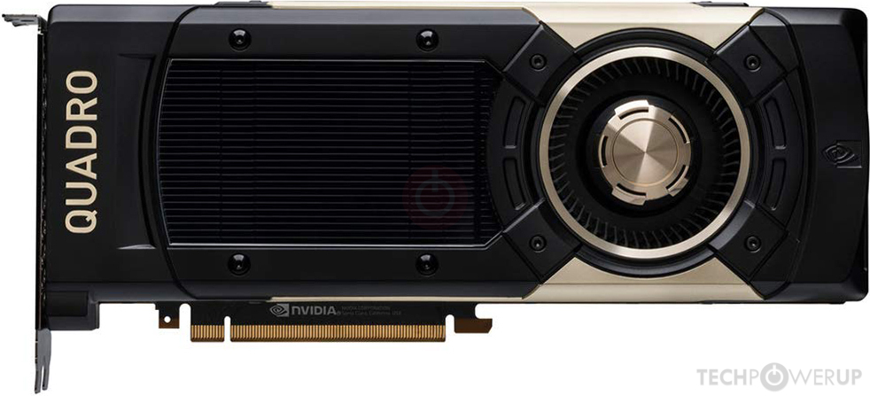
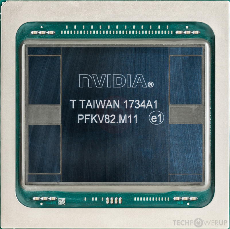
The Quadro GV100 was an enthusiast-class professional graphics card by NVIDIA, launched on March 27th, 2018. Built on the 12 nm process, and based on the GV100 graphics processor, in its GV100-875-A1 variant, the card supports DirectX 12. The GV100 graphics processor is a large chip with a die area of 815 mm² and 21,100 million transistors. It features 5120 shading units, 320 texture mapping units, and 128 ROPs. Also included are 640 tensor cores which help improve the speed of machine learning applications. NVIDIA has paired 32 GB HBM2 memory with the Quadro GV100, which are connected using a 4096-bit memory interface. The GPU is operating at a frequency of 1132 MHz, which can be boosted up to 1627 MHz, memory is running at 848 MHz.
Being a dual-slot card, the NVIDIA Quadro GV100 draws power from 1x 8-pin power connector, with power draw rated at 250 W maximum. Display outputs include: 4x DisplayPort 1.4a. Quadro GV100 is connected to the rest of the system using a PCI-Express 3.0 x16 interface. The card measures 267 mm in length, 111 mm in width, and features a dual-slot cooling solution. Its price at launch was 8999 US Dollars.
Being a dual-slot card, the NVIDIA Quadro GV100 draws power from 1x 8-pin power connector, with power draw rated at 250 W maximum. Display outputs include: 4x DisplayPort 1.4a. Quadro GV100 is connected to the rest of the system using a PCI-Express 3.0 x16 interface. The card measures 267 mm in length, 111 mm in width, and features a dual-slot cooling solution. Its price at launch was 8999 US Dollars.
Graphics Processor
Graphics Card
- Release Date
- Mar 27th, 2018
- Generation
-
Quadro Volta
(Vx000)
- Predecessor
- Quadro Pascal
- Successor
- Quadro Turing
- Production
- End-of-life
- Launch Price
- 8,999 USD
- Bus Interface
- PCIe 3.0 x16
Relative Performance
Based on TPU review data: "Performance Summary" at 1920x1080, 4K for 2080 Ti and faster.
Performance estimated based on architecture, shader count and clocks.
Clock Speeds
- Base Clock
- 1132 MHz
- Boost Clock
- 1627 MHz
- Memory Clock
-
848 MHz
1696 Mbps effective
Memory
- Memory Size
- 32 GB
- Memory Type
- HBM2
- Memory Bus
- 4096 bit
- Bandwidth
- 868.4 GB/s
Render Config
- Shading Units
- 5120
- TMUs
- 320
- ROPs
- 128
- SM Count
- 80
- Tensor Cores
- 640
- L1 Cache
- 128 KB (per SM)
- L2 Cache
- 6 MB
Theoretical Performance
- Pixel Rate
- 208.3 GPixel/s
- Texture Rate
- 520.6 GTexel/s
- FP16 (half)
- 33.32 TFLOPS (2:1)
- FP32 (float)
- 16.66 TFLOPS
- FP64 (double)
- 8.330 TFLOPS (1:2)
Board Design
- Slot Width
- Dual-slot
- Length
- 267 mm
10.5 inches
- Width
- 111 mm
4.4 inches
- TDP
- 250 W
- Suggested PSU
- 600 W
- Outputs
- 4x DisplayPort 1.4a
- Power Connectors
- 1x 8-pin
- Board Number
- PG500 SKU 500
Graphics Features
- DirectX
- 12 (12_1)
- OpenGL
- 4.6
- OpenCL
- 3.0
- Vulkan
- 1.3
- CUDA
- 7.0
- Shader Model
- 6.7
Card Notes
| Base Clock: Deep Learning: 92.733TFLOPs Boost Clock: Deep Learning: 133.365TFLOPs |
GV100 GPU Notes
| Tensor Cores: 1st Gen NVENC: 6th Gen NVDEC: 3rd Gen PureVideo HD: VP9 VDPAU: Feature Set I |
May 21st, 2024 09:11 EDT
change timezone
Latest GPU Drivers
New Forum Posts
- Ryzen 5 5600x stock overclocked reaching high temps (12)
- What's your latest tech purchase? (20607)
- My anti budget PC (60)
- What are you playing? (20722)
- MSI RX 580 Armor 8GB VBios (2)
- LG OLED C1 TV odd behaviour after nearly 2 years (57)
- Does a faster NVMe make any difference? (18)
- Would you pay more for hardware with AI capabilities? (51)
- Dell 5400 TPL Help (5)
- EK seems to be having major issues (126)
Popular Reviews
- Ghost of Tsushima Performance Benchmark Review - 35 GPUs Tested
- Ghost of Tsushima: DLSS vs. FSR vs. XeSS Comparison Review
- PNY XLR8 Gaming EPIC-X RGB DDR5-6400 CL32 32 GB Review
- TerraMaster D8 Hybrid Review
- Silverstone Shark Force 120 mm Fan Review
- Homeworld 3 Performance Benchmark Review - 35 GPUs Tested
- Upcoming Hardware Launches 2023 (Updated Feb 2024)
- Lofree Edge Ultra-Low Profile Wireless Mechanical Keyboard Review
- AMD Ryzen 7 7800X3D Review - The Best Gaming CPU
- AMD Ryzen 7 7700 Review - Affordable Zen 4 Powerhouse
Controversial News Posts
- Intel Statement on Stability Issues: "Motherboard Makers to Blame" (269)
- AMD to Redesign Ray Tracing Hardware on RDNA 4 (227)
- Windows 11 Now Officially Adware as Microsoft Embeds Ads in the Start Menu (173)
- NVIDIA to Only Launch the Flagship GeForce RTX 5090 in 2024, Rest of the Series in 2025 (154)
- AMD Hits Highest-Ever x86 CPU Market Share in Q1 2024 Across Desktop and Server (140)
- AMD RDNA 5 a "Clean Sheet" Graphics Architecture, RDNA 4 Merely Corrects a Bug Over RDNA 3 (139)
- AMD's RDNA 4 GPUs Could Stick with 18 Gbps GDDR6 Memory (114)
- AMD Ryzen 9 7900X3D Now at a Mouth-watering $329 (104)