Report an Error


NVIDIA Quadro RTX 5000 X2 Mobile
- Graphics Processor
- TU104 x2
- Cores
- 3072 x2
- TMUs
- 192 x2
- ROPs
- 64 x2
- Memory Size
- 16 GB x2
- Memory Type
- GDDR6
- Bus Width
- 256 bit x2
GPU
Recommended Gaming Resolutions:
- 1920x1080
- 2560x1440
- 3840x2160
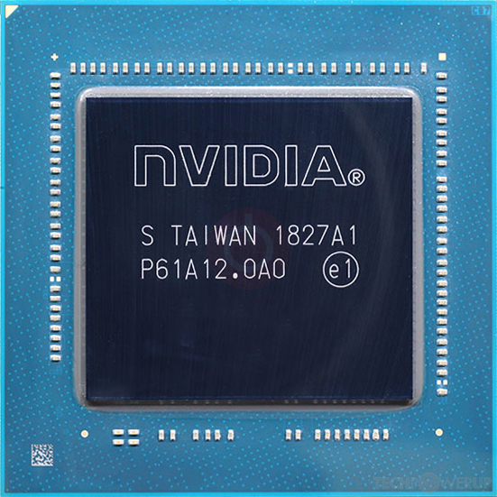
The Quadro RTX 5000 X2 Mobile is a professional mobile graphics chip by NVIDIA, launched on June 8th, 2020. Built on the 12 nm process, and based on the TU104 graphics processor, in its N19E-Q5-A1 variant, the chip supports DirectX 12 Ultimate. The TU104 graphics processor is a large chip with a die area of 545 mm² and 13,600 million transistors. Quadro RTX 5000 X2 Mobile combines two graphics processors to increase performance. It features 3072 shading units, 192 texture mapping units, and 64 ROPs, per GPU. Also included are 384 tensor cores which help improve the speed of machine learning applications. The card also has 48 raytracing acceleration cores. NVIDIA has paired 32 GB GDDR6 memory with the Quadro RTX 5000 X2 Mobile, which are connected using a 256-bit memory interface per GPU (each GPU manages 16,384 MB). The GPU is operating at a frequency of 1035 MHz, which can be boosted up to 1530 MHz, memory is running at 1750 MHz (14 Gbps effective).
Its power draw is rated at 110 W maximum. This device has no display connectivity, as it is not designed to have monitors connected to it. Rather it is intended for use in laptop/notebooks and will use the output of the host mobile device. Quadro RTX 5000 X2 Mobile is connected to the rest of the system using a PCI-Express 3.0 x16 interface.
Its power draw is rated at 110 W maximum. This device has no display connectivity, as it is not designed to have monitors connected to it. Rather it is intended for use in laptop/notebooks and will use the output of the host mobile device. Quadro RTX 5000 X2 Mobile is connected to the rest of the system using a PCI-Express 3.0 x16 interface.
Graphics Processor
Mobile Graphics
- Release Date
- Jun 8th, 2020
- Generation
-
Quadro Turing-M
(Tx000)
- Predecessor
- Quadro Pascal-M
- Successor
- Quadro Ampere-M
- Production
- Active
- Bus Interface
- PCIe 3.0 x16
Relative Performance
Based on TPU review data: "Performance Summary" at 1920x1080, 4K for 2080 Ti and faster.
Performance estimated based on architecture, shader count and clocks.
Clock Speeds
- Base Clock
- 1035 MHz
- Boost Clock
- 1530 MHz
- Memory Clock
-
1750 MHz
14 Gbps effective
Memory
- Memory Size
- 16 GB
- Memory Type
- GDDR6
- Memory Bus
- 256 bit
- Bandwidth
- 448.0 GB/s
Render Config
- Shading Units
- 3072
- TMUs
- 192
- ROPs
- 64
- SM Count
- 48
- Tensor Cores
- 384
- RT Cores
- 48
- L1 Cache
- 64 KB (per SM)
- L2 Cache
- 4 MB
Theoretical Performance
- Pixel Rate
- 97.92 GPixel/s
- Texture Rate
- 293.8 GTexel/s
- FP16 (half)
- 18.80 TFLOPS (2:1)
- FP32 (float)
- 9.400 TFLOPS
- FP64 (double)
- 293.8 GFLOPS (1:32)
Board Design
- Slot Width
- IGP
- TDP
- 110 W
- Outputs
- Portable Device Dependent
- Power Connectors
- None
Graphics Features
- DirectX
- 12 Ultimate (12_2)
- OpenGL
- 4.6
- OpenCL
- 3.0
- Vulkan
- 1.3
- CUDA
- 7.5
- Shader Model
- 6.7
TU104 GPU Notes
| Ray Tracing Cores: 1st Gen Tensor Cores: 2nd Gen NVENC: 7th Gen NVDEC: 4th Gen PureVideo HD: VP10 VDPAU: Feature Set J |
Devices based on this design (3)
| Name | GPU Clock | Boost Clock | Memory Clock | Other Changes |
|---|---|---|---|---|
| 1035 MHz | 1530 MHz | 1750 MHz | ||
| 1035 MHz | 1530 MHz | 1750 MHz | ||
| 1365 MHz | 1770 MHz | 1750 MHz | 4x mini-DisplayPort |


May 21st, 2024 22:08 EDT
change timezone
Latest GPU Drivers
New Forum Posts
- Gigabyte am5 motherboard ddr5 not posting when rebooting (10)
- In what order do you update a new install of Win11? (4)
- PNY RTX 4070 Ti XLR8 OC - New worse BIOS/version? (111)
- Been away from PC gaming, a bit lost... (9)
- Free Games Thread (3824)
- What's your latest tech purchase? (20621)
- Post Your TIMESPY, PCMARK10 & FIRESTRIKE SCORES! (2019) (230)
- 3DMARK "LEGENDARY" (197)
- Post your cooling. (10)
- Can't set PROCHOT offset (1)
Popular Reviews
- Ghost of Tsushima Performance Benchmark Review - 35 GPUs Tested
- Ghost of Tsushima: DLSS vs. FSR vs. XeSS Comparison Review
- PNY XLR8 Gaming EPIC-X RGB DDR5-6400 CL32 32 GB Review
- AMD Ryzen 7 7800X3D Review - The Best Gaming CPU
- TerraMaster D8 Hybrid Review
- CHERRY XTRFY M68 Pro Review
- Senua's Saga: Hellblade II Performance Benchmark Review
- Upcoming Hardware Launches 2023 (Updated Feb 2024)
- Homeworld 3 Performance Benchmark Review - 35 GPUs Tested
- Silverstone Shark Force 120 mm Fan Review
Controversial News Posts
- Intel Statement on Stability Issues: "Motherboard Makers to Blame" (269)
- AMD to Redesign Ray Tracing Hardware on RDNA 4 (227)
- Windows 11 Now Officially Adware as Microsoft Embeds Ads in the Start Menu (173)
- NVIDIA to Only Launch the Flagship GeForce RTX 5090 in 2024, Rest of the Series in 2025 (154)
- AMD Hits Highest-Ever x86 CPU Market Share in Q1 2024 Across Desktop and Server (140)
- AMD RDNA 5 a "Clean Sheet" Graphics Architecture, RDNA 4 Merely Corrects a Bug Over RDNA 3 (139)
- AMD's RDNA 4 GPUs Could Stick with 18 Gbps GDDR6 Memory (114)
- AMD Ryzen 9 7900X3D Now at a Mouth-watering $329 (104)