Report an Error


NVIDIA GeForce GT 330 OEM
- Graphics Processor
- GT215
- Cores
- 96
- TMUs
- 32
- ROPs
- 8
- Memory Size
- 512 MB
- Memory Type
- GDDR3
- Bus Width
- 128 bit
GPU
Recommended Gaming Resolutions:
- 640x480
- 1280x720
- 1366x768
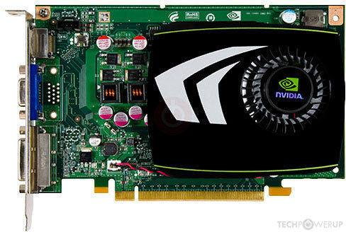
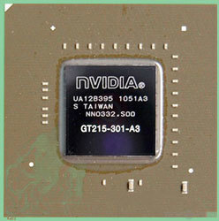
The GeForce GT 330 OEM was a graphics card by NVIDIA, launched on February 2nd, 2010. Built on the 40 nm process, and based on the GT215 graphics processor, in its GT215-301-A3 variant, the card supports DirectX 11.1. Even though it supports DirectX 11, the feature level is only 10_1, which can be problematic with many DirectX 11 & DirectX 12 titles. The GT215 graphics processor is an average sized chip with a die area of 144 mm² and 727 million transistors. It features 96 shading units, 32 texture mapping units, and 8 ROPs. NVIDIA has paired 512 MB GDDR3 memory with the GeForce GT 330 OEM, which are connected using a 128-bit memory interface. The GPU is operating at a frequency of 550 MHz, memory is running at 1000 MHz.
Being a single-slot card, the NVIDIA GeForce GT 330 OEM does not require any additional power connector, its power draw is rated at 75 W maximum. Display outputs include: 1x DVI, 1x HDMI, 1x VGA. GeForce GT 330 OEM is connected to the rest of the system using a PCI-Express 2.0 x16 interface. The card measures 175 mm in length, and features a single-slot cooling solution.
Being a single-slot card, the NVIDIA GeForce GT 330 OEM does not require any additional power connector, its power draw is rated at 75 W maximum. Display outputs include: 1x DVI, 1x HDMI, 1x VGA. GeForce GT 330 OEM is connected to the rest of the system using a PCI-Express 2.0 x16 interface. The card measures 175 mm in length, and features a single-slot cooling solution.
Graphics Processor
Graphics Card
- Release Date
- Feb 2nd, 2010
- Generation
- GeForce 300
- Predecessor
- GeForce 200
- Successor
- GeForce 400
- Production
- End-of-life
- Bus Interface
- PCIe 2.0 x16
Relative Performance
Based on TPU review data: "Performance Summary" at 1920x1080, 4K for 2080 Ti and faster.
Performance estimated based on architecture, shader count and clocks.
Clock Speeds
- GPU Clock
- 550 MHz
- Shader Clock
- 1340 MHz
- Memory Clock
-
1000 MHz
2 Gbps effective
Memory
- Memory Size
- 512 MB
- Memory Type
- GDDR3
- Memory Bus
- 128 bit
- Bandwidth
- 32.00 GB/s
Render Config
- Shading Units
- 96
- TMUs
- 32
- ROPs
- 8
- SM Count
- 12
- L2 Cache
- 64 KB
Theoretical Performance
- Pixel Rate
- 4.400 GPixel/s
- Texture Rate
- 17.60 GTexel/s
- FP32 (float)
- 257.3 GFLOPS
Board Design
- Slot Width
- Single-slot
- Length
- 175 mm
6.9 inches
- TDP
- 75 W
- Suggested PSU
- 250 W
- Outputs
- 1x DVI
1x HDMI
1x VGA
- Power Connectors
- None
- Board Number
- P681 SKU 11
Graphics Features
- DirectX
- 11.1 (10_1)
- OpenGL
- 3.3
- OpenCL
- 1.1
- Vulkan
- N/A
- CUDA
- 1.2
- Shader Model
- 4.1
Card Notes
| Memory Variant: 1 GB |
GT215 GPU Notes
| PureVideo HD: VP4 VDPAU: Feature Set C Latest Drivers: Windows 2000: Quadro Release 261.19 Windows XP / Server 2003 x64: GeForce Release 185.81 (Notebooks) GeForce Release 340.52 Quadro Release R319 U2 (321.01) Tesla Release 258.96 Windows Vista: GeForce Release 307.83 (Notebooks) GeForce Release 342.01 Quadro Release R340 U15 (342.01) Tesla Release 258.96 Windows 7 / 8 / 8.1 / 10: GeForce Release 342.01 Quadro Release R340 U15 (342.01) Tesla Release 258.96 |
Retail boards based on this design (1)
| Name | GPU Clock | Memory Clock | Other Changes |
|---|---|---|---|
| 550 MHz | 790 MHz | 1024 MB, DDR3, 1x DVI 1x DisplayPort |

Apr 14th, 2025 15:40 EDT
change timezone
Latest GPU Drivers
New Forum Posts
- Milestones (14018)
- maxsun rx590* vbios (15)
- Have you got pie today? (16664)
- Linux and Intel Arc B570/B580 GPU Hardware Transcoding: What am I missing? (3)
- Gainward Phoenix RTX 5070ti Temperatures (7)
- WCG Daily Numbers (12837)
- Zenless Zone Zero artifacts on Nvidia GPU not on AMD one (4)
- TPU's Rosetta Milestones and Daily Pie Thread (2276)
- Weird pc slow down as soon as PCI-E card is in the system (0)
- Folding Pie and Milestones!! (9473)
Popular Reviews
- TerraMaster F8 SSD Plus Review - Compact and quiet
- ASUS GeForce RTX 5080 TUF OC Review
- Thermaltake TR100 Review
- The Last Of Us Part 2 Performance Benchmark Review - 30 GPUs Compared
- Zotac GeForce RTX 5070 Ti Amp Extreme Review
- Sapphire Radeon RX 9070 XT Pulse Review
- Sapphire Radeon RX 9070 XT Nitro+ Review - Beating NVIDIA
- Upcoming Hardware Launches 2025 (Updated Apr 2025)
- MSI MAG CORELIQUID A15 360 Review
- G.SKILL Trident Z5 NEO RGB DDR5-6000 32 GB CL26 Review - AMD EXPO
Controversial News Posts
- NVIDIA GeForce RTX 5060 Ti 16 GB SKU Likely Launching at $499, According to Supply Chain Leak (182)
- NVIDIA Sends MSRP Numbers to Partners: GeForce RTX 5060 Ti 8 GB at $379, RTX 5060 Ti 16 GB at $429 (124)
- Nintendo Confirms That Switch 2 Joy-Cons Will Not Utilize Hall Effect Stick Technology (105)
- Over 200,000 Sold Radeon RX 9070 and RX 9070 XT GPUs? AMD Says No Number was Given (100)
- Nintendo Switch 2 Launches June 5 at $449.99 with New Hardware and Games (99)
- Sony Increases the PS5 Pricing in EMEA and ANZ by Around 25 Percent (83)
- NVIDIA PhysX and Flow Made Fully Open-Source (77)
- NVIDIA Pushes GeForce RTX 5060 Ti Launch to Mid-April, RTX 5060 to May (77)