Report an Error


NVIDIA GT215

GT215

GT215-250-A2
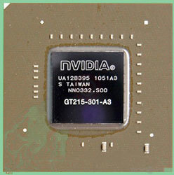
GT215-301-A3

GT215-450-A2

N11P-GV2-A3
TPC Diagram
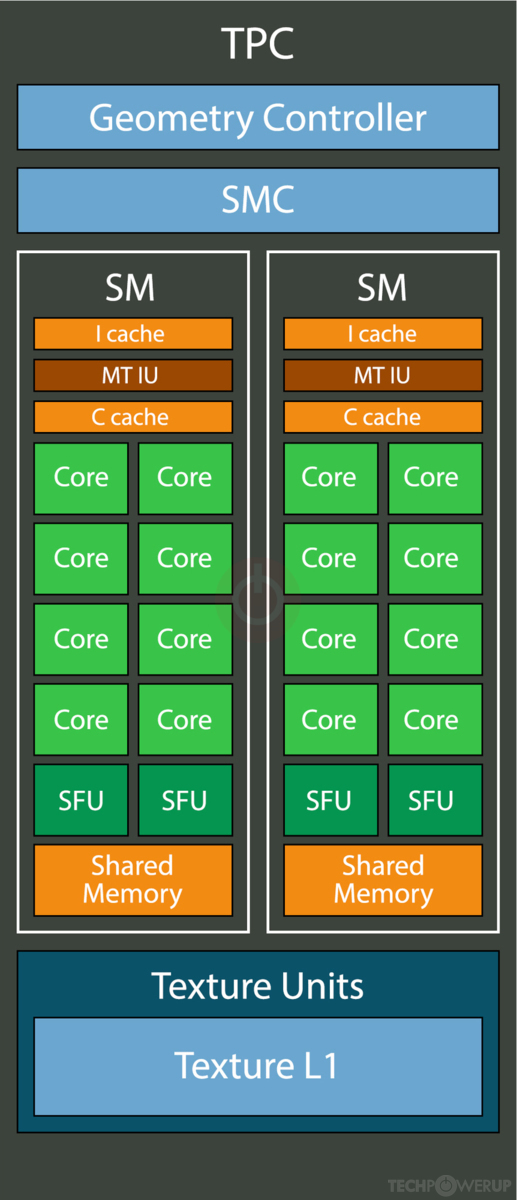
NVIDIA's GT215 GPU uses the Tesla 2.0 architecture and is made using a 40 nm production process at TSMC. With a die size of 144 mm² and a transistor count of 727 million it is a small chip. GT215 supports DirectX 11.1 (Feature Level 10_1). For GPU compute applications, OpenCL version 1.1 and CUDA 1.2 can be used. It features 96 shading units, 32 texture mapping units and 8 ROPs.
Further reading:
Tesla Architecture Whitepaper 
Graphics Processor
- Released
- Jun 15th, 2009
- GPU Name
- GT215
- Codename
- NVA3
- Architecture
- Tesla 2.0
- Foundry
- TSMC
- Process Size
- 40 nm
- Transistors
- 727 million
- Density
- 5.0M / mm²
- Die Size
- 144 mm²
- Package
- BGA-969
Graphics Features
- DirectX
- 11.1 (10_1)
- OpenGL
- 3.3
- OpenCL
- 1.1
- Vulkan
- N/A
- CUDA
- 1.2
- Shader Model
- 4.1
- WDDM
- 1.2
- PureVideo HD
- VP4
- VDPAU
- Feature Set C
Render Config
- Shading Units
- 96
- TMUs
- 32
- ROPs
- 8
- SM Count
- 12
- SFUs
- 24
- TPCs
- 6
- Tex L1 Cache
- 16 KB per TPC
- L2 Cache
- 64 KB
- Max. TDP
- 75 W
All Tesla 2.0 GPUs
NVIDIA GPU Architecture History
- 2024 Blackwell
- 2023 Hopper
- 2022-2024 Ada Lovelace
- 2020-2024 Ampere
- 2018-2022 Turing
- 2017-2020 Volta
- 2016-2021 Pascal
- 2014-2019 Maxwell 2.0
- 2014-2017 Maxwell
- 2013-2015 Kepler 2.0
- 2012-2018 Kepler
- 2010-2016 Fermi 2.0
- 2010-2013 VLIW Vec4
- 2010-2016 Fermi
- 2007-2013 Tesla 2.0
- 2006-2010 Tesla
- 2003-2013 Curie
- 2003-2005 Rankine
- 2001-2003 Kelvin
- 1999-2005 Celsius
- 1998-2000 Fahrenheit
Graphics cards using the NVIDIA GT215 GPU
| Name | Chip | Memory | Shaders | TMUs | ROPs | GPU Clock | Memory Clock |
|---|---|---|---|---|---|---|---|
| GT215-301-A3 | 1024 MB | 96 | 32 | 8 | 550 MHz | 850 MHz | |
| GT215-250-A2 | 1024 MB | 72 | 24 | 8 | 540 MHz | 790 MHz | |
| GT215-450-A2 | 1024 MB | 96 | 32 | 8 | 550 MHz | 850 MHz | |
| N11E-GS1-A3 | 1024 MB | 96 | 32 | 8 | 550 MHz | 900 MHz | |
| N10E-GS | 512 MB | 96 | 32 | 8 | 550 MHz | 850 MHz | |
| N11E-GE1 | 1024 MB | 96 | 32 | 8 | 450 MHz | 790 MHz | |
| N10P-GLM4 | 1024 MB | 72 | 24 | 8 | 560 MHz | 790 MHz | |
| N11P-GS1 | 1024 MB | 72 | 24 | 8 | 450 MHz | 790 MHz | |
| N10E-GE-A2 | 1024 MB | 96 | 32 | 8 | 450 MHz | 790 MHz | |
| GT215-301-A3 | 512 MB | 96 | 32 | 8 | 550 MHz | 1000 MHz | |
| GT215-450-A2 | 512 MB | 48 | 16 | 8 | 506 MHz | 700 MHz | |
| GT215-450-A2 | 256 MB | 48 | 16 | 4 | 506 MHz | 350 MHz | |
| GT215-301-A3 | 1024 MB | 96 | 32 | 8 | 540 MHz | 790 MHz |


GT215 GPU Notes
| PureVideo HD: VP4 VDPAU: Feature Set C |
May 21st, 2024 06:19 EDT
change timezone
Latest GPU Drivers
New Forum Posts
- 20 Years? (48)
- Would you pay more for hardware with AI capabilities? (47)
- MSI 4070 Ti Super BIOS update? (1)
- What are you playing? (20719)
- TPU's Nostalgic Hardware Club (18522)
- What's your latest tech purchase? (20606)
- SSD-Z doesn't display the core information. (1)
- Why I love Gaming (11)
- Xonotic the-big-keybench demo results (4)
- Ryzen 5 5600x stock overclocked reaching high temps (0)
Popular Reviews
- Ghost of Tsushima Performance Benchmark Review - 35 GPUs Tested
- Ghost of Tsushima: DLSS vs. FSR vs. XeSS Comparison Review
- PNY XLR8 Gaming EPIC-X RGB DDR5-6400 CL32 32 GB Review
- TerraMaster D8 Hybrid Review
- Silverstone Shark Force 120 mm Fan Review
- Homeworld 3 Performance Benchmark Review - 35 GPUs Tested
- Upcoming Hardware Launches 2023 (Updated Feb 2024)
- Lofree Edge Ultra-Low Profile Wireless Mechanical Keyboard Review
- AMD Ryzen 7 7800X3D Review - The Best Gaming CPU
- AMD Ryzen 7 7700 Review - Affordable Zen 4 Powerhouse
Controversial News Posts
- Intel Statement on Stability Issues: "Motherboard Makers to Blame" (269)
- AMD to Redesign Ray Tracing Hardware on RDNA 4 (227)
- Windows 11 Now Officially Adware as Microsoft Embeds Ads in the Start Menu (173)
- NVIDIA to Only Launch the Flagship GeForce RTX 5090 in 2024, Rest of the Series in 2025 (154)
- AMD Hits Highest-Ever x86 CPU Market Share in Q1 2024 Across Desktop and Server (140)
- AMD RDNA 5 a "Clean Sheet" Graphics Architecture, RDNA 4 Merely Corrects a Bug Over RDNA 3 (139)
- AMD's RDNA 4 GPUs Could Stick with 18 Gbps GDDR6 Memory (114)
- AMD Ryzen 9 7900X3D Now at a Mouth-watering $329 (104)