Intel Could Develop its own big.LITTLE x86 Adaptation
big.LITTLE is an innovation by ARM, which seeks to minimize power-draw on mobile devices. It is a sort of heterogeneous multi-core CPU design, in which a few "big" high-performance CPU cores work alongside a few extremely low-power "little" CPU cores. The idea here is that the low-power cores consume much lesser power at max load, than the high-performance cores at their minimum power-state, so the high-performance cores can be power-gated when the system doesn't need them (i.e. most of the time).
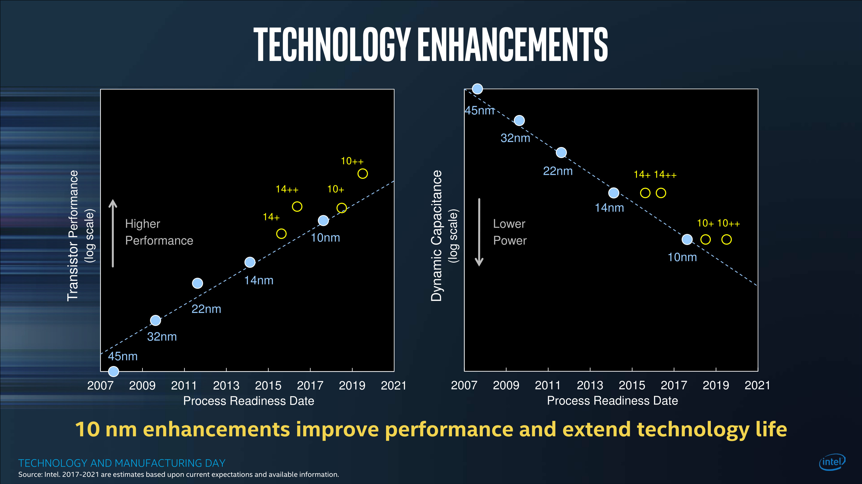
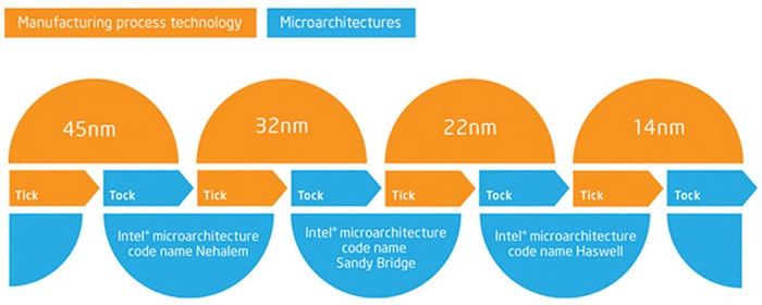
Intel finds itself with two distinct x86 implementations at any given time. It has low-power CPU micro-architectures such as "Silvermont," "Goldmont," and "Goldmont Plus," etc., implemented on low-power product lines such as the Pentium Silver series; and it has high-performance micro-architectures, such as "Haswell," "Skylake," and "Coffee Lake." The company wants to take a swing at its own heterogeneous multi-core CPU, according to tech stock analyst Ashraf Eassa, with the Motley Fool.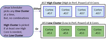
Intel finds itself with two distinct x86 implementations at any given time. It has low-power CPU micro-architectures such as "Silvermont," "Goldmont," and "Goldmont Plus," etc., implemented on low-power product lines such as the Pentium Silver series; and it has high-performance micro-architectures, such as "Haswell," "Skylake," and "Coffee Lake." The company wants to take a swing at its own heterogeneous multi-core CPU, according to tech stock analyst Ashraf Eassa, with the Motley Fool.